

NSC LM3405XMKX, LM3405 Datasheet
February 2007
LM3405
1.6MHz, 1A Constant Current Buck Regulator for Powering
LEDs
General Description
Integrated with a 1A power switch, the LM3405 is a currentmode control switching buck regulator designed to provide a
simple, high efficiency solution for driving high power LEDs.
With a 0.205V reference voltage feedback control to minimize
power dissipation, an external resistor sets the current as
needed for driving various types of LEDs. Switching frequency is internally set to 1.6MHz, allowing small surface mount
inductors and capacitors to be used. The LM3405 utilizes
current-mode control and internal compensation offering
ease of use and predictable, high performance regulation
over a wide range of operating conditions. Additional features
include user accessible EN/DIM pin for enabling and PWM
dimming of LEDs, thermal shutdown, cycle-by-cycle current
limit and over-current protection.
Features
■
VIN operating range of 3V to 15V
■
Thin SOT23-6 package
■
1.6MHz switching frequency
■
300mΩ NMOS switch
■
40nA shutdown current at VIN = 5V
■
EN/DIM input for enabling and PWM dimming of LEDs
■
Internally compensated current-mode control
■
Cycle-by-cycle current limit
■
Input voltage UVLO
■
Over-current protection
■
Thermal shutdown
Applications
■
LED Driver
■
Constant Current Source
■
Industrial Lighting
■
LED Flashlights
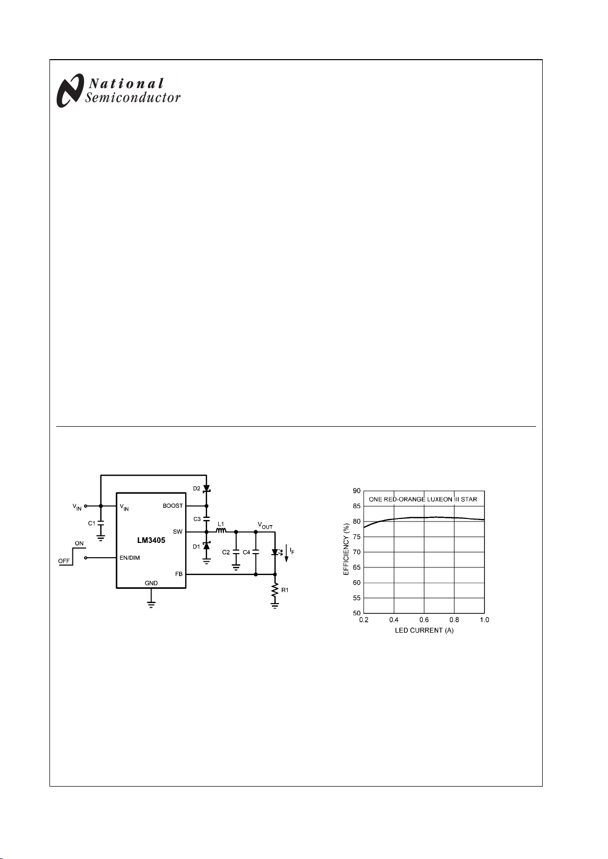
Typical Application Circuit
20178901
Efficiency vs LED Current (V
IN
= 5V)
20178971
© 2007 National Semiconductor Corporation 201789 www.national.com
LM3405 1.6MHz, 1A Constant Current Buck Regulator for Powering LEDs
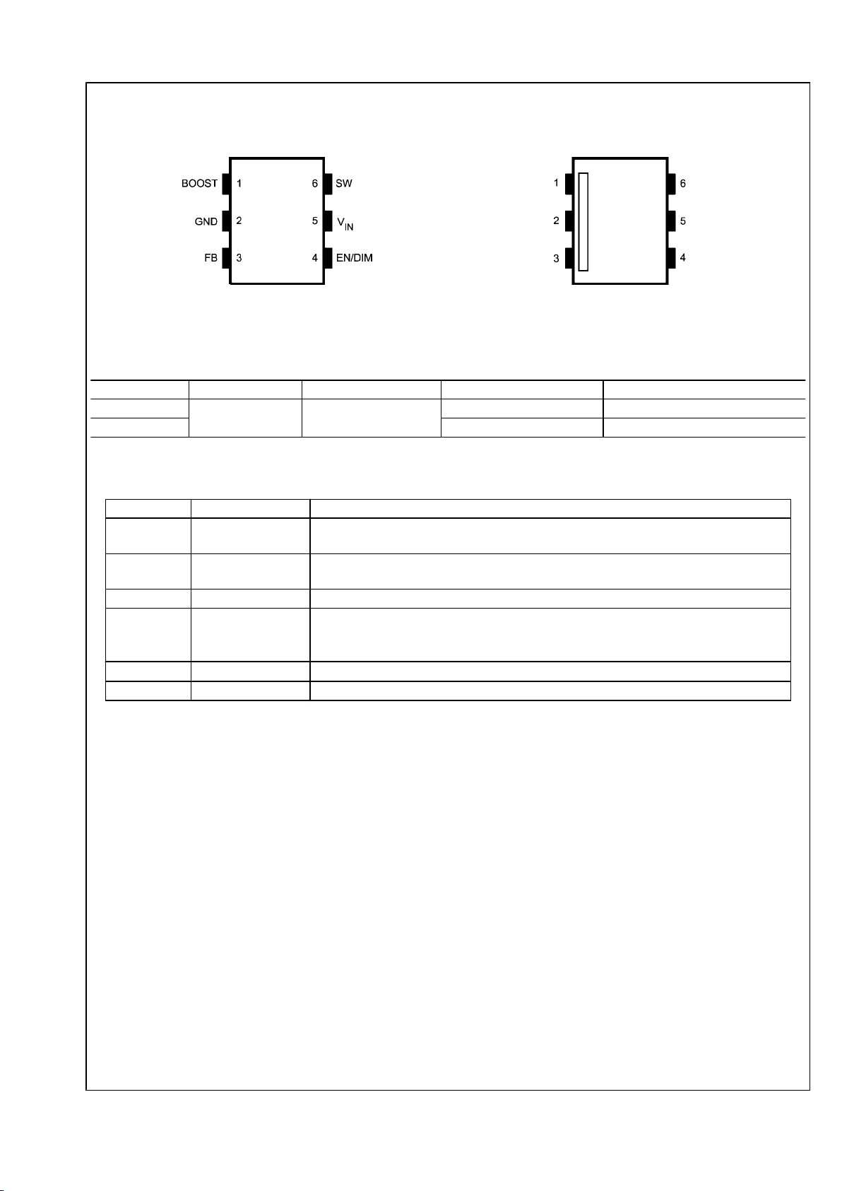
Connection Diagrams
20178905
6-Lead TSOT
NS Package Number MK06A
20178960
Pin 1 Identification
Ordering Information
Part Number Package Type NS Package Drawing Package Marking Supplied As
LM3405XMK
TSOT-6 MK06A
SPNB 1000 Units on Tape and Reel
LM3405XMKX SPNB 3000 Units on Tape and Reel
*NOPB versions are available
Pin Descriptions
Pin(s) Name Application Information
1 BOOST
Voltage at this pin drives the internal NMOS power switch. A bootstrap capacitor is
connected between the BOOST and SW pins.
2 GND
Signal and Power ground pin. Place the LED current-setting resistor as close as possible
to this pin for accurate current regulation.
3 FB Feedback pin. Connect an external resistor from FB to GND to set the LED Current.
4 EN/DIM
Enable control input. Logic high enables operation. Toggling this pin with a periodic logic
square wave of varying duty cycle at different frequencies controls the brightness of LEDs.
Do not allow this pin to float or be greater than VIN + 0.3V.
5 V
IN
Input supply voltage. Connect a bypass capacitor locally from this pin to GND.
6 SW Switch pin. Connect this pin to the inductor, catch diode, and bootstrap capacitor.
www.national.com 2
LM3405
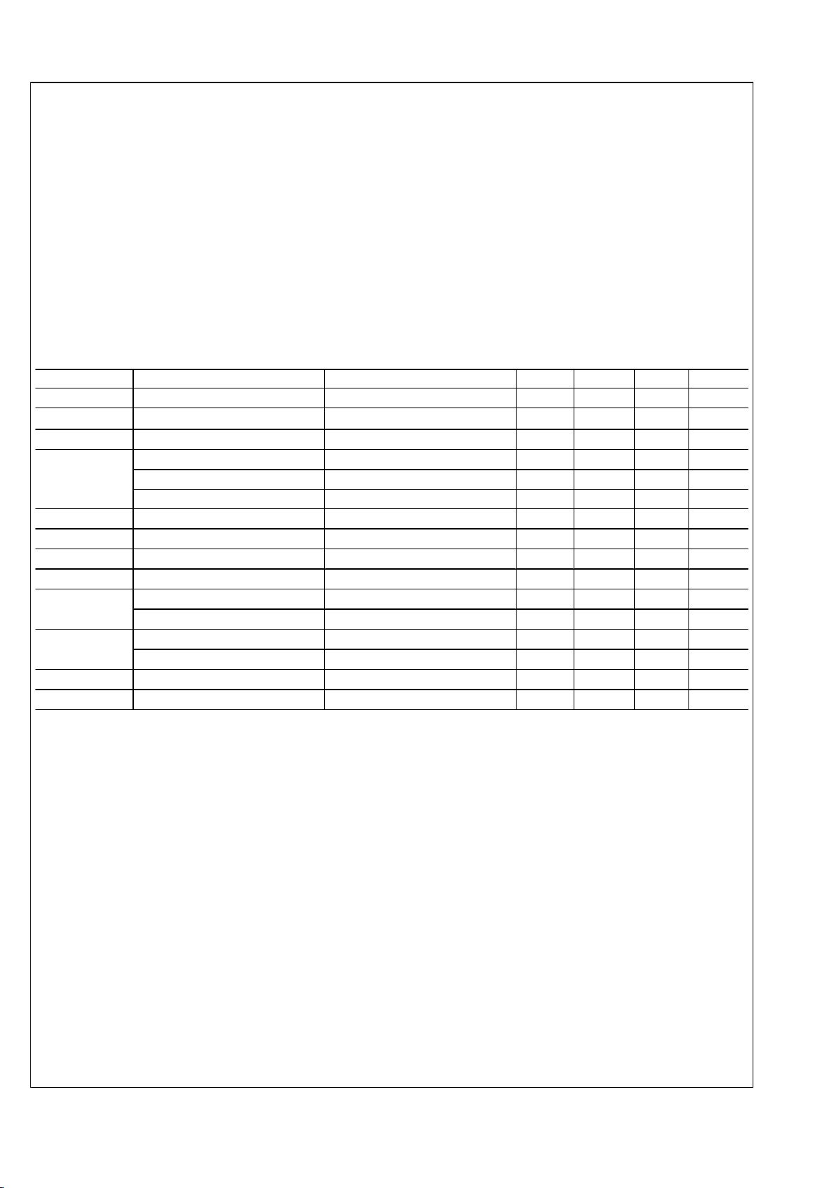
Absolute Maximum Ratings (Note 1)
If Military/Aerospace specified devices are required,
please contact the National Semiconductor Sales Office/
Distributors for availability and specifications.
V
IN
-0.5V to 20V
SW Voltage -0.5V to 20V
Boost Voltage -0.5V to 26V
Boost to SW Voltage -0.5V to 6.0V
FB Voltage -0.5V to 3.0V
EN/DIM Voltage
-0.5V to (VIN + 0.3V)
Junction Temperature 150°C
ESD Susceptibility (Note 2) 2kV
Storage Temperature -65°C to +150°C
Soldering Information
Infrared/Convection Reflow (15sec) 220°C
Operating Ratings (Note 1)
V
IN
3V to 15V
EN/DIM voltage
-0.5V to (VIN + 0.3V)
Boost to SW Voltage 2.5V to 5.5V
Junction Temperature Range -40°C to +125°C
Thermal Resistance θJA (Note 3)
118°C/W
Electrical Characteristics Unless otherwise specified, V
IN
= 12V. Limits in standard type are for TJ = 25°C only;
limits in boldface type apply over the junction temperature (TJ) range of -40°C to +125°C. Minimum and Maximum limits are
guaranteed through test, design, or statistical correlation. Typical values represent the most likely parametric norm, and are
provided for reference purposes only.
Symbol Parameter Conditions Min Typ Max Units
V
FB
Feedback Voltage 0.188 0.205 0.220 V
ΔVFB/(ΔVINxVFB)
Feedback Voltage Line Regulation
VIN = 3V to 15V
0.01
%/V
I
FB
Feedback Input Bias Current
Sink/Source 10 250
nA
UVLO
Under-voltage Lockout
VIN Rising 2.74 2.95
V
Under-voltage Lockout VIN Falling 1.9 2.3 V
UVLO Hysteresis 0.44 V
f
SW
Switching Frequency 1.2 1.6 1.9 MHz
D
MAX
Maximum Duty Cycle VFB = 0V 85 94 %
R
DS(ON)
Switch ON Resistance V
BOOST
- VSW = 3V 300 600
mΩ
I
CL
Switch Current Limit V
BOOST
- VSW = 3V, VIN = 3V 1.2 2.0 2.8 A
I
Q
Quiescent Current Switching, VFB = 0.195V 1.8 2.8 mA
Quiescent Current (Shutdown) V
EN/DIM
= 0V 0.3 µA
V
EN/DIM_TH
Enable Threshold Voltage
V
EN/DIM
Rising 1.8
V
Shutdown Threshold Voltage
V
EN/DIM
Falling 0.4
V
I
EN/DIM
EN/DIM Pin Current Sink/Source 0.01 µA
I
SW
Switch Leakage VIN = 15V 0.1
µA
Note 1: Absolute Maximum Ratings are limits beyond which damage to the device may occur. Operating Ratings define the conditions under which the device
is intended to be functional. For guaranteed specifications and test conditions, see the Electrical Characteristics.
Note 2: Human body model, 1.5kΩ in series with 100pF.
Note 3: Thermal shutdown will occur if the junction temperature (TJ) exceeds 165°C. The maximum allowable power dissipation (PD) at any ambient temperature
(TA) is PD = (T
J(MAX)
– TA)/θJA . This number applies to packages soldered directly onto a 3" x 3" PC board with 2oz. copper on 4 layers in still air. For a 2 layer
board using 1 oz. copper in still air, θJA = 204°C/W.
3 www.national.com
LM3405
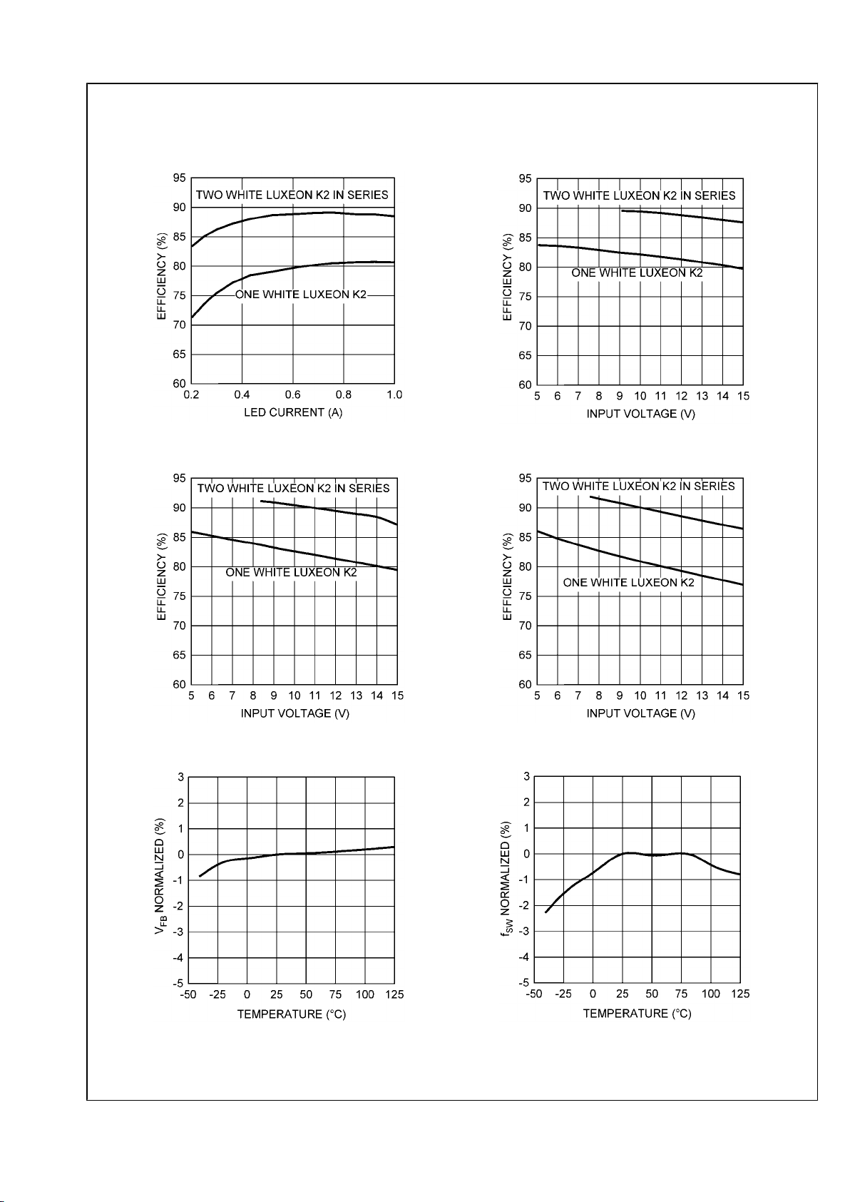
Typical Performance Characteristics Unless otherwise specified, V
IN
= 12V, V
BOOST
- VSW = 5V and
TA = 25°C.
Efficiency vs LED Current
20178973
Efficiency vs Input Voltage (IF = 1A)
20178931
Efficiency vs Input Voltage (IF = 0.7A)
20178932
Efficiency vs Input Voltage (IF = 0.35A)
20178933
VFB vs Temperature
20178927
Oscillator Frequency vs Temperature
20178936
www.national.com 4
LM3405
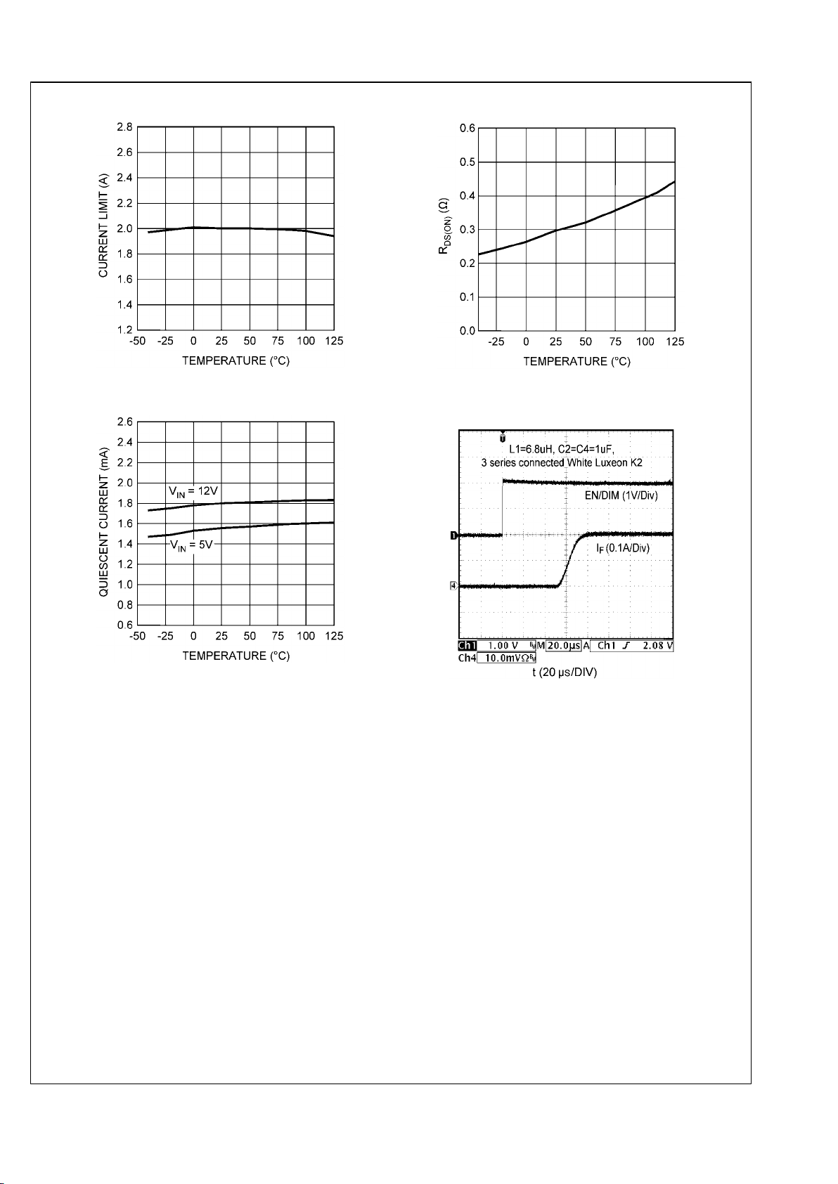
Current Limit vs Temperature
20178972
R
DS(ON)
vs Temperature (V
BOOST
- VSW = 3V)
20178930
Quiescent Current vs Temperature
20178934
Startup Response to EN/DIM Signal
(VIN = 15V, IF = 0.2A)
20178968
5 www.national.com
LM3405
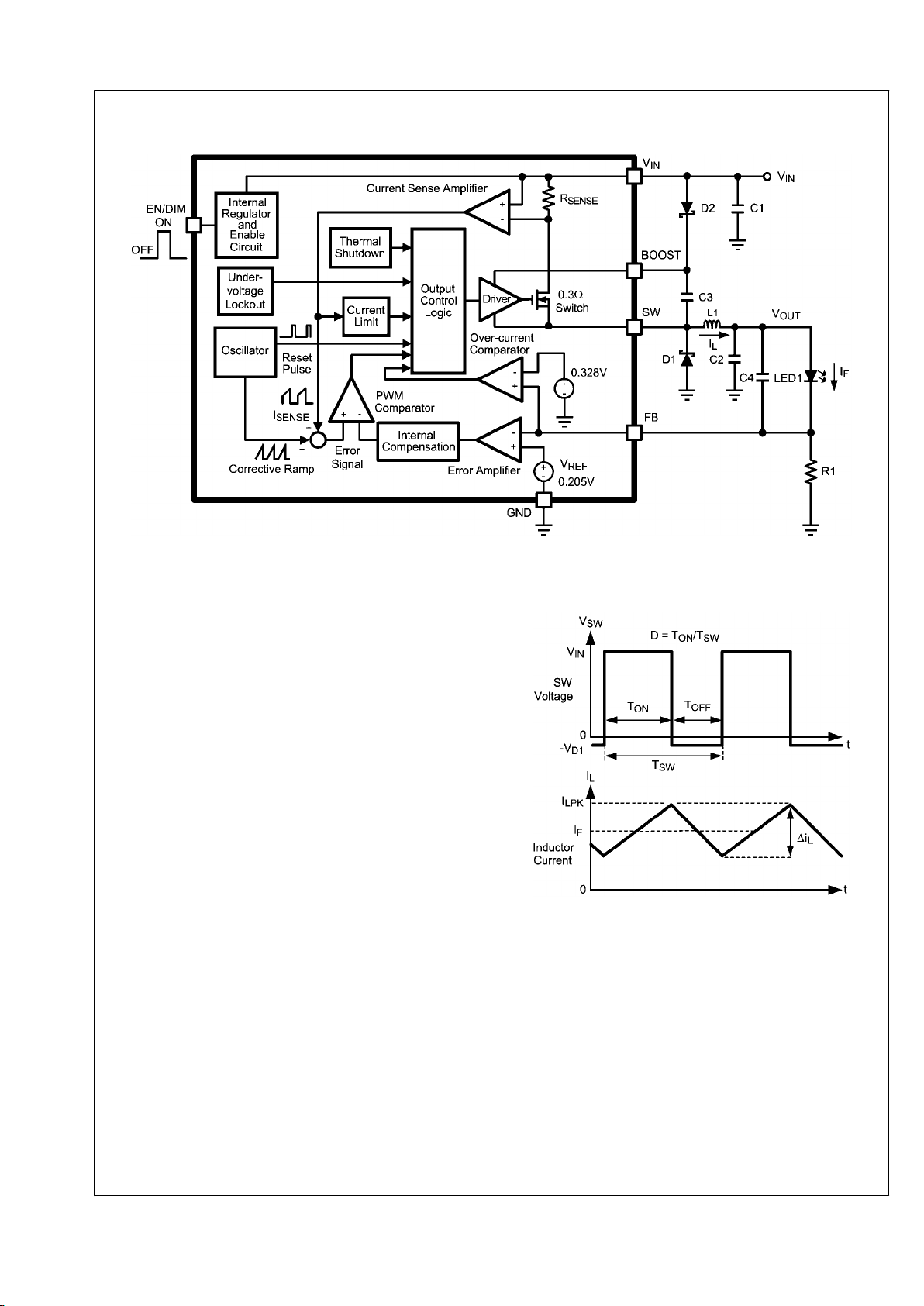
Block Diagram
20178906
FIGURE 1. Simplified Block Diagram
Application Information
THEORY OF OPERATION
The LM3405 is a PWM, current-mode control switching buck
regulator designed to provide a simple, high efficiency solution for driving LEDs with a preset switching frequency of
1.6MHz. This high frequency allows the LM3405 to operate
with small surface mount capacitors and inductors, resulting
in LED drivers that need only a minimum amount of board
space. The LM3405 is internally compensated, simple to use,
and requires few external components.
The following description of operation of the LM3405 will refer
to the Simplified Block Diagram (Figure 1) and to the waveforms in Figure 2. The LM3405 supplies a regulated output
current by switching the internal NMOS power switch at constant frequency and variable duty cycle. A switching cycle
begins at the falling edge of the reset pulse generated by the
internal oscillator. When this pulse goes low, the output control logic turns on the internal NMOS power switch. During this
on-time, the SW pin voltage (VSW) swings up to approximately
VIN, and the inductor current (IL) increases with a linear slope.
IL is measured by the current sense amplifier, which generates an output proportional to the switch current. The sense
signal is summed with the regulator’s corrective ramp and
compared to the error amplifier’s output, which is proportional
to the difference between the feedback voltage and V
REF
.
When the PWM comparator output goes high, the internal
power switch turns off until the next switching cycle begins.
During the switch off-time, inductor current discharges
through the catch diode D1, which forces the SW pin to swing
below ground by the forward voltage (VD1) of the catch diode.
The regulator loop adjusts the duty cycle (D) to maintain a
constant output current (IF) through the LED, by forcing FB
pin voltage to be equal to V
REF
(0.205V).
20178907
FIGURE 2. SW Pin Voltage and Inductor Current
Waveforms of LM3405
BOOST FUNCTION
Capacitor C3 and diode D2 in Figure 1 are used to generate
a voltage V
BOOST
. The voltage across C3, V
BOOST
- VSW, is
the gate drive voltage to the internal NMOS power switch. To
properly drive the internal NMOS switch during its on-time,
V
BOOST
needs to be at least 2.5V greater than VSW. Large
value of V
BOOST
- VSW is recommended to achieve better efficiency by minimizing both the internal switch ON resistance
(R
DS(ON)
), and the switch rise and fall times. However,
V
BOOST
- VSW should not exceed the maximum operating limit
of 5.5V.
www.national.com 6
LM3405
 Loading...