

NSC LM3404, LM3404MRX Datasheet
June 2007
LM3404/04HV
1.0A Constant Current Buck Regulator for Driving High
Power LEDs
General Description
The LM3404/04HV are monolithic switching regulators designed to deliver constant currents to high power LEDs. Ideal
for automotive, industrial, and general lighting applications,
they contain a high-side N-channel MOSFET switch with a
current limit of 1.5A (typical) for step-down (Buck) regulators.
Hysteretic controlled on-time and an external resistor allow
the converter output voltage to adjust as needed to deliver a
constant current to series and series-parallel connected LED
arrays of varying number and type. LED dimming via pulse
width modulation (PWM), broken/open LED protection, lowpower shutdown and thermal shutdown complete the feature
set.
Features
■
Integrated 1.0A MOSFET
■
VIN Range 6V to 42V (LM3404)
■
VIN Range 6V to 75V (LM3404HV)
■
1.2A Output Current Over Temperature
■
Cycle-by-Cycle Current Limit
■
No Control Loop Compensation Required
■
Separate PWM Dimming and Low Power Shutdown
■
Supports all-ceramic output capacitors and capacitor-less
outputs
■
Thermal shutdown protection
■
SO-8 Package, PSOP-8 Package
Applications
■
LED Driver
■
Constant Current Source
■
Automotive Lighting
■
General Illumination
■
Industrial Lighting
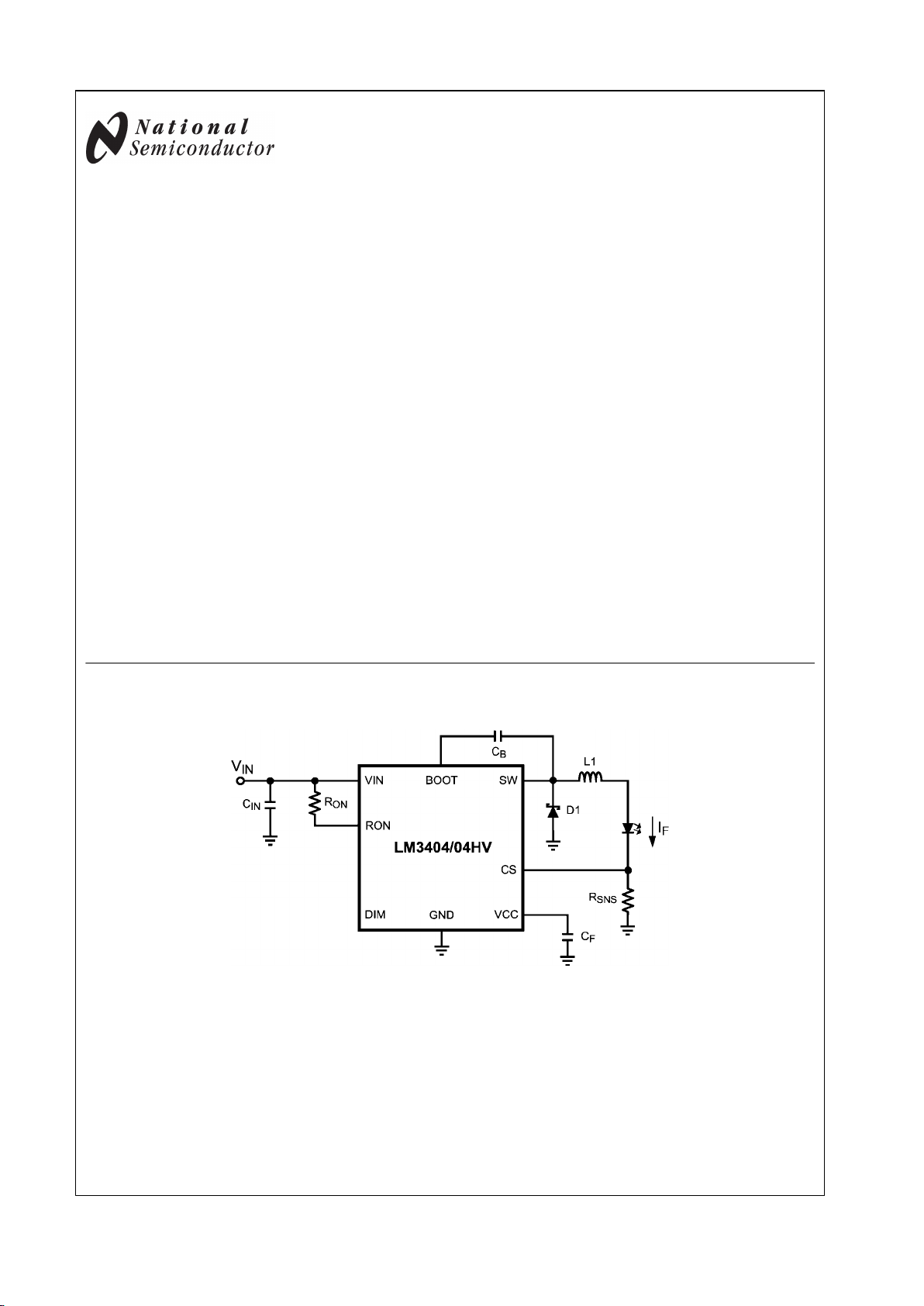
Typical Application
20205401
© 2007 National Semiconductor Corporation 202054 www.national.com
LM3404/04HV 1.0A Constant Current Buck Regulator for Driving High Power LEDs
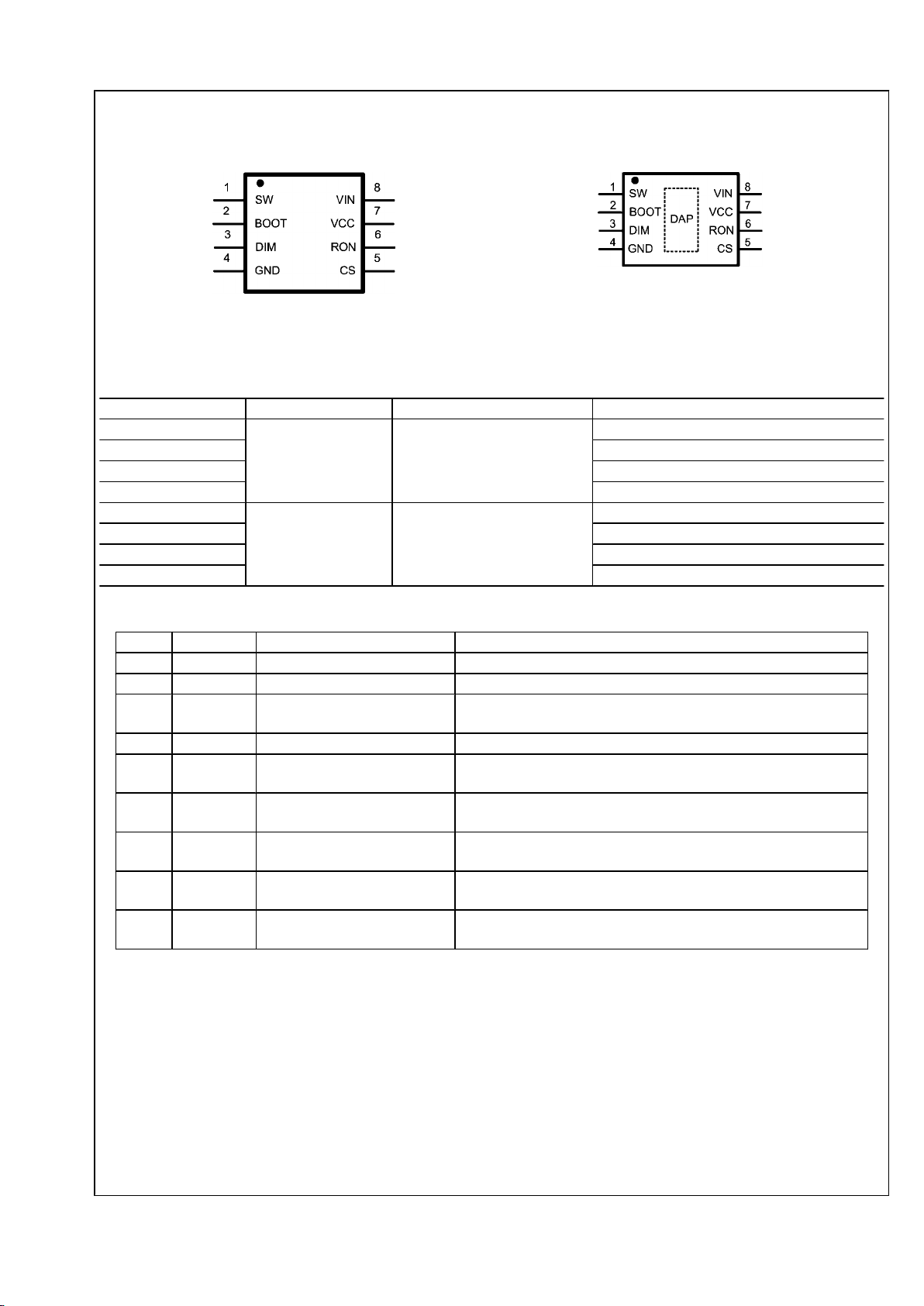
Connection Diagrams
20205402
8-Lead Plastic SO-8 Package
NS Package Number M08A
20205456
8-Lead Plastic PSOP-8 Package
NS Package Number MRA08B
Ordering Information
Order Number Package Type NSC Package Drawing Supplied As
LM3404MA
SO-8 M08A
95 units in anti-static rails
LM3404MAX 2500 units on tape and reel
LM3404HVMA 95 units in anti-static rails
LM3404HVMAX 2500 units on tape and reel
LM3404MR
PSOP-8 MRA08B
95 units in anti-static rails
LM3404MRX 2500 units on tape and reel
LM3404HVMR 95 units in anti-static rails
LM3404HVMRX 2500 units on tape and reel
Pin Descriptions
Pin(s) Name Description Application Information
1 SW Switch pin Connect this pin to the output inductor and Schottky diode.
2 BOOT MOSFET drive bootstrap pin Connect a 10 nF ceramic capacitor from this pin to SW.
3 DIM Input for PWM dimming Connect a logic-level PWM signal to this pin to enable/disable the
power MOSFET and reduce the average light output of the LED array.
4 GND Ground pin Connect this pin to system ground.
5 CS Current sense feedback pin Set the current through the LED array by connecting a resistor from
this pin to ground.
6 RON On-time control pin A resistor connected from this pin to VIN sets the regulator controlled
on-time.
7 VCC Output of the internal 7V linear
regulator
Bypass this pin to ground with a minimum 0.1 µF ceramic capacitor
with X5R or X7R dielectric.
8 VIN Input voltage pin Nominal operating input range for this pin is 6V to 42V (LM3404) or 6V
to 75V (LM3404HV).
DAP GND Thermal Pad Connect to ground. Place 4-6 vias from DAP to bottom layer ground
plane.
www.national.com 2
LM3404/LM3404HV

Absolute Maximum Ratings
(LM3404) (Note 1)
If Military/Aerospace specified devices are required,
please contact the National Semiconductor Sales Office/
Distributors for availability and specifications.
VIN to GND -0.3V to 45V
BOOT to GND -0.3V to 59V
SW to GND -1.5V to 45V
BOOT to VCC -0.3V to 45V
BOOT to SW -0.3V to 14V
VCC to GND -0.3V to 14V
DIM to GND -0.3V to 7V
CS to GND -0.3V to 7V
RON to GND -0.3V to 7V
Junction Temperature 150°C
Storage Temp. Range -65°C to 125°C
ESD Rating (Note 2) 2kV
Soldering Information
Lead Temperature (Soldering,
10sec) 260°C
Infrared/Convection Reflow (15sec) 235°C
Operating Ratings (LM3404)
(Note 1)
V
IN
6V to 42V
Junction Temperature Range −40°C to +125°C
Thermal Resistance θ
JA
(SO-8 Package) 155°C/W
Thermal Resistance θ
JA
(PSOP-8 Package) (Note 5) 50°C/W
3 www.national.com
LM3404/LM3404HV

Absolute Maximum Ratings
(LM3404HV) (Note 1)
If Military/Aerospace specified devices are required,
please contact the National Semiconductor Sales Office/
Distributors for availability and specifications.
VIN to GND
-0.3V to 76V
BOOT to GND -0.3V to 90V
SW to GND -1.5V to 76V
BOOT to VCC -0.3V to 76V
BOOT to SW -0.3V to 14V
VCC to GND -0.3V to 14V
DIM to GND -0.3V to 7V
CS to GND -0.3V to 7V
RON to GND -0.3V to 7V
Junction Temperature 150°C
Storage Temp. Range -65°C to 125°C
ESD Rating (Note 2) 2kV
Soldering Information
Lead Temperature (Soldering,
10sec) 260°C
Infrared/Convection Reflow (15sec) 235°C
Operating Ratings (LM3404HV)
(Note 1)
V
IN
6V to 75V
Junction Temperature Range −40°C to +125°C
Thermal Resistance θ
JA
(SO-8 Package) 155°C/W
Thermal Resistance θ
JA
(PSOP-8 Package) (Note 5) 50°C/W
www.national.com 4
LM3404/LM3404HV
Electrical Characteristics V
IN
= 24V unless otherwise indicated. Typicals and limits appearing in plain type apply
for TA = TJ = +25°C. (Note 4) Limits appearing in boldface type apply over full Operating Temperature Range. Datasheet min/
max specification limits are guaranteed by design, test, or statistical analysis.
LM3404
Symbol Parameter Conditions Min Typ Max Units
SYSTEM PARAMETERS
t
ON-1
On-time 1
VIN = 10V, RON = 200 kΩ
2.1 2.75 3.4 µs
t
ON-2
On-time 2
VIN = 40V, RON = 200 kΩ
515 675 835 ns
LM3404HV
Symbol Parameter Conditions Min Typ Max Units
SYSTEM PARAMETERS
t
ON-1
On-time 1
VIN = 10V, RON = 200 kΩ
2.1 2.75 3.4 µs
t
ON-2
On-time 2
VIN = 70V, RON = 200 kΩ
325 415 505 ns
LM3404/LM3404HV
Symbol Parameter Conditions Min Typ Max Units
REGULATION AND OVER-VOLTAGE COMPARATORS
V
REF-REG
CS Regulation Threshold CS Decreasing, SW turns on 194 200 206 mV
V
REF-0V
CS Over-voltage Threshold CS Increasing, SW turns off 300 mV
I
CS
CS Bias Current CS = 0V 0.1 µA
SHUTDOWN
V
SD-TH
Shutdown Threshold RON / SD Increasing 0.3 0.7 1.05 V
V
SD-HYS
Shutdown Hysteresis RON / SD Decreasing 40 mV
OFF TIMER
t
OFF-MIN
Minimum Off-time CS = 0V 270 ns
INTERNAL REGULATOR
V
CC-REG
VCC Regulated Output 6.4 7 7.4 V
V
IN-DO
VIN - V
CC
ICC = 5 mA, 6.0V < VIN < 8.0V 300 mV
V
CC-BP-TH
VCC Bypass Threshold VIN Increasing 8.8 V
V
CC-BP-HYS
VCC Bypass Hysteresis VIN Decreasing 230 mV
V
CC-Z-6
VCC Output Impedance
(0 mA < ICC < 5 mA)
VIN = 6V 55
Ω
V
CC-Z-8
VIN = 8V 50
V
CC-Z-24
VIN = 24V 0.4
V
CC-LIM
VCC Current Limit (Note 3) VIN = 24V, VCC = 0V 16 mA
V
CC-UV-TH
VCC Under-voltage Lock-out
Threshold
VCC Increasing 5.3 V
V
CC-UV-HYS
VCC Under-voltage Lock-out
Hysteresis
VCC Decreasing 150 mV
V
CC-UV-DLY
VCC Under-voltage Lock-out
Filter Delay
100 mV Overdrive 3 µs
I
IN-OP
I
IN
Operating Current Non-switching, CS = 0.5V 625 900 µA
I
IN-SD
IIN Shutdown Current RON / SD = 0V 95 180 µA
CURRENT LIMIT
I
LIM
Current Limit Threshold 1.2 1.5 1.8 A
5 www.national.com
LM3404/LM3404HV
Symbol Parameter Conditions Min Typ Max Units
DIM COMPARATOR
V
IH
Logic High DIM Increasing 2.2 V
V
IL
Logic Low DIM Decreasing 0.8 V
I
DIM-PU
DIM Pull-up Current DIM = 1.5V 80 µA
MOSFET AND DRIVER
R
DS-ON
Buck Switch On Resistance ISW = 200mA, BST-SW = 6.3V 0.37 0.75
Ω
V
DR-UVLO
BST Under-voltage Lock-out
Threshold
BST–SW Increasing 1.7 3 4 V
V
DR-HYS
BST Under-voltage Lock-out
Hysteresis
BST–SW Decreasing 400 mV
THERMAL SHUTDOWN
T
SD
Thermal Shutdown Threshold 165 °C
T
SD-HYS
Thermal Shutdown Hysteresis 25 °C
THERMAL RESISTANCE
θ
JA
Junction to Ambient SOIC-8 Package 155 °C/W
PSOP-8 Package (Note 5) 50
Note 1: Absolute Maximum Ratings indicate limits beyond which damage to the device may occur. Operating Ratings indicate conditions for which the device is
intended to be functional, but specific performance is not guaranteed. For guaranteed specifications and the test conditions, see Electrical Characteristics.
Note 2: The human body model is a 100 pF capacitor discharged through a 1.5 kΩ resistor into each pin.
Note 3: VCC provides self bias for the internal gate drive and control circuits. Device thermal limitations limit external loading.
Note 4: Typical specifications represent the most likely parametric norm at 25°C operation.
Note 5: θJA of 50°C/W with DAP soldered to a minimum of 2 square inches of 1oz. copper on the top or bottom PCB layer.
www.national.com 6
LM3404/LM3404HV
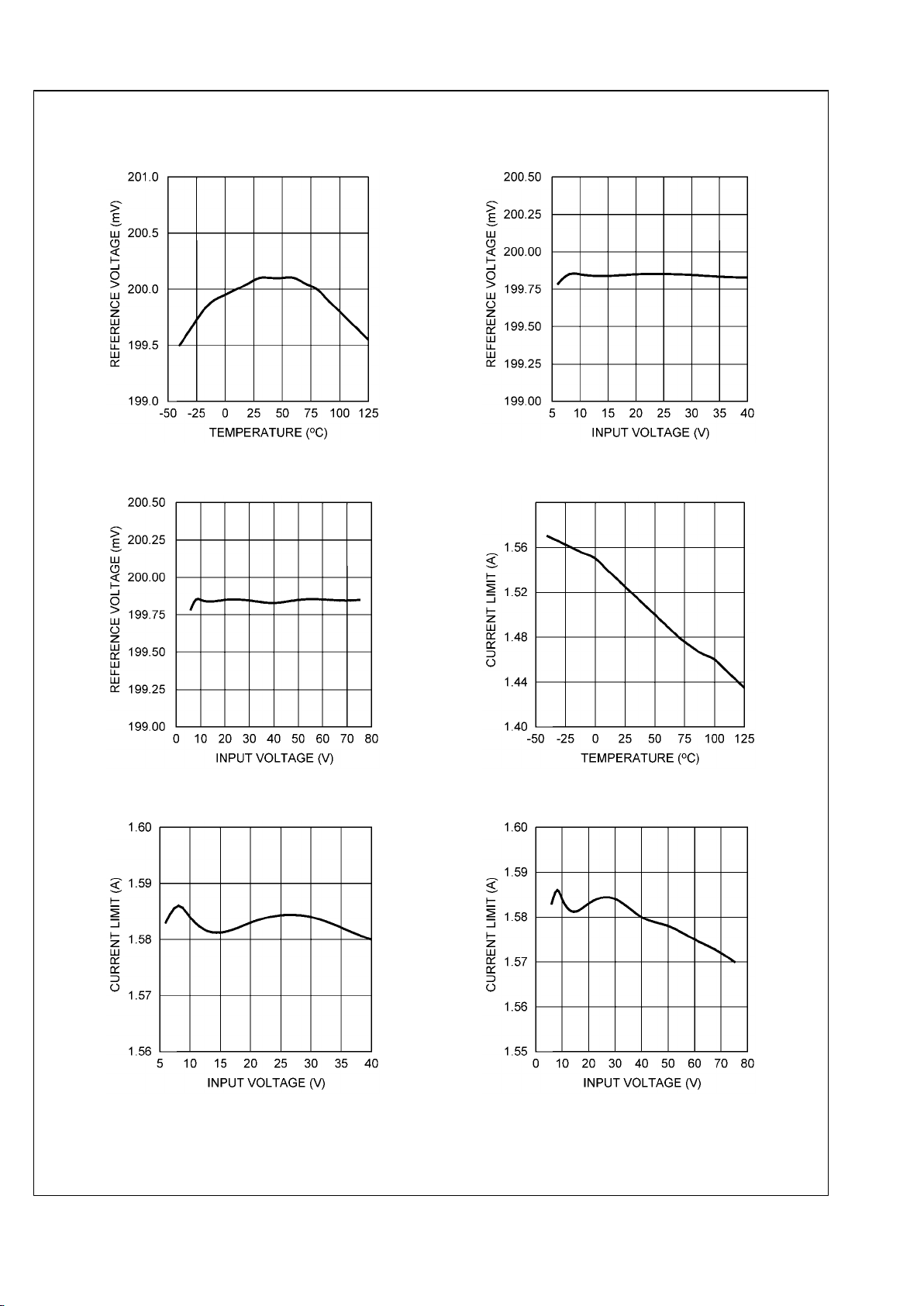
Typical Performance Characteristics
V
REF
vs Temperature (VIN = 24V)
20205450
V
REF
vs VIN, LM3404 (TA = 25°C)
20205451
V
REF
vs VIN, LM3404HV (TA = 25°C)
20205452
Current Limit vs Temperature (VIN = 24V)
20205453
Current Limit vs VIN, LM3404 (TA = 25°C)
20205454
Current Limit vs VIN, LM3404HV (TA = 25°C)
20205455
7 www.national.com
LM3404/LM3404HV
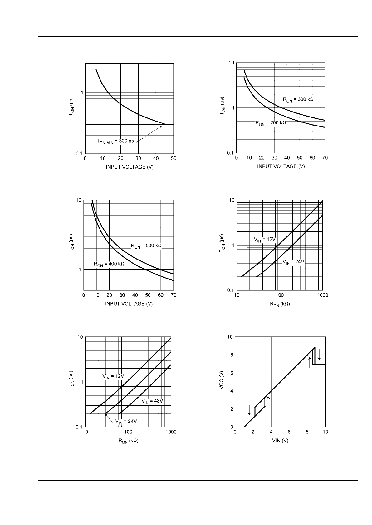
TON vs VIN,
RON = 100 kΩ (TA = 25°C)
20205435
TON vs VIN,
(TA = 25°C)
20205436
TON vs VIN,
(TA = 25°C)
20205437
TON vs RON, LM3404
(TA = 25°C)
20205444
TON vs RON, LM3404HV
(TA = 25°C)
20205438
VCC vs V
IN
(TA = 25°C)
20205439
www.national.com 8
LM3404/LM3404HV
 Loading...