

NSC LM339J, LM239AJ Datasheet
LM139/LM239/LM339/LM2901/LM3302
Low Power Low Offset Voltage Quad Comparators
LM139/LM239/LM339/LM2901/LM3302 Low Power Low Offset Voltage Quad Comparators
August 2000
General Description
The LM139 series consists of four independent precision
voltage comparators with an offset voltage specification as
low as 2 mV max for all four comparators. These were
designed specifically to operate from a single power supply
over a wide range of voltages. Operation from split power
supplies is also possible and the low power supply current
drain is independent of the magnitude of the power supply
voltage. These comparators also have a unique
characteristic in that the input common-mode voltage range
includes ground, even though operated from a single power
supply voltage.
Application areas include limitcomparators,simpleanalogto
digital converters; pulse, squarewave and time delay
generators; wide range VCO; MOS clock timers;
multivibrators and high voltage digital logic gates. The
LM139 series was designed to directly interface with TTL
and CMOS. When operated from both plus and minus power
supplies, they will directly interface with MOS logic— where
the low power drain of the LM339 is a distinct advantage
over standard comparators.
Features
n Wide supply voltage range
n LM139/139A Series 2 to 36 V
n LM2901: 2 to 36 V
n LM3302: 2 to 28 V
n Very low supply current drain (0.8 mA) — independent
of supply voltage
n Low input biasing current: 25 nA
n Low input offset current:
n Offset voltage:
n Input common-mode voltage range includes GND
n Differential input voltage range equal to the power
supply voltage
n Low output saturation voltage: 250 mV at 4 mA
n Output voltage compatible with TTL, DTL, ECL, MOS
and CMOS logic systems
DC
DC
or±1to±18 V
DC
or±1to±18 V
or±1to±14 V
±
5nA
±
3mV
DC
DC
DC
Advantages
n High precision comparators
n Reduced V
n Eliminates need for dual supplies
n Allows sensing near GND
n Compatible with all forms of logic
n Power drain suitable for battery operation
drift over temperature
OS
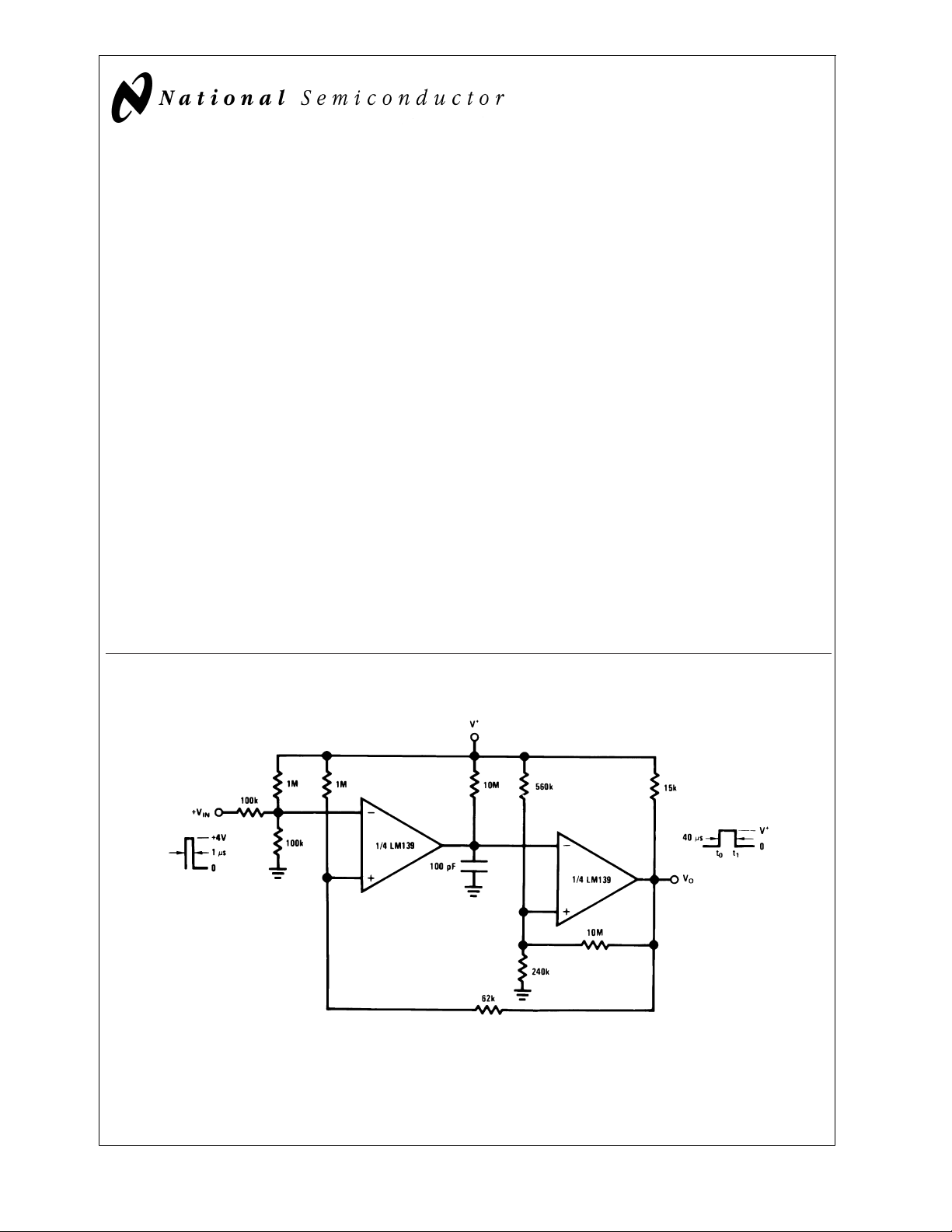
One-Shot Multivibrator with Input Lock Out
DS005706-12
© 2001 National Semiconductor Corporation DS005706 www.national.com
Absolute Maximum Ratings (Note 10)
If Military/Aerospace specified devices are required, please contact the National Semiconductor Sales
Office/Distributors for availability and specifications.
LM139/LM239/LM339
LM139A/LM239A/LM339A LM3302
Supply Voltage, V
+
Differential Input Voltage (Note 8) 36 V
Input Voltage −0.3 VDCto +36 V
Input Current (V
<
−0.3 VDC),
IN
(Note 3) 50 mA 50 mA
Power Dissipation (Note 1)
Molded DIP 1050 mW 1050 mW
LM139/LM239/LM339/LM2901/LM3302
Cavity DIP 1190 mW
Small Outline Package 760 mW
Output Short-Circuit to GND,
(Note 2) Continuous Continuous
Storage Temperature Range −65˚C to +150˚C −65˚C to +150˚C
Lead Temperature
(Soldering, 10 seconds) 260˚C 260˚C
Operating Temperature Range −40˚C to +85˚C
LM339/LM339A 0˚C to +70˚C
LM239/LM239A −25˚C to +85˚C
LM2901 −40˚C to +85˚C
LM139/LM139A −55˚C to +125˚C
Soldering Information
Dual-In-Line Package
Soldering (10 seconds) 260˚C 260˚C
Small Outline Package
Vapor Phase (60 seconds) 215˚C 215˚C
Infrared (15 seconds) 220˚C 220˚C
See AN-450 “Surface Mounting Methods and Their Effect on Product Reliability” for other methods of soldering surface mount
devices.
ESD rating (1.5 kΩ in series with 100 pF) 600V 600V
LM2901
36 VDCor±18 V
DC
DC
28 VDCor±14 V
28 V
DC
−0.3 VDCto +28 V
DC
DC
DC
Electrical Characteristics
(V+=5 VDC,TA= 25˚C, unless otherwise stated)
Parameter Conditions LM139A LM239A, LM339A LM139 Units
Min Typ Max Min Typ Max Min Typ Max
Input Offset Voltage (Note 9) 1.0 2.0 1.0 2.0 2.0 5.0 mV
Input Bias Current I
Input Offset Current I
Input Common-Mode V+=30 VDC(LM3302, 0 V+−1.5 0 V+−1.5 0 V+−1.5 V
Voltage Range V+=28 VDC) (Note 6)
Supply Current R
Voltage Gain R
Large Signal VIN=TTL Logic Swing, V
Response Time 1.4 V
Response Time V
www.national.com 2
IN(+)
or I
with Output in 25 100 25 250 25 100 nA
IN(−)
Linear Range, (Note 5), VCM=0V
IN(+)−IIN(−),VCM
=∞on all Comparators, 0.8 2.0 0.8 2.0 0.8 2.0 mA
L
=0V 3.0 25 5.0 50 3.0 25 nA
RL=∞,V+=36V, 1.0 2.5 1.0 2.5 mA
(LM3302, V+=28 VDC)
≥15 kΩ,V+=15 V
L
V
=1VDCto 11 V
o
DC,VRL
R
=5.1 kΩ
L
=5 VDC,RL=5.1 kΩ, 1.3 1.3 1.3 µs
RL
DC
=5 VDC,
DC
= 300 300 300 ns
REF
50 200 50 200 50 200 V/mV
(Note 7)
DC
DC
DC
DC
DC
DC
Electrical Characteristics (Continued)
(V+=5 VDC,TA= 25˚C, unless otherwise stated)
Parameter Conditions LM139A LM239A, LM339A LM139 Units
Min Typ Max Min Typ Max Min Typ Max
Output Sink Current V
VO≤1.5 V
Saturation Voltage V
I
SINK
Output Leakage V
Current VO=5 V
=1 VDC,V
IN(−)
=1 VDC,V
IN(−)
≤4mA
=1 VDC,V
IN(+)
DC
DC
=0, 6.0 16 6.0 16 6.0 16 mA
IN(+)
=0, 250 400 250 400 250 400 mV
IN(+)
=0, 0.1 0.1 0.1 nA
IN(−)
Electrical Characteristics
(V+=5 VDC,TA= 25˚C, unless otherwise stated)
Parameter Conditions LM239, LM339 LM2901 LM3302 Units
Min Typ Max Min Typ Max Min Typ Max
Input Offset Voltage (Note 9) 2.0 5.0 2.0 7.0 3 20 mV
Input Bias Current I
Input Offset Current I
Input Common-Mode V+=30 VDC(LM3302, 0 V+−1.5 0 V+−1.5 0 V+−1.5 V
Voltage Range V+=28 VDC) (Note 6)
Supply Current R
Voltage Gain R
Large Signal VIN=TTL Logic Swing, V
Response Time 1.4 V
Response Time V
Output Sink Current V
Saturation Voltage V
Output Leakage V
Current VO=5 V
IN(+)
or I
with Output in 25 250 25 250 25 500 nA
IN(−)
Linear Range, (Note 5), VCM=0V
IN(+)−IIN(−),VCM
=∞on all Comparators, 0.8 2.0 0.8 2.0 0.8 2.0 mA
L
=0V 5.0 50 5 50 3 100 nA
RL=∞,V+=36V, 1.0 2.5 1.0 2.5 1.0 2.5 mA
(LM3302, V+=28 VDC)
≥15 kΩ,V+=15 V
L
V
=1VDCto 11 V
o
DC,VRL
R
=5.1 kΩ,
L
=5 VDC,RL=5.1 kΩ, 1.3 1.3 1.3 µs
RL
DC
=5 VDC,
DC
= 300 300 300 ns
REF
50 200 25 100 2 30 V/mV
(Note 7)
=1 VDC,V
IN(−)
VO≤1.5 V
=1 VDC,V
IN(−)
I
≤4mA
SINK
=1 VDC,V
IN(+)
DC
DC
=0, 6.0 16 6.0 16 6.0 16 mA
IN(+)
=0, 250 400 250 400 250 500 mV
IN(+)
=0, 0.1 0.1 0.1 nA
IN(−)
LM139/LM239/LM339/LM2901/LM3302
DC
DC
DC
DC
DC
DC
DC
DC
DC
DC
DC
DC
Electrical Characteristics
(V+= 5.0 VDC, (Note 4))
Parameter Conditions
LM139A LM239A,
LM339A
Min Typ Max Min Typ Max Min Typ Max
Input Offset Voltage (Note 9) 4.0 4.0 9.0 mV
Input Offset Current I
Input Bias Current I
IN(+)−IIN(−),VCM
or I
IN(+)
=0V 100 150 100 nA
with Output in 300 400 300 nA
IN(−)
Linear Range, VCM=0V (Note 5)
Input Common-Mode V
+
=30 VDC(LM3302, 0 V+−2.0 0 V+−2.0 0 V+−2.0 V
Voltage Range V+=28 VDC) (Note 6)
Saturation Voltage V
I
IN(−)
SINK
=1 VDC,V
≤4mA
=0, 700 700 700 mV
IN(+)
LM139
Units
www.national.com3
DC
DC
DC
DC
DC
Electrical Characteristics (Continued)
(V+= 5.0 VDC, (Note 4))
Parameter Conditions
LM139A LM239A,
LM339A
LM139
Min Typ Max Min Typ Max Min Typ Max
Output Leakage Current V
IN(+)=1VDC,VIN(−)
=0, 1.0 1.0 1.0 µA
VO=30 VDC, (LM3302,
V
=28 VDC)
O
Differential Input Voltage Keep all V
’s≥0VDC(or V−,363636V
IN
if used), (Note 8)
Electrical Characteristics
LM139/LM239/LM339/LM2901/LM3302
(V+= 5.0 VDC, (Note 4))
Parameter Conditions LM239, LM339 LM2901 LM3302 Units
Min Typ Max Min Typ Max Min Typ Max
Input Offset Voltage (Note 9) 9.0 9 15 40 mV
Input Offset Current I
Input Bias Current I
IN(+)−IIN(−),VCM
or I
IN(+)
Linear Range, VCM=0V (Note
5)
Input Common-Mode V
+
=30 VDC(LM3302, V+=28
)
V
DC
Voltage Range (Note 6)
Saturation Voltage V
Output Leakage Current V
=1 VDC,V
IN(−)
I
≤4mA
SINK
IN(+)=1VDC,VIN(−)
VO=30 VDC, (LM3302, VO=28
)
V
DC
Differential Input Voltage Keep all V
if used), (Note 8)
Note 1: For operating at high temperatures, the LM339/LM339A, LM2901, LM3302 must be derated based on a 125˚C maximum junction temperature and a
thermal resistanceof 95˚C/W which applies for the device soldered in a printed circuit board, operating in a still air ambient. The LM239 and LM139 must be derated
based on a 150˚C maximum junction temperature. The low bias dissipation and the “ON-OFF” characteristic of the outputs keeps the chip dissipation very small
≤100 mW), provided the output transistors are allowed to saturate.
(P
D
Note 2: Short circuits from the output to V
current is approximately 20 mA independent of the magnitude of V
Note 3: This input current will only exist when the voltage at any of the input leads is driven negative. It is due to the collector-base junction of the input PNP
transistors becoming forward biased and thereby acting as input diode clamps. In addition to this diode action, there is also lateral NPN parasitic transistor action
on the IC chip. This transistor action can cause the output voltages of the comparators to go to the V
duration that an input is driven negative. This is not destructive and normal output states will re-establish when the input voltage, which was negative, again returns
to a value greater than −0.3 V
Note 4: These specifications are limited to −55˚C≤T
≤+85˚C, the LM339/LM339A temperature specifications are limited to 0˚C≤TA≤+70˚C, and the LM2901, LM3302 temperature range is −40˚C≤TA≤+85˚C.
−25˚C≤T
A
Note 5: The direction of the input current is out of the IC due to the PNP input stage. This current is essentially constant, independent of the state of the outputso
no loading change exists on the reference or input lines.
Note 6: The input common-mode voltage or either input signal voltage should not be allowed to go negative by more than 0.3V.Theupperend of the common-mode
voltage range is V
Note 7: The response time specified is a 100 mV input step with 5 mV overdrive. For larger overdrive signals 300 ns can be obtained, see typical performance
characteristics section.
Note 8: Positive excursions of input voltage may exceed the power supply level. As long as the other voltage remains within the common-mode range, the
comparator will provide a proper output state. The low input voltage state must not be less than −0.3 V
supply, if used) (at 25˚C).
Note 9: At output switch point, V
For LM3302, V
Note 10: Refer to RETS139AX for LM139A military specifications and to RETS139X for LM139 military specifications.
+
−1.5V at 25˚C, but either or both inputs can go to +30 VDCwithout damage (25V for LM3302), independent of the magnitude of V+.
+
from 5 VDCto 28 VDC.
(at 25˚)C.
DC
.1.4 VDC,RS=0Ωwith V+from 5 VDCto 30 VDC; and over the full input common-mode range (0 VDCto V+−1.5 VDC), at 25˚C.
O
=0V 150 50 200 300 nA
with Output in 400 200 500 1000 nA
IN(−)
+
V
−2.0 0 V+−2.0 0 V+−2.0 V
=0, 700 400 700 700 mV
IN(+)
=0, 1.0 1.0 1.0 µA
’s≥0VDC(or V−,363628V
IN
+
can cause excessive heating and eventual destruction. When considering short circuits to ground, the maximum output
≤+125˚C, for the LM139/LM139A. With the LM239/LM239A, all temperature specifications are limited to
A
+
.
+
voltage level (or to ground for a large overdrive) for the time
(or 0.3 VDCbelow the magnitude of the negative power
DC
Units
DC
DC
DC
DC
DC
DC
DC
DC
DC
www.national.com 4
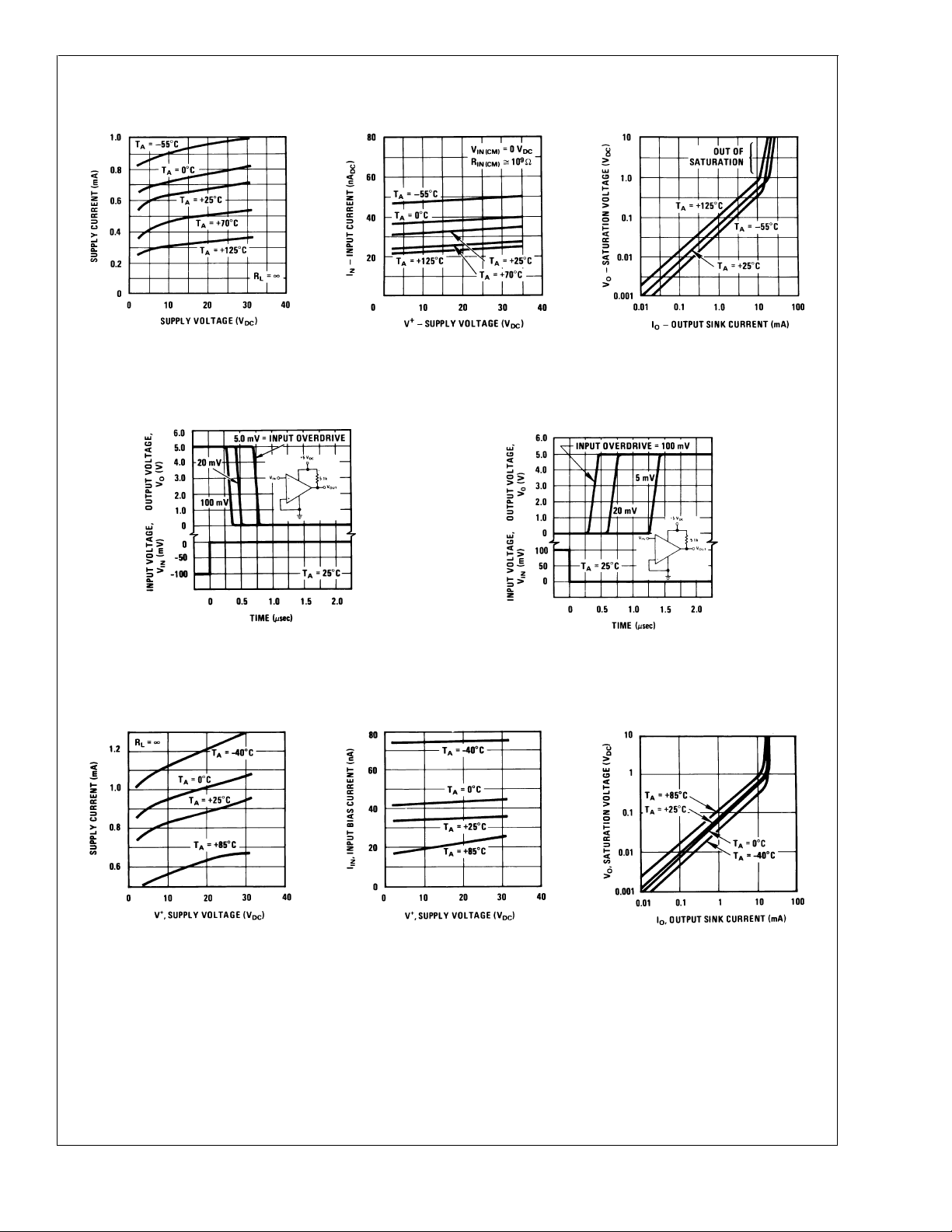
Typical Performance Characteristics LM139/LM239/LM339, LM139A/LM239A/LM339A, LM3302
LM139/LM239/LM339/LM2901/LM3302
Supply Current
Response Time for Various
Input Overdrives—Negative
Transition
DS005706-34
Input Current
Output Saturation Voltage
DS005706-35
Response Time for Various
Input Overdrives—Positive
Transition
DS005706-36
DS005706-37
Typical Performance Characteristics LM2901
Supply Current
DS005706-39
Input Current
DS005706-40
DS005706-38
Output Saturation Voltage
DS005706-41
www.national.com5
Typical Performance Characteristics LM2901 (Continued)
Response Time for Various
Input Overdrives—Negative
Transition
LM139/LM239/LM339/LM2901/LM3302
DS005706-42
Application Hints
The LM139 series are high gain, wide bandwidth devices
which, like most comparators, can easily oscillate if the
output lead is inadvertently allowed to capacitively couple to
the inputs via stray capacitance. This shows up only during
the output voltage transition intervals as the comparator
changes states. Power supply bypassing is not required to
solve this problem. Standard PC board layout is helpful as it
reduces stray input-output coupling. Reducing this input
resistors to
finally, adding even a small amount (1 to 10 mV) of positive
feedback (hysteresis) causes such a rapid transition that
oscillations due to stray feedback are not possible. Simply
socketing the IC and attaching resistors to the pins will cause
input-output oscillations during the small transition intervals
unless hysteresis is used. If the input signal is a pulse
waveform, with relatively fast rise and fall times, hysteresis is
not required.
All pins of any unused comparators should be tied to the
negative supply.
The bias network of the LM139 series establishes a drain
current which is independent of the magnitude of the power
supply voltage over the range of from 2 V
It is usually unnecessary to use a bypass capacitor across
the power supply line.
Typical Applications (V
<
10 kΩ reduces the feedback signal levels and
to 30 VDC.
DC
+
= 5.0 VDC)
Response Time for Various
Input Overdrives-Positive
Transition
DS005706-43
The differential input voltage may be larger than V
damaging the device. Protection should be provided to
prevent the input voltages from going negative more than
−0.3 V
(at 25˚C). An input clamp diode can be used as
DC
shown in the applications section.
The output of the LM139 series is the uncommitted collector
of a grounded-emitter NPN output transistor. Many collectors
can be tied together to provide an output OR’ing function. An
output pull-up resistor can be connected to any available
power supply voltage within the permitted supply voltage
range and there is no restriction on this voltage due to the
magnitude of the voltage which is applied to the V
of the LM139A package. The output can also be used as a
simple SPST switch to ground (when a pull-up resistor is not
used). The amount of current which the output device can
sink is limited by the drive available (which is independent of
+
V
) and the β of this device. When the maximum current limit
is reached (approximately 16 mA), the output transistor will
come out of saturation and the output voltage will rise very
rapidly. The output saturation voltage is limited by the
approximately 60Ω R
of the output transistor. The low
SAT
offset voltage of the output transistor (1 mV) allows the
output to clamp essentially to ground level for small load
currents.
+
without
+
terminal
Basic Comparator
DS005706-3
www.national.com 6
Driving CMOS
DS005706-4
Driving TTL
DS005706-5
 Loading...