

NSC LM3361AN Datasheet
August 1989
LM3361A Low Voltage/Power Narrow Band FM IF System
LM3361A Low Voltage/Power Narrow Band FM IF System
General Description
The LM3361A contains a complete narrow band FM demodulation system operable to less than 2V supply voltage.
Blocks within the device include an oscillator, mixer, FM IF
limiting amplifier, FM demodulator, op amp, scan control,
and mute switch. The LM3361A is similar to the MC3361
with the following improvements: the LM3361A has higher
voltage swing both at the op amp and audio outputs. It also
has lower nominal drain current and a squelch circuit that
draws significantly less current than the MC3361. Device
pinout functions are identical with some slightly different operating characteristics.
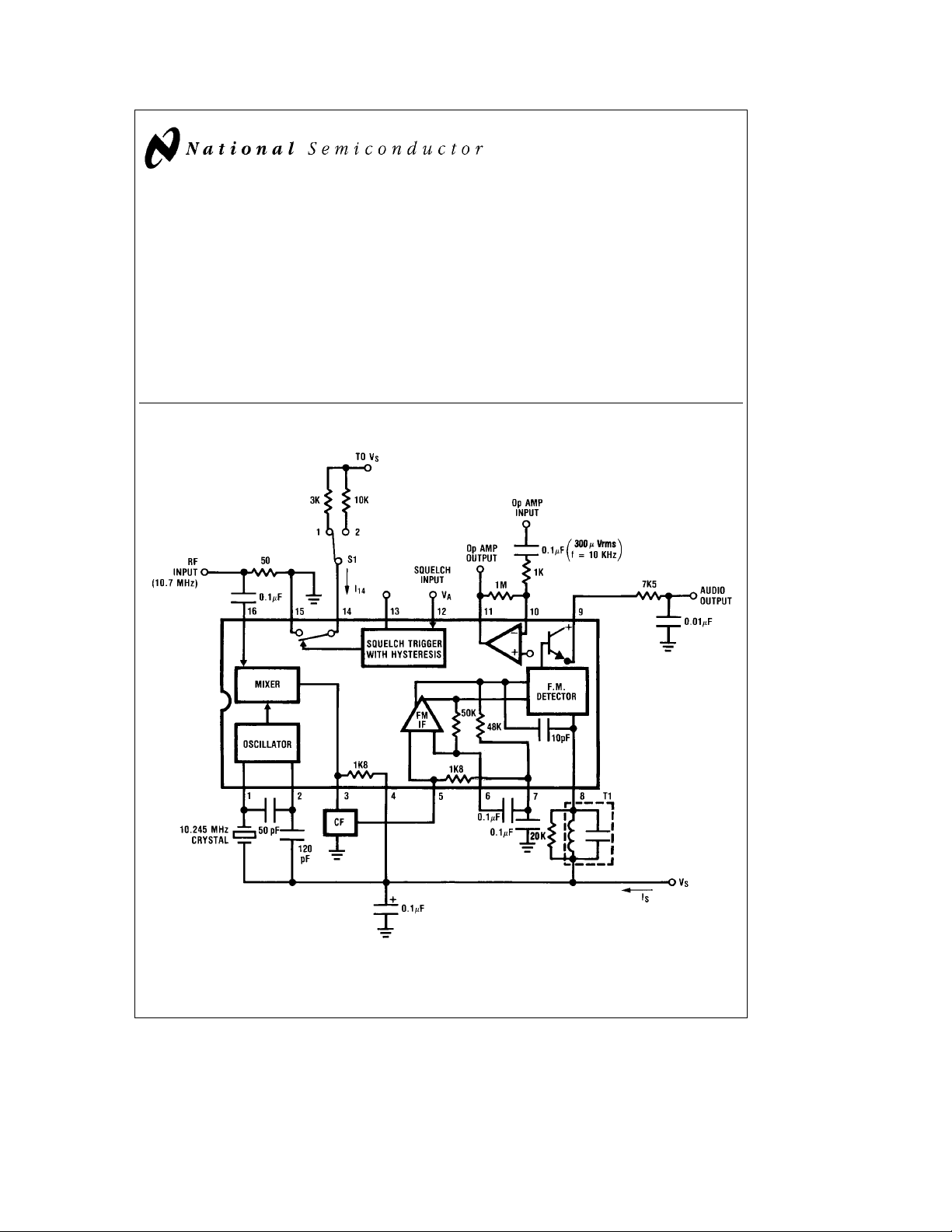
Block Diagram and Test Circuit
Features
Y
Functions at low supply voltage (less than 2V)
Y
Highly sensitive (b3 dB limiting at 2.0 mV input typical)
Y
High audio output (increased 6 dB over MC3361)
Y
Low drain current (2.8 mA typ., V
Y
Minimal drain current increase when squelched
Y
Low external parts count
CC
e
3.6V)
Order Number LM3661AM
or LM3361AN
T1-TOKO RMC-2A6597HM
CF-MURATA CFU 455E
TL/H/5586– 1
See NS Package Number
M16A or N16E
C
1995 National Semiconductor Corporation RRD-B30M115/Printed in U. S. A.
TL/H/5586
Absolute Maximum Ratings
If Military/Aerospace specified devices are required,
please contact the National Semiconductor Sales
Office/Distributors for availability and specifications.
Package Dissipation (Note 1) 1500 mW
Power Supply Voltage (V
RF Input Voltage (V
Mute Function (pin 14)
Operating Ambient Temperature Range 0§Ctoa70§C
Storage Temperature Range
)12V
S
l
3.6V) 1 Vrms
S
b
0.7 to 5 Vp
b
55§Ctoa150§C
Soldering Information
Dual-In-Line Package
Soldering (10 seconds) 260
Small Outline Package
Vapor Phase (60 seconds) 215
Infrared (15 seconds) 220
See AN-450 ‘‘Surface Mounting Methods and Their Effect
on Product Reliability’’ for other methods of soldering surface mount devices.
C
§
C
§
C
§
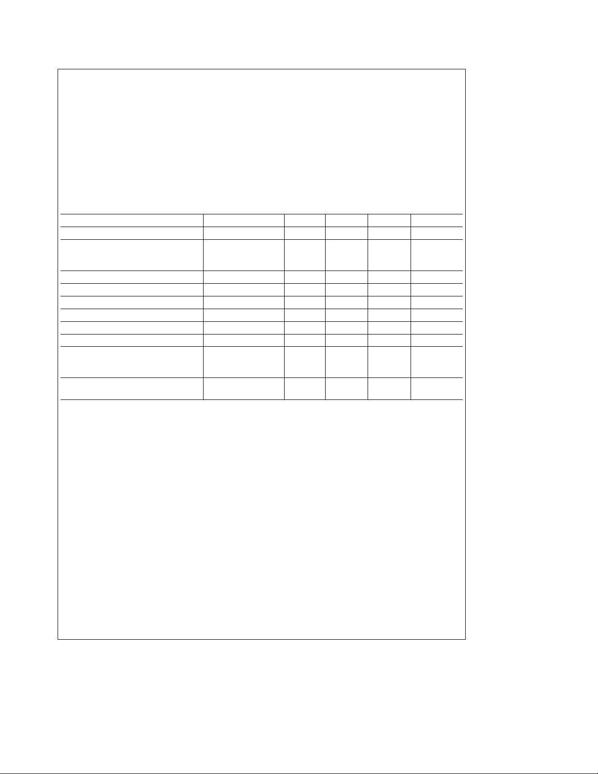
Parameters Guaranteed By Electrical Testing
(Test ckt., T
e
A
Supply Voltage Range V
Supply Current
Squelch Off I
Squelch On I
RF Input forb3 dB Limiting RF Input 2.0 6.0 mV
Recovered Audio at Audio Output Audio Output 200 350 mV
Audio Out DC V
Op Amp Gain V11/V
Op Amp Output DC V
Op Amp Input Bias Current (V
Scan Voltage
Pin 12 high (2V) V
Pin 12 Low (0V) V
Mute Switch Impedance, Pin 12e0V DV14/DI
Switch S1 from pos.1 to pos.2
25§C, V
e
S
3.6V, f
e
10.7 MHz, D f
O
e
g
3 kHz, f
e
1 kHz, 50X source)
MOD
Parameter Measure Min Typ Max Units
S
S
S
9
IN
10
b
V11)/1MX 20 75 nA
10
13
13
14
2.0 3.6 9.0 V
2.8 5.0 mA
3.6 6.0 mA
1.2 1.5 1.8 V
40 55 dB
0.4 0.7 V
0 0.5 V
3.0 3.4 V
15 30 X
RMS
DC
DC
DC
DC
Design Parameters Not Tested or Guaranteed
Mixer Conversion Gain (Note 2) 46 V/V
Mixer Input Resistance 3.6 kX
Mixer Input Capacitance 2.2 pF
Detector Output Impedance 500 X
Squelch Hysterisis 100 mV
Mute Off Impedance (measure pin 14 with pin 12
@
Squelch Threshold 0.65 V
Detector Center Frequency Slope 0.15 V/kHz
Note 1. For operation above 25§C ambient temperature, the device must be derated based on 150§C maximum junction temperature and a thermal resistance i
of 80§C/W.
Note 2. Mixer gain is supply dependent and effects overall sensitivity accordingly (See Typical Performance Characteristics).
Typ
2V) 10 MX
DC
JA
Coils:
Toko America
1250 Feehanville Drive
Mount Prospect, IL 60056
(312) 297-0070
Filters:
Murata
2200 Lake Park Drive
Smyrna, GA 30080
(404) 436-1300
2
 Loading...