

NSC LM2665M6, LM2665M6X Datasheet
LM2665
Switched Capacitor Voltage Converter
LM2665 Switched Capacitor Voltage Converter
November 1999
General Description
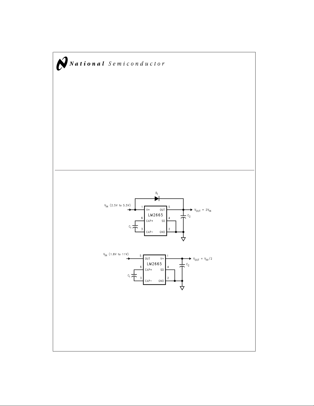
The LM2665 CMOS charge-pump voltage converter operates asa voltage doubler for an input voltage in the range of
+2.5V to +5.5V. Two low cost capacitors and a diode
(needed during start-up) are used in this circuit to provide up
to 40 mA of output current. The LM2665 can also work as a
voltage divider to split a voltage in the range of +1.8V to
+11V in half.
The LM2665 operates at 160 kHz oscillator frequency to reduce output resistance and voltage ripple. With an operating
current of only650 µA (operating efficiency greaterthan 90
with most loads) and 1µA typical shutdown current, the
LM2665 provides ideal performance for battery powered
systems. The device is in SOT-23-6 package.
Basic Application Circuits
Voltage Doubler
Splitting Vinin Half
Features
n Doubles or Splits Input Supply Voltage
n SOT23-6 Package
n 12Ω Typical Output Impedance
n 90%Typical Conversion Efficiency at 40 mA
n 1µA Typical Shutdown Current
Applications
n Cellular Phones
n Pagers
%
n PDAs
n Operational Amplifier Power Suppliers
n Interface Power Suppliers
n Handheld Instruments
DS100049-1
DS100049-2
© 1999 National Semiconductor Corporation DS100049 www.national.com
Absolute Maximum Ratings (Note 1)
If Military/Aerospace specified devices are required,
LM2665
please contact theNational Semiconductor Sales Office/
Distributors for availability and specifications.
Supply Voltage (V+ to GND, or GND to OUT) 5.8V
SD (GND − 0.3V) to (V+ +
V+ and OUT Continuous Output Current 50 mA
Output Short-Circuit Duration to GND (Note 2) 1 sec.
0.3V)
Continuous Power
Dissipation (T
T
(Note 3) 150˚C
JMax
θ
(Note 3) 210˚C/W
JA
Operating Junction
=
25˚C)(Note 3)
A
−40˚ to 85˚C
Temperature Range
Storage Temperature Range −65˚C to +150˚C
Lead Temp. (Soldering, 10 seconds) 300˚C
ESD Rating 2kV
Electrical Characteristics
Limits in standard typeface are for T
less otherwise specified: V+=5V, C
Symbol Parameter Condition Min Typ Max Units
V+ Supply Voltage 2.5 5.5 V
I
Q
I
SD
V
SD
I
L
R
SW
R
OUT
f
OSC
f
SW
P
EFF
V
OEFF
Note 1: Absolute maximum ratings indicate limits beyond which damage to the device may occur. Electrical specifications do not apply when operating the device
beyond its rated operating conditions.
Note 2: OUTmay be shorted to GND for onesecond without damage. However, shorting OUT to V+ may damage the device and should be avoided.Also, for temperatures above 85˚C, OUT must not be shorted to GND or V+, or device may be damaged.
Note 3: The maximum allowable power dissipation is calculated by using P
ambient temperature, and θ
Note 4: Inthetestcircuit, capacitors C
voltage and efficiency.
Note 5: The minimum input high for the shutdown pin equals 40%of V+.
Note 6: The maximum input low of the shutdown pin equals 20%of V+.
Note 7: Specifiedoutputresistance includes internal switch resistance and capacitor ESR. See thedetails in the application information for positive voltage doubler.
Note 8: The output switches operate at one half of the oscillator frequency, f
Supply Current No Load 650 1250 µA
Shutdown Supply Current 1 µA
Shutdown Pin Input Voltage Shutdown Mode 2.0
Output Current 40 mA
Sum of the R
internal MOSFET switches
ds(on)
Output Resistance (Note 7) I
Oscillator Frequency (Note 8) 80 160 kHz
Switching Frequency (Note 8) 40 80 kHz
Power Efficiency RL(1.0k) between GND and
Voltage Conversion Efficiency No Load 99 99.96
is the junction-to-ambient thermal resistance of the specified package.
JA
=
25˚C, and limits in boldface type apply over the full operating temperature range. Un-
J
=
=
C
3.3 µF. (Note 4)
1
2
(Note 5)
Normal Operation 0.8
(Note 6)
of the four
and C2are 3.3 µF, 0.3Ω maximum ESR capacitors. CapacitorswithhigherESRwillincreaseoutput resistance, reduce output
1
=
I
40 mA 3.5 8 Ω
L
=
40 mA 12 25 Ω
L
OUT
=
I
40 mA to GND 90
L
DMax
OSC
=
=
(T
JMax−TA
2f
SW
)/θJA, where T
.
86 93
is the maximum junction temperature, TAis the
JMax
600 mW
V
%
%
www.national.com 2
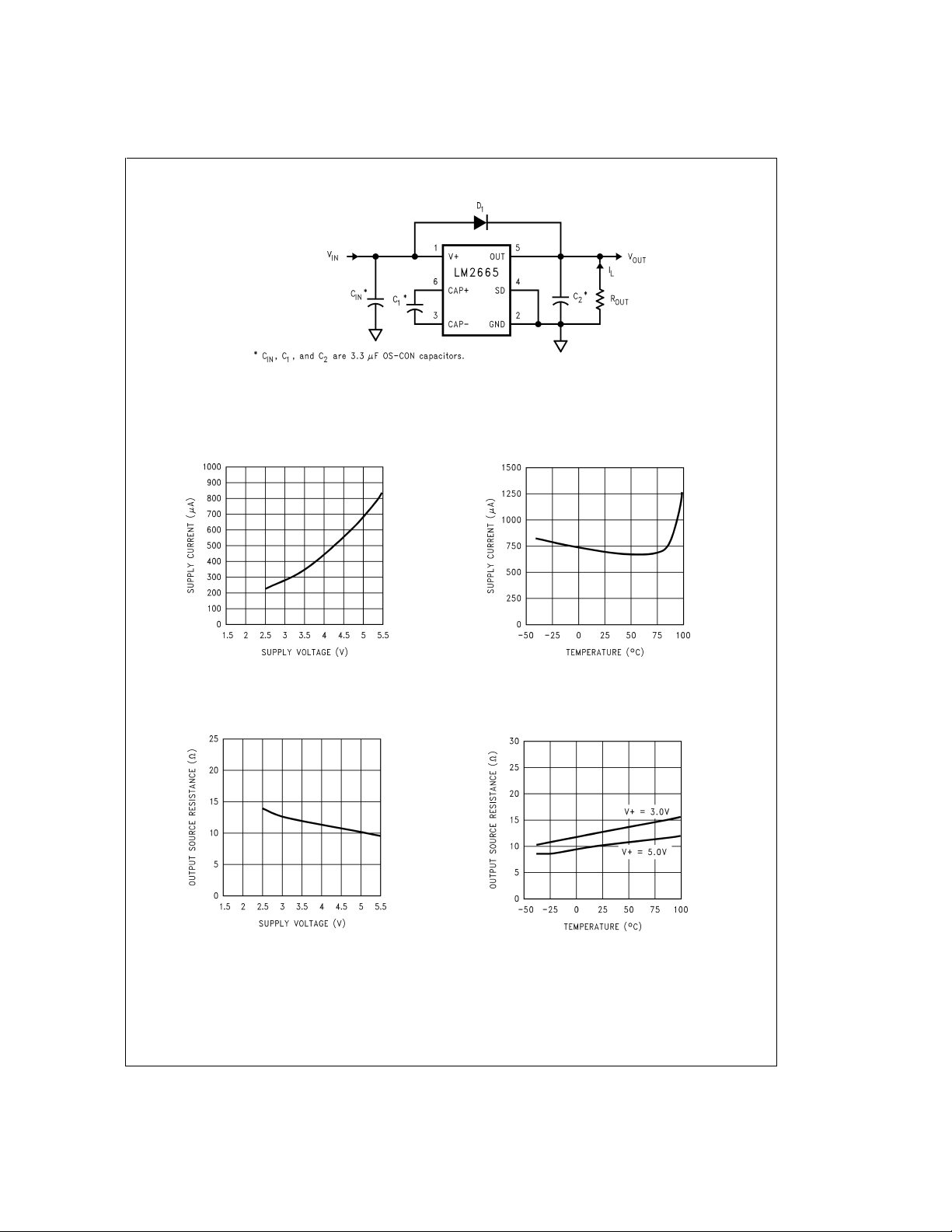
Test Circuit
FIGURE 1. LM2665 Test Circuit
Typical Performance Characteristics
LM2665
DS100049-3
(Circuit of Figure 1, V+=5V unless otherwise specified)
Supply Current vs
Supply Voltage
Output Source
Resistance vs Supply
Voltage
DS100049-4
Supply Current vs
Temperature
DS100049-5
Output Source
Resistance vs
Temperature
DS100049-6
DS100049-7
www.national.com3
 Loading...