NSC LM2653MTCX-ADJ, LM2653MTC-ADJ Datasheet

LM2653
1.5A High Efficiency Synchronous Switching Regulator
General Description
The LM2653 switching regulator provides high efficient
power conversion over a 100:1 load range (1.5A to 15 mA).
This feature makes the LM2653 an ideal fit in
battery-powered applications.
Synchronous rectification is used to achieve up to 97%efficiency.At lightloads, the LM2653enters a lowpower hysteretic or “sleep” mode to keep the efficiency high.In many applications, the efficiency still exceeds 80%at 15 mA load. A
shutdown pin is available to disable the LM2653 and reduce
the supply current to 7µA.
All the power, control, and drive functions are integrated
within the ICs.The ICs contain patented current sensing circuity forcurrent mode control. This featureeliminates the external current sensing resistor required by other
current-mode DC-DC converters.
The ICs have a 300 kHz fixed frequency internal oscillator.
The high oscillator frequency allows the use of extremely
small, low profile components.
Protection features include thermal shutdown, input undervoltage lockout, adjustable soft-start, cycle by cycle current
limit, output overvoltage and undervoltage protections.
Features
n Efficiency up to 97
%
n 4V to 14V input voltage range
n 1.5V to 5.0V adjustable output voltage
n 0.1Ω Switch On Resistance
n 300 kHz fixed frequency internal oscillator
n 7 µA shutdown current
n Patented current sensing for current mode control
n Input undervoltage lockout
n Output overvoltage shutdown protection
n Output undervoltage shutdown protection
n Adjustable soft-start
n Adjustable PGOOD delay
n Current limit and thermal shutdown
Applications
n Webpad
n Personal digital assistants (PDAs)
n Computer peripherals
n Battery-powered devices
n Notebook computer video supply
n Handheld scanners
n GXM I/O and core voltage
n High efficiency 5V conversion
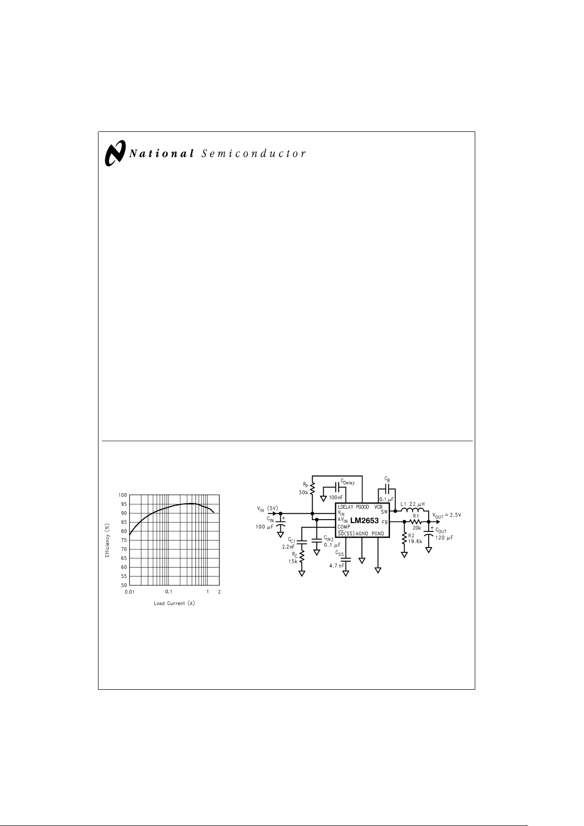
Typical Application
Efficiency vs Load Current
(V
IN
=
5V, V
OUT
=
3.3V)
DS101049-2
DS101049-30
November 1999
LM2653 1.5A High Efficiency Synchronous Switching Regulator
© 1999 National Semiconductor Corporation DS101049 www.national.com

Absolute Maximum Ratings (Note 1)
If Military/Aerospace specified devices are required,
please contactthe National Semiconductor Sales Office/
Distributors for availability and specifications.
Input Voltage 15V
PGOOD Pin Voltage 15V
Feedback Pin Voltage −0.4V ≤ V
FB
≤ 5V
Power Dissipation (T
A
=
25˚C),
(Note 2) 893 mW
Junction Temperature
Range −40˚C ≤ T
J
≤ +125˚C
Storage Temperature Range −65˚C to +150˚C
Lead Temperature
M Package
Vapor Phase (60 sec.) 215˚C
Infrared (15 sec.) 220˚C
Maximum Junction
Temperature
150˚C
ESD Susceptibility
Human Body Model (Note 3) 1 kV
Operating Ratings (Note 1)
Supply Voltage 4V ≤ V
IN
≤ 14V
Electrical Characteristics
Specifications with standard typeface are for T
J
=
25˚C, and those in boldface type apply over full Operating Temperature
Range.V
IN
=
10V unless otherwise specified.
Symbol Parameter Conditions
Typical
(Note 5)
Limit
(Note 4)
Units
V
FB
Feedback Voltage I
LOAD
=
900 mA 1.238
1.200
1.263
V
V(min)
V(max)
V
OUT
Output Voltage Line
Regulation
V
IN
=
4V to 12V
I
LOAD
=
900 mA
0.2
%
Output Voltage Load
Regulation
I
LOAD
=
10 mA to 1.5A
V
IN
=
5V
1.3
%
Output Voltage Load
Regulation
I
LOAD
=
200 mA to 1.5A
V
IN
=
5V
0.3
%
V
INUV
VINUndervoltage Lockout
Threshold Voltage
Rising Edge 3.8
3.95
V
V(max)
V
UV_HYST
Hysteresis for the Input
Undervoltage Lockout
210 mV
I
CL
Switch Current Limit V
IN
=
5V
V
OUT
=
2.5V
2.0
1.55
2.60
A
A(min)
A(max)
I
SM
Sleep Mode Threshold
Current
V
IN
=
5V, V
OUT
=
2.5V
100 mA
V
HYST
Sleep Mode Feedback
Voltage Hysteresis
24 mV
I
Q
Quiescent Current 1.7
2.0
mA
mA(max)
I
QSD
Quiescent Current in
Shutdown Mode
Shutdown Pin Pulled Low 7
12/20
µA
µA(max)
R
DS(ON)
High-Side or Low-Side
MOSFET ON Resistance
I
SWITCH
=1A 75
130
mΩ
mΩ (max)
R
SW(ON)
High-Side or Low-Side
Switch On Resistance
(MOSFET ON Resistance
+ Bonding Wire
Resitstance)
I
SWITCH
= 1A 110 mΩ
I
L
Switch Leakage
Current— High Side
130 nA
Switch Leakge
Current— Low Side
130 nA
V
BOOT
Bootstrap Regulator
Voltage
I
BOOT
= 1 mA 6.75
6.45/6.40
6.95/7.00
V
V(min)
V(max)
LM2653
www.national.com 2

Electrical Characteristics (Continued)
Specifications with standard typeface are for T
J
=
25˚C, and those in boldface type apply over full Operating Temperature
Range.V
IN
=
10V unless otherwise specified.
Symbol Parameter Conditions
Typical
(Note 5)
Limit
(Note 4)
Units
G
M
Error Amplifier
Transconductance
1250 µmho
A
V
Error Amplifier Voltage
Gain
100
I
EA_SOURCE
Error Amplifier Source
Current
VIN= 3.6V, VFB= 1.17V, V
COMP
=
2V
40
25/15
µA
µA(min)
I
EA_SINK
Error Amplifier Sink Current VIN= 3.6V, VFB= 1.31V, V
COMP
=
2V
65
30
µA
µA(min)
V
EAH
Error Amplifier Output
Swing Upper Limit
VIN= 4V, VFB= 1.17V 2.70
2.50/2.40
V
V(min)
V
EAL
Error Amplifier Output
Swing Lower Limit
VIN= 4V, VFB= 1.31V 1.25
1.35/1.50
V
V(max)
V
D
Body Diode Voltage I
DIODE
= 1.5A 1 V
F
OSC
Oscillator Frequency Measured at Switch Pin
V
IN
=4V
300
280/255
330/345
kHz
kHz(min)
kHz(max)
D
MAX
Maximum Duty Cycle VIN=4V 95
92
%
%
(min)
I
SS
Soft-Start Current Voltage at the SS Pin = 1.4V 11
7
14
µA
µA(min)
µA(max)
V
OUTUV
V
OUT
Undervoltage
Lockout Threshold Voltage
81
76
84
%
V
OUT
%
V
OUT
(min)
%
V
OUT
(max)
Hysteresis for V
OUTUV
5
%
V
OUT
V
OUTOV
V
OUT
Overvoltage Lockout
Threshold Voltage
108
106
114
%
V
OUT
%
V
OUT
(min)
%
V
OUT
(max)
Hysteresis for V
OUTOV
3
%
V
OUT
I
LDELAY__
SOURCE
LDELAY Pin Source
Current
5µA
I
PGOOD__SINK
PGOOD Pin Sink Current V
PGOOD
= 0.4V 15 mA(max)
I
PGOOD__LEAKAGE
PGOOD Pin Leakage
Current
V
PGOOD
=5V 50 nA
I
SHUTDOWN
Shutdown Pin Current Shutdown Pin Pulled Low 2.2
0.8/0.5
3.7/4.0
µA
µA(min)
µA(max)
V
SHUTDOWN
Shutdown Pin Threshold
Voltage
Rising Edge 0.6
0.3
0.9
V
V(min)
V(max)
T
SD
Thermal Shutdown
Temperature
165 ˚C
T
SD_HYST
Thermal Shutdown
Hysteresis Temperature
25 ˚C
Note 1: Absolute Maxmum Ratingsindicate limits beyond which damageto the device may occur. Operating Ratings indicate conditionsfor which the device is intended to be functional, but device parameter specifications may notbe guaranteed under these conditions.For guaranteed specifications and test conditions, see
the Electrical Characteristics.
Note 2: The maximum allowablepower dissipation is calculated by using P
DMAX
=
(T
JMAX−TA
)/θJA, whereT
JMAX
is themaximum junction temperature, TAis the
ambient temperature, and θ
JA
is the junction-to-ambient thermal resistance of the specified package. The 893 mW rating results from using 150˚C, 25˚C, and
140˚C/W forT
JMAX,TA
, and θJArespectively.A θJAof 140˚C/W represents the worst-case condition of no heat sinkingof the 16-pin TSSOP package.Heat sinking
allows the safe dissipation of more power.The Absolute Maximum power dissipationmust bederated by7.14 mWper ˚Cabove 25˚C ambient. The LM2653 actively
limits its junction temperatures to about 165˚C.
Note 3: The human body model is a 100 pF capacitor discharged through a 1.5 kΩ resistor into each pin.
LM2653
www.national.com3

Electrical Characteristics (Continued)
Note 4: Typical numbers are at 25˚C and represent the most likely norm.
Note 5: All limits guaranteed at room temperature (standard typeface) and at temperature extremes (bold typeface). All room temperature limits are 100%pro-
duction tested. Alllimits attemperature extremes are guaranteed viacorrelation usingstandard Statistical Quality Control (SQC) methods. All limits are used to calculate Average Outgoing Quality Level (AOQL).
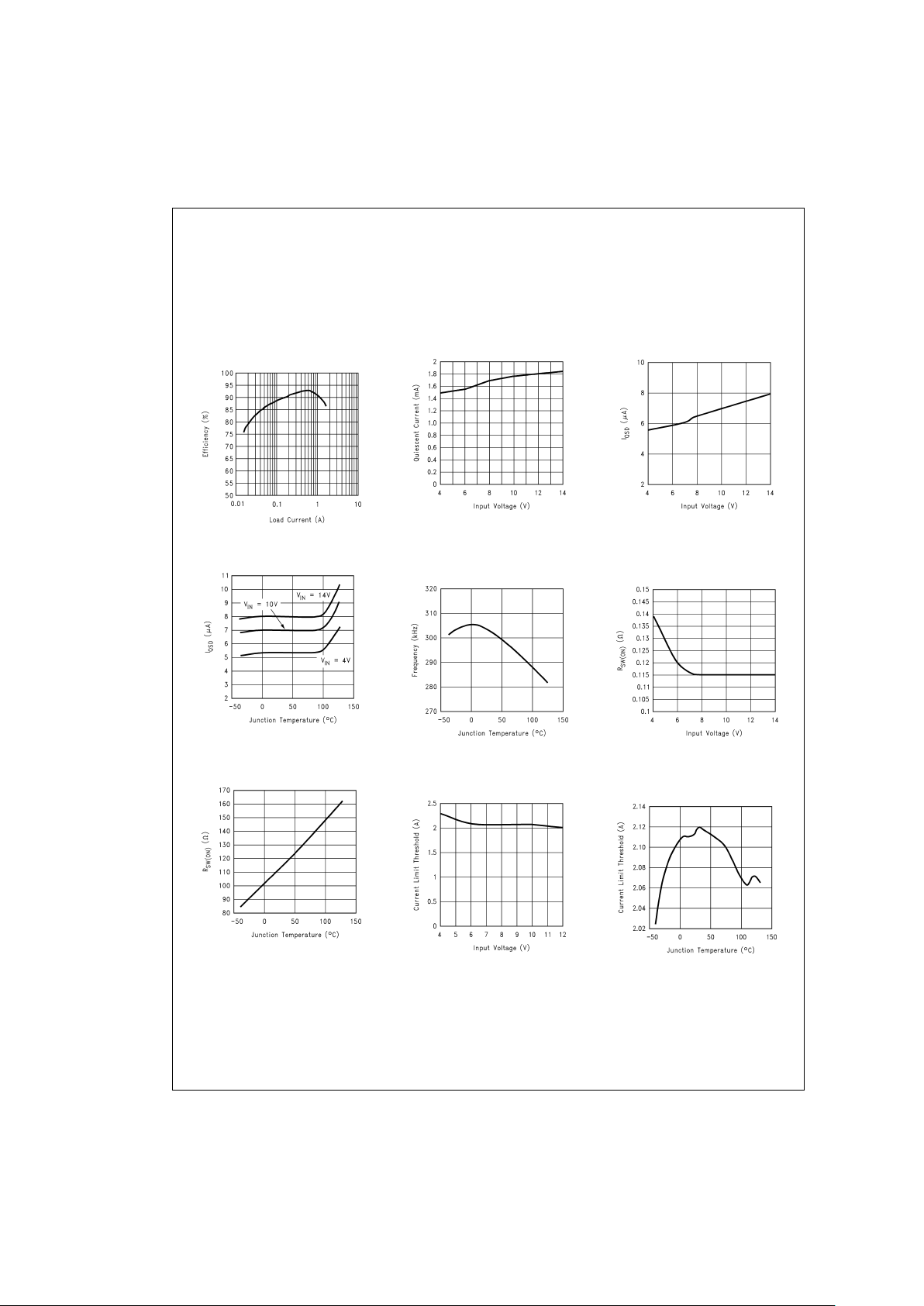
Typical Performance Characteristics
Efficiency vs Load Current
(V
IN
=
5V, V
OUT
=
2.5V)
DS101049-22
lQvs V
IN
DS101049-4
I
QSD
vs Input Voltage
DS101049-25
I
QSD
vs Junction Temperature
DS101049-26
Frequency vs Junction
Temperature
DS101049-7
R
SW(ON)
vs Input Voltage
DS101049-23
R
SW(ON)
vs Junction Temperature
DS101049-24
Current Limit vs Input Voltage
(V
OUT
=
2.5V)
DS101049-27
Current Limit vs Junction
Temperature (V
OUT
=
2.5V)
DS101049-28
LM2653
www.national.com 4
 Loading...