

LM1951 Solid State 1 Amp Switch
LM1951 Solid State 1 Amp Switch
August 1992
General Description
The LM1951 is a high current, high voltage, high side (PNP)
switch with a built-in error detection circuit.
The LM1951 is guaranteed to deliver 1 Amp output current
and is capable of withstanding up to
built-in error detection provides an error flag output under
the following fault conditions: output short to ground or supply, open load, current limit, overvoltage or thermal shutdown. The LM1951 will drive all types of resistive or inductive loads. The output has a built-in negative voltage clamp
&
b
(
30V) to provide a quick energy discharge path for
inductive loads. The LM1951 features TTL and CMOS compatible logic input with hysteresis. Switching times, both turn
on and turn off, are 2 ms(C
quiescent current in the OFF state is typically less than
load
0.1 mA at room temperature and less than 10 mA over the
entire operating temperature and voltage range.
The LM1951 features make it well suited for industrial and
automotive applications.
g
85V transients. The
k
0.005 mF). In addition, its
Features
Y
0.1 mA typical quiescent current (OFF state)
Y
1 Amp output current guaranteed
Y
g
85V transient protection
Y
Reverse voltage protection
Y
Negative output voltage clamp
Y
Error flag output
Y
Internal overvoltage shutdown
Y
Internal thermal shutdown
Y
Short circuit proof
Y
High speed switching (up to 50 kHz)
Y
Inductive or resistive loads
Y
Low ON resistance (1X maximum)
Y
TTL, CMOS compatible input with hysteresis
Y
Plastic TO-220 5-lead package
Y
ESD protected
Y
4.5V to 26V operation
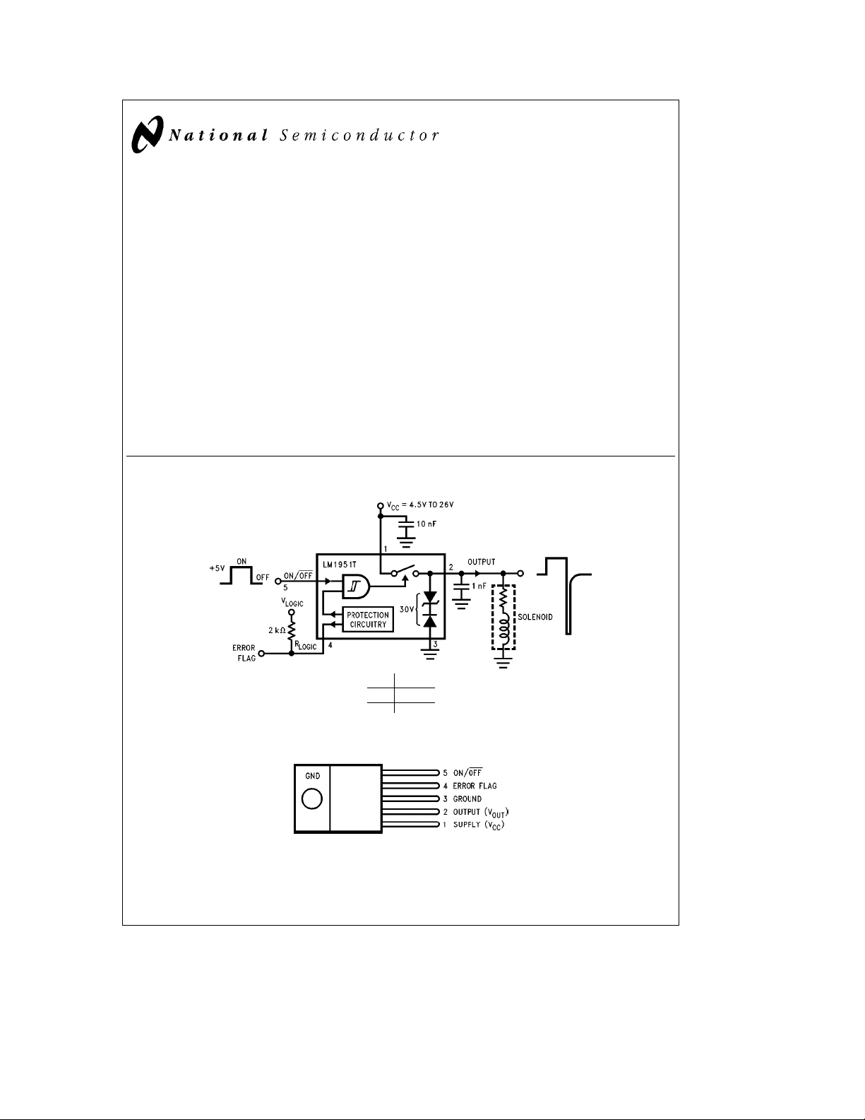
Typical Application Circuit and Connection Diagram
VINOutput
0 OFF
1ON
TL/H/9133– 1
TO-220, 5-Lead
Front View
TL/H/9133– 2
Order Number LM1951T
See NS Package Number T05A
C
1995 National Semiconductor Corporation RRD-B30M115/Printed in U. S. A.
TL/H/9133
Absolute Maximum Ratings
If Military/Aerospace specified devices are required,
please contact the National Semiconductor Sales
Office/Distributors for availability and specifications.
Supply Voltage
Operational Voltage 26 V
Sustained Voltage
Transient Voltage Protection
e
(
u
100 ms, 1% Duty Cycle, R
b
Pins 4, 5 26 V
40 V
S
t
V
DC
CC
t
10X)
DC
s
85 V
DC
g
85V
DC
Power Dissipation (Note 1) Internally Limited
Load Inductance 1H
Operating Temperature Range (TA)
b
40§Ctoa125§C
Maximum Junction Temperature 150§C
Storage Temperature Range
b
65§Ctoa150§C
Lead Temperature (Soldering, 10 sec.) 260
ESD Tolerance (Note 4): 2000V
C
§
Electrical Characteristics
e
V
CC
Parameter Conditions Typical Limit Limit Units
Supply Voltage, V
Supply Current I
Voltage Drop I
b
(V
CC
Short Circuit Current V
Input Threshold, Pin 5 4.5VsV
Input Current, Pin 5 0.8VsV
Output Clamp I
Delay td,ON R
Time td, OFF
Rise Time 13 ms
Fall Time 13 ms
Error Flag Characteristics:
Output Voltage Error Condition, Pin 4 Low, Sinking 10 mA 0.3 0.8 V
Sink Current Error Condition, Pin 4e0.3V 10 3 mA
Output Leakage Current No Error, Pin 4e26V 0.01 1 mA
Response Time V
Note 1: Thermal resistance junction-to-case is 3§C/W. Thermal resistance case-to-ambient is 50§C/W.
Note 2: Tested Limits are guaranteed and 100% production tested.
Note 3: Design Limits are guaranteed (but not 100% production tested) over the operating temperature and supply voltage range. These limits are not used to
calculate outgoing quality levels.
Note 4: Human body model, 100 pF discharged through a 1.5 kX resistor.
12V, I
out
e
500 mA, C
out
e
0.001 mF, T
e
25§C unless otherwise specified
A
Tested Design
(Note 2) (Note 3)
CC
4.5 V
Operational 26 V
Transient ue100 ms, 1% Duty Cycle, R
CC
t
10X
b
85 V
85 V
V
OUT
e
0 mA, V
out
e
I
250 mA, V
out
e
I
600 mA, V
out
e
I
1A, V
out
)
out
I
out
OUT
e
600 mA, V
e
1A, V
e
ON/OFF
ON/OFF
0V, V
e
ON/OFF
ON/OFF
0.8V 0.1 10 100 mA
e
ON/OFF
ON/OFF
ON/OFF
2.0V 260 270 mA
e
2.0V 630 650 mA
e
2.0V 1.06 1.2 A
e
2.0V 400 600 mV
e
2.0V 0.7 1.0 V
e
2V
1.3
1.0 A
2.5 A
s
26V Turn ON 1.4 2.0 2.0 V
CC
Turn OFF 1.2 0.8 0.8 V
s
ON/OFF
5.5V
25
50 mA
10 mA
out
load
s
600 mA
e
20X,C
b
e
0.001 mF13ms
load
b
30
40 V
b
24 V
13 ms
LOGIC
e
5V, R
LOGIC
e
2kX,C
e
0 mF1 ms
LOGIC
min
max
max
max
max
max
max
max
min
max
max
min
max
min
min
max
max
max
max
max
max
min
max
2
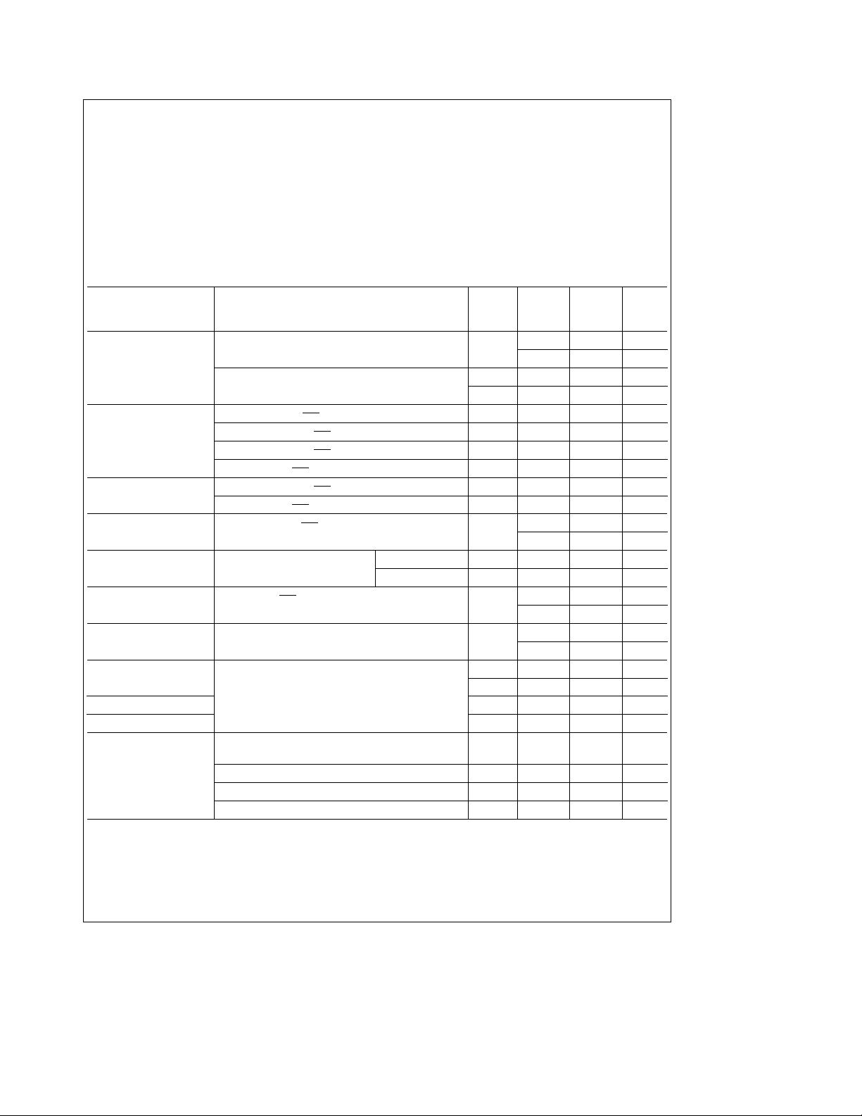
Typical Performance Characteristics
Quiescent Current Quiescent Current Voltage Drop
Voltage Drop Short Circuit Current High Voltage Behavior
Threshold (Pin 5) ON/OFF Current (Pin 5) ON/OFF Current (Pin 5)
ON/OFF
Output Voltage
Resistive Load
Output Voltage
Inductive Load
TL/H/9133– 3
3

Error Flag Output Characteristics
Open Load Threshold Open Load Threshold Over Voltage Threshold
Truth Table
TL/H/9133– 13
Fault Condition V
ON/OFF
* V
out
Error Flag
Normal L L H
HHH
Overvoltage L L L
HL L
Thermal Shutdown L L L
HL L
V
Short to GND L L H
OUT
HL L
V
OUT
Short to V
supply
LHL
HH L
Open Load L L H
HH L
Current Limit L L H
HH L
j
*L
0
s
V
ON/OFF
s
0.8V Hj2VsV
ON/OFF
s
26V
4

Typical Applications
FIGURE 1. Solenoid Actuated Valve
FIGURE 2. 60A 3-Phase Mercury Displacement Relay
TL/H/9133– 4
TL/H/9133– 5
*Available from Germanium Power Devices, Andover, MA, Tel. (617) 475-5982
FIGURE 3. 25A Switch with Short Circuit Foldback
5
TL/H/9133– 6

Typical Applications (Continued)
FIGURE 4. Latching Switch
FIGURE 5. Temperature Controller with Hysteresis
TL/H/9133– 7
TL/H/9133– 8
FIGURE 6. DC Motor Driver
6
TL/H/9133– 9

Typical Applications (Continued)
*
Operation Switch Type
Empty Normally Open
Fill Normally Closed
FIGURE 7. Over-Voltage Crowbar
TL/H/9133– 10
TL/H/9133– 11
FIGURE 8. Fluid Level Controller
FIGURE 9. Indicator Lamp Driver
7
TL/H/9133– 12

Application Hints
When inductive loads are turned OFF, they produce a negative voltage spike. The LM1951 contains a voltage clamp
that limits these spikes to approximately
ternal clamp is not necessary in most applications.
Loads with an inductance of greater than 1H, driven to full
output current, may damage the clamp simply by exceeding
the power capabilities of the LM1951. An LM1951 can dissipate 25W continuous at 25
large heatsink. If the load current is limited to 800 mA, the
C ambient when mounted on a
§
sustained spike from an infinitely large inductance can be
handled. Sustained spikes produced by higher currents and
high inductances will exceed the 25W limit.
For inductances above 1H, care should be taken to see that
the output current does not exceed a value that could damage the clamp. While 800 mA is acceptable for the device
running at 25
for smaller heatsinks or higher ambient temperatures to limit
the junction temperature to 150
clamp or resonating capacitor can be added to handle any
C ambient on a heatsink, derate this current
§
§
combination of load inductance, load current, and device
temperature. This is especially important if the output current is boosted, such as the application shown in
peak power of 750W could be developed in the internal
clamp if an inductive load is switched without external
clamping.
Another case where the clamp’s power capability may be
exceeded is when driving a solenoid. The inductance of a
solenoid is greatest when energized, with the plunger pulled
in. As the plunger is pulled out of the solenoid, the inductance goes down. Under certain conditions of high solenoid
inductance and fast mechanical time constants, the current
may actually increase when the solenoid is turned OFF.
Since the energy stored in an inductor cannot change instantaneously, the current must increase to conserve energy when the inductance decreases. This condition is traced
by observing the load current with a current probe and storage oscilloscope.
Load capacitances larger than 1 nF will slow rise and fall
times. Inductive loads having a capacitive component larger
than 1 nF will also exhibit overshoot. Furthermore, ringing
b
30V, thus an ex-
C. Alternatively, an external
Figure 3
.A
may be evident in a combination inductive/capacitive load,
or in an inductive load with supply decoupling capacitors in
the range of 100 nF to 1 m F. For fast rise and fall times and
minimum ringing with inductive loads, a supply decoupling
capacitor of 10 nF and an output capacitor of 1 nF is recommended. These should be located as close to the IC pins as
possible.
The error flag is an open collector output that pulls low under certain fault conditions. These errors include overvoltage (V
(I
circuit to supply, and junction temperature greater than
150
output to a 5V supply a logic output to a microprocessor is
l
26V), overcurrent (I
CC
k
2 mA), output short circuit to ground, output short
OUT
C. By connectinga2kXresistor from the error flag
§
l
1.3A), undercurrent
OUT
provided.
The error flag can give seemingly false indications in a number of situations. Slewing large capacitive loads (
l
100 nF)
can drive the LM1951 into temporary current limit, producing a momentary error indication. Incandescent lamps and
DC motors require an inrush current that will also cause a
temporary current limit and error indication. Large inductive
l
loads (
50 mH) initially appear as open circuits, falsing the
error flag. The error flag pulses for about 1 ms when any
load is turned ON since the output is initially at ground. In
microprocessor systems these false indications are easily
ignored in software. In discrete logic circuits utilizing a latch
at the error flag output, some filtering may be required.
An internal current sink (10 mA minimum) is connected to
the input, pin 5. If this pin is left open it is guaranteed to pull
low, switching the LM1951 OFF. This characteristic is important under certain fault conditions such as when the control line fails open cirucit.
Although the input threshold has hysteresis, the switch
points are derived from a very stable band-gap reference. In
many applications, such as
Figures 5
and7, the LM1951
input can replace an extenal reference and comparator.
The input (pin 5) is clamped at
b
0.7V and includes a series
resistance of approximately 30 kX. This pin tolerates negative inputs of up to 1 mA without affecting the performance
of the chip.
8

9
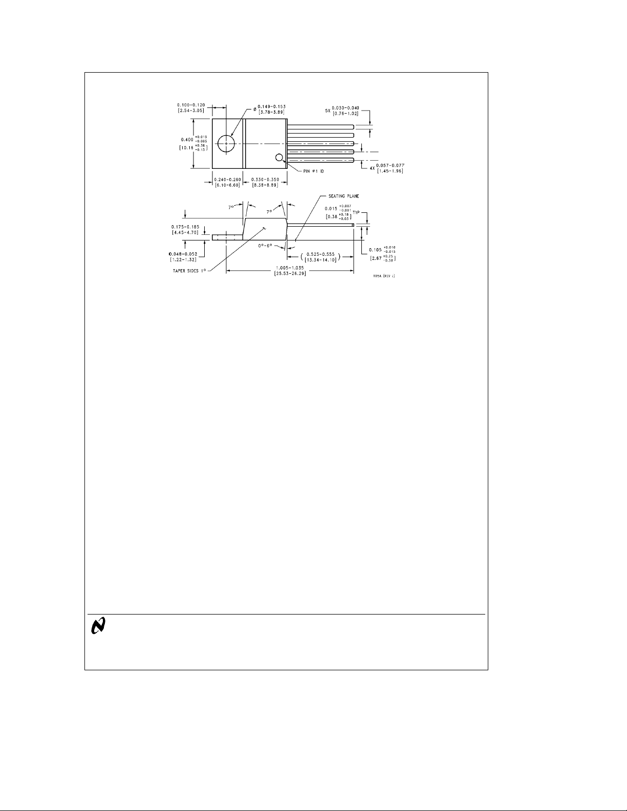
Physical Dimensions inches (millimeters)
LM1951 Solid State 1 Amp Switch
Outline Drawing
Order Number LM1951T
NS Package Number T05A
LIFE SUPPORT POLICY
NATIONAL’S PRODUCTS ARE NOT AUTHORIZED FOR USE AS CRITICAL COMPONENTS IN LIFE SUPPORT
DEVICES OR SYSTEMS WITHOUT THE EXPRESS WRITTEN APPROVAL OF THE PRESIDENT OF NATIONAL
SEMICONDUCTOR CORPORATION. As used herein:
1. Life support devices or systems are devices or 2. A critical component is any component of a life
systems which, (a) are intended for surgical implant support device or system whose failure to perform can
into the body, or (b) support or sustain life, and whose be reasonably expected to cause the failure of the life
failure to perform, when properly used in accordance support device or system, or to affect its safety or
with instructions for use provided in the labeling, can effectiveness.
be reasonably expected to result in a significant injury
to the user.
National Semiconductor National Semiconductor National Semiconductor National Semiconductor
Corporation Europe Hong Kong Ltd. Japan Ltd.
1111 West Bardin Road Fax: (
Arlington, TX 76017 Email: cnjwge@tevm2.nsc.com Ocean Centre, 5 Canton Rd. Fax: 81-043-299-2408
Tel: 1(800) 272-9959 Deutsch Tel: (
Fax: 1(800) 737-7018 English Tel: (
National does not assume any responsibility for use of any circuitry described, no circuit patent licenses are implied and National reserves the right at any time without notice to change said circuitry and specifications.
Fran3ais Tel: (
Italiano Tel: (
a
49) 0-180-530 85 86 13th Floor, Straight Block, Tel: 81-043-299-2309
a
49) 0-180-530 85 85 Tsimshatsui, Kowloon
a
49) 0-180-532 78 32 Hong Kong
a
49) 0-180-532 93 58 Tel: (852) 2737-1600
a
49) 0-180-534 16 80 Fax: (852) 2736-9960
 Loading...