

NSC LM1881MX, LM1881M, LM1881N Datasheet

TL/H/9150
LM1881 Video Sync Separator
February 1995
LM1881 Video Sync Separator
General Description
The LM1881 Video sync separator extracts timing information including composite and vertical sync, burst/back porch
timing, and odd/even field information from standard negative going sync NTSC, PAL*, and SECAM video signals with
amplitude from 0.5V to 2V p-p. The integrated circuit is also
capable of providing sync separation for non-standard, faster horizontal rate video signals. The vertical output is produced on the rising edge of the first serration in the vertical
sync period. A default vertical output is produced after a
time delay if the rising edge mentioned above does not occur within the externally set delay period, such as might be
the case for a non-standard video signal.
Features
Y
AC coupled composite input signal
Y l
10 kX input resistance
Y k
10 mA power supply drain current
Y
Composite sync and vertical outputs
Y
Odd/even field output
Y
Burst gate/back porch output
Y
Horizontal scan rates to 150 kHz
Y
Edge triggered vertical output
Y
Default triggered vertical output for non-standard video
signal (video games-home computers)
Connection Diagram
LM1881N
TL/H/9150– 1
Order Number LM1881M or LM1881N
See NS Package Number M08A or N08E
*PAL in this datasheet refers to European broadcast TV standard ‘‘Phase Alternating Line’’, and not to Programmable Array Logic.
C
1995 National Semiconductor Corporation RRD-B30M115/Printed in U. S. A.
Absolute Maximum Ratings
If Military/Aerospace specified devices are required,
please contact the National Semiconductor Sales
Office/Distributors for availability and specifications.
Supply Voltage 13.2V
Input Voltage 3 Vpp (V
CC
e
5V)
6 Vpp (V
CC
t
8V)
Output Sink Currents; Pins 1, 3, 5 5 mA
Output Sink Current; Pin 7 2 mA
Package Dissipation (Note 1) 1100 mW
Operating Temperature Range 0
§
Cb70§C
Storage Temperature Range
b
65§Ctoa150§C
ESD Susceptibility (Note 2) 2 kV
Soldering Information
Dual-In-Line Package (10 sec.) 260
§
C
Small Outline Package
Vapor Phase (60 sec.) 215
§
C
Infrared (15 sec.) 220
§
C
See AN-450 ‘‘Surface Mounting Methods and their Effect on
Product Reliability’’ for other methods of soldering surface
mount devices.
Electrical Characteristics
V
CC
e
5V; Rsete680 kX;T
A
e
25§C; Unless otherwise specified
Parameter Conditions Typ
Tested Design Units
Limit (Note 3) Limit (Note 4) (Limits)
Supply Current Outputs at Logic 1 V
CC
e
5V 5.2 10 mAmax
V
CC
e
12V 5.5 12 mAmax
DC Input Voltage Pin 2
1.5
1.3 Vmin
1.8 Vmax
Input Threshold Voltage Note 5
70
55 mVmin
85 mVmax
Input Discharge Current Pin 2; V
IN
e
2V
11
6 mAmin
16 mAmax
Input Clamp Charge Current Pin 2; V
IN
e
1V 0.8 0.2 mAmin
R
SET
Pin Reference Voltage Pin 6; Note 6
1.22
1.10 Vmin
1.35 Vmax
Composite Sync. & Vertical I
OUT
e
40 mA; V
CC
e
5V 4.5 4.0 Vmin
Outputs Logic 1 V
CC
e
12V 11.0 Vmin
I
OUT
e
1.6 mA V
CC
e
5V 3.6 2.4 Vmin
Logic 1 V
CC
e
12V 10.0 Vmin
Burst Gate & Odd/Even I
OUT
e
40 mA; V
CC
e
5V 4.5 4.0 Vmin
Outputs Logic 1 V
CC
e
12V 11.0 Vmin
Composite Sync. Output I
OUT
eb
1.6 mA; Logic 0; Pin 1 0.2 0.8 Vmax
Vertical Sync. Output I
OUT
eb
1.6 mA; Logic 0; Pin 3 0.2 0.8 Vmax
Burst Gate Output I
OUT
eb
1.6 mA; Logic 0; Pin 5 0.2 0.8 Vmax
Odd/Even Output I
OUT
eb
1.6 mA; Logic 0; Pin 7 0.2 0.8 Vmax
Vertical Sync Width 230 190 msmin
300 msmax
Burst Gate Width 2.7 kX from Pin 5 to V
CC
4
2.5 msmin
4.7 msmax
Vertical Default Time Note 7
65
32 msmin
90 msmax
Note 1: For operation in ambient temperatures above 25§C, the device must be derated based on a 150§C maximum junction temperature and a package thermal
resistance of 110
§
C/W, junction to ambient.
Note 2: ESD susceptibility test uses the ‘‘human body model, 100 pF discharged through a 1.5 kX resistor’’.
Note 3: Typicals are at T
J
e
25§C and represent the most likely parametric norm.
Note 4: Tested Limits are guaranteed to National’s AOQL (Average Outgoing Quality Level).
Note 5: Relative difference between the input clamp voltage and the minimum input voltage which produces a horizontal output pulse.
Note 6: Careful attention should be made to prevent parasitic capacitance coupling from any output pin (Pins 1, 3, 5, and 7) to the R
SET
pin (Pin 6).
Note 7: Delay time between the start of vertical sync (at input) and the vertical output pulse.
2
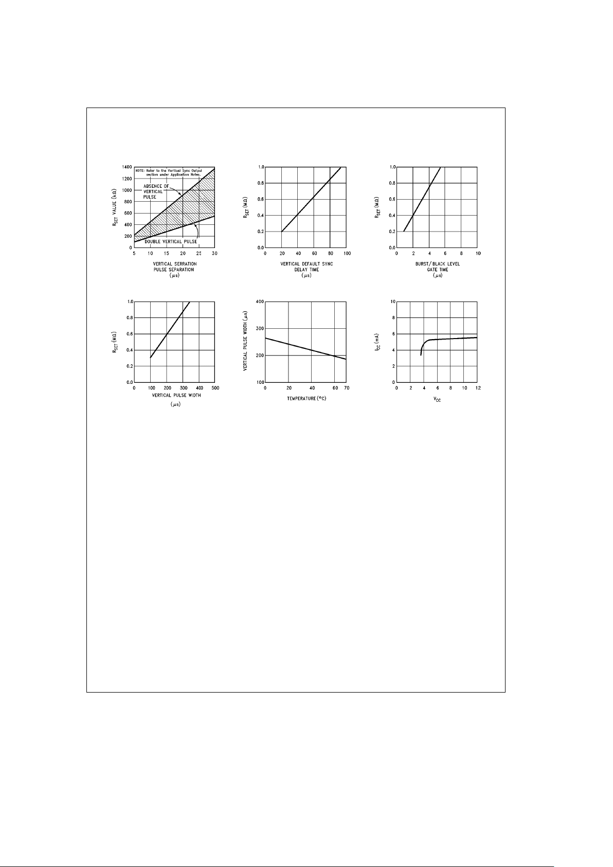
Typical Performance Characteristics
Pulse Separation
vs Vertical Serration
R
set
Value Selection
vs Rset
Sync Delay Time
Vertical Default
Gate Time vs Rset
Burst/Black Level
Width vs Rset
Vertical Pulse
Width vs Temperature
Vertical Pulse
Supply Voltage
Supply Current vs
TL/H/9150– 2
3
 Loading...