

TL/H/7912
LM1872 Radio Control Receiver/Decoder
February 1989
LM1872 Radio Control Receiver/Decoder
General Description
The LM1872 is a complete RF receiver/decoder for radio
control applications. The device is well suited for use at either 27 MHz, 49 MHz or 72 MHz in controlling various toys
or hobby craft such as cars, boats, tanks, trucks, robots,
planes, and trains. The crystal controlled superhet design
offers both good sensitivity and selectivity. When operated
in conjunction with the companion transmitter, LM1871, it
provides four independent information channels. Two of
these channels are analog pulse width modulated (PWM)
types, while the other two are simple ON/OFF digital channels with 100 mA drive capability. Either channel type can
be converted to the other form through simple external circuitry such that up to 4 analog or up to 4 digital channels
could be created. Few external parts are required to complement the self-contained device which includes local oscillator, mixer, IF detector, AGC, sync output drivers, and all
decoder logic on-chip.
Features
Y
Four independent information channels; two analog and
two digital
Y
Completely self-contained
Y
Minimum of external parts
Y
Operation from 50 kHz to 72 MHz
Y
Highly selective and sensitive superhet design
Y
Operates from four 1.5V cells
Y
Excellent supply noise rejection
Y
100 mA digital output drivers
Y
Crystal controlled
Y
Interfaces directly with standard hobby servos
Applications
Y
Toys and hobby craft
Y
Energy saving, remotely switched lighting systems
Y
Burgler alarms
Y
Industrial and consumer remote data links
Y
IR data links
Y
Remote slide projector control
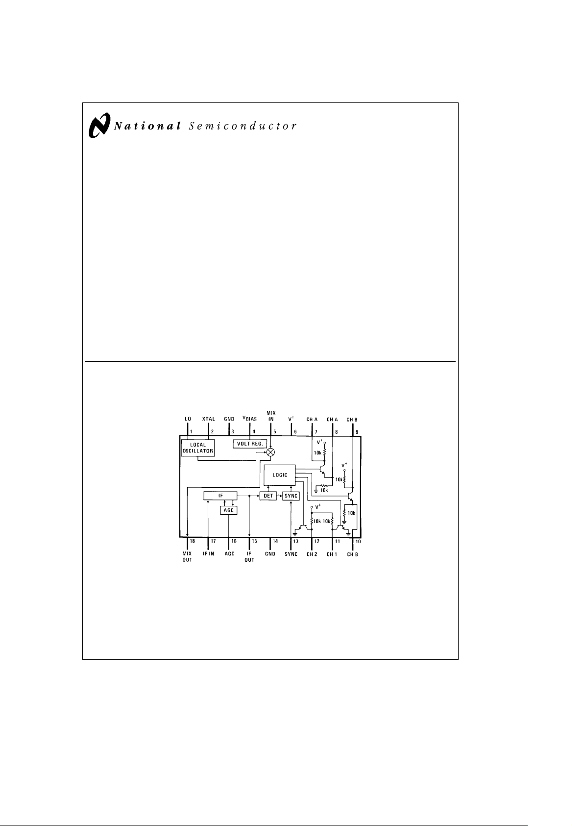
Circuit Block and Connection Diagram
Dual-In-Line Package
TL/H/7912– 1
Bottom View
Order Number LM1872N
See NS Package Number N18A
C
1995 National Semiconductor Corporation RRD-B30M115/Printed in U. S. A.

Absolute Maximum Ratings
If Military/Aerospace specified devices are required,
please contact the National Semiconductor Sales
Office/Distributors for availability and specifications.
Supply Voltage 7V
Package Dissipation (Note 2) 1600 mW
Voltage
@
Pin 7, 8, 9, 10, 11 or 12 V
a
Operating Temperature Range
b
25§Ctoa85§C
Storage Temperature Range
b
65§Ctoa150§C
Lead Temperature (Soldering, 10 sec.) 260§C
DC Electrical Characteristics
V
a
e
6V, T
A
e
25§C, Test Circuit of
Figure 1
,f
L0
e
49.890 MHz, f
IF
e
455 kHz unless otherwise specified
Parameter Conditions Min Typ Max Units
Supply Voltage Functional for V
IN
e
100 mV 2.5 6 7 V
Supply Current CHA&BOff 9 13 18 mA
CHA&BOn
27 mA
V
BIAS
@
Pin 4 1.85 2.1 2.35 V
Sync Timer Threshold
@
Pin 13, Going from
V
a
/2b0.4 Va/2 Va/2a0.3 V
Low to High Voltage
DIGITAL CHANNELS A AND B
Saturation Voltage
@
Pins7&9,R
L
e
100X 0.4 0.7 V
Saturation Resistance
@
Pins7&9 7 X
Source Current
@
Pins 8 & 10,
100 mA
V
Pin 8 & Pin 10
s
1V
Collector Pull-Up Pin7&Pin9toV
a
51020kX
Resistance
Emitter Pull-Down Pin 8 & Pin 10 to GND
51020kX
Resistance
ANALOG CHANNELS 1 AND 2
Saturation Voltage
@
Pins 11 & 12, R
L
e
2kX 0.45 0.7 V
Saturation Resistance
@
Pins 11 & 12 160 X
Collector Pull-Up Pin 11 & Pin 12 to V
a
51020kX
Resistance
AC Electrical Characteristics
Parameter Conditions Min Typ Max Units
RF Sensitivity For ‘‘Solid’’ Decoded Outputs
22 39 mV
(Note 1)
RF Sensitivity Circuit of
Figure 5
@
49 MHz
with Antenna Simulation 12 mV
Network of
Figure 6
Voltage Gain Pin 5 to Pin 15 58 dB
PSRR of RF Sensitivity 3VsV
a
s
6V
b
1%D/V
BW 3 dB Down@Pin 15 3.2 kHz
Noise Referred to Input, Pin 5, V
IN
e
0 0.35 mVrms
Referred to IF, Pin 15, V
IN
e
0 0.28 mVrms
AGC Threshold Onset of AGC Relative to
88 mV
RF Input, VIN,@Pin 5
Relative to IF Output@Pin 15 V
a
a
0.07 V
a
a
0.100 V
a
a
0.13 V
Mixer Conversion From Pin 5 to Pin 18
@
1 MHz 2.9 4.0 6.9 mmhos
Transconductance
@
27 MHz 3.7 mmhos
@
49 MHz 3.5 mmhos
2

AC Electrical Characteristics (Continued)
Parameter Conditions Min Typ Max Units
Mixer Input Impedance Pin 5 to Pin 4@49 MHz
20 kX
a
5pF
(See Curves)
Mixer Output Impedance Pin 18 to GND 250 kX
IF Transconductance Pin 17 to Pin 15 (AGC Off)@455 kHz 2.6 4.1 5.6 mmhos
IF Input Impedance Pin 17 to GND 5500 X
IF Output Impedance Pin 15 to GND (AGC Off) 800 kX
(AGC On) 2 MX
IF Carrier Level
@
Pin 15, V
IN
e
100 mV
70 mVrms
(AGC On)
Detector Threshold Relative to RF Input,
20 mV
V
IN
,@Pin 5
Relative to IF Output@Pin 15 V
a
a
0.015 V
a
a
0.025 V
a
a
0.040 V
Analog Pulse Width Ratio of Received Pulse Width
Accuracy
@
Pins 11 & 12 to Transmitted
0.95 1.0 1.05 ms/ms
Pulse Width
@
Pin 5 for
V
IN
e
100 mV
Note 1: The criteria for the outputs to be considered ‘‘solid’’ are as follows:
DIGITAL: In order to check the decoding section, four RF frames are inputted in sequence with the proper codes to exercise all four possible logical
output combinations at pins 7 and 9. For each frame the proper output logic state must exist.
ANALOG: Each analog pulse width (measured at pins 11 & 12) in any of the above four successive frames must not vary more than
g
5% from the pulse
widths obtained for V
IN
e
100 mV.
Note 2: For operation in ambient temperatures above 25
§
C, the device must be derated based on a 150§C maximum junction temperature and a package
thermal resistance of 75
§
C/W, junction to ambient.
Typical Performance Characteristics
Supply Voltage
Supply Current vs
Voltage vs Load Current
Analog Channel Output
vs Load Current
Collector Output Voltage
Digital Channel
Sensitivity vs Supply Voltage vs Input Frequency
Mixer Transconductance (g
m
)
Input Signal Level
IF Output Signal Level vs RF
TL/H/7912– 2
3

Typical Performance Characteristics (Continued)
IF Bandpass Response vs Frequency
Resistance and Capacitance
Equivalent Mixer Input Shunt
vs RF Input Level
Receiver AM Rejection
TL/H/7912– 3
Test Circuit
TL/H/7912– 4
Bottom View
L1eToko* 10k type (KEN-4028 DZ); 6T T2eToko* 10 EZC type (RMC 402503 NO), Que110
T1
e
Toko* 10 EZC type (RMC 202313 NO), Que110 Pin 1 –2, 98T; pin 2– 3, 66T
Pin 1 –2, 131T; pin 2– 3, 33T Pin 1 –3, 164T; pin 4– 6, 8T
Pin 1 –3, 164T; pin 4– 6, 5T
*Toko America
1250 Feehanville Drive
Mount Prospect, IL 60056
(312) 297-0070
FIGURE 1. Test Circuit
4
Circuit Description
The following discussion is best understood by referring to
Figures 2, 3, 4,
and5.
SYSTEM ENCODING AND DECODING SCHEME
For the transfer of analog information, the LM1871/LM1872
system uses conventional pulse width modulation (PWM). In
applying this technique, the RF carrier is interrupted for
short fixed intervals (t
M
in
Figure 2
) with each interval fol-
lowed by variable width pulses (t
CH
) so as to define multiple
variable time spans (t
M
a
tCH) occurring in serial fashion.
Synchronization is accomplished by allowing one of the
transmitted variable pulse widths (t
SYNC
) to exceed the du-
ration (t’
SYNC
) of a receiver-based timer, thus allowing the
receiver to recognize this pulse for synchronization purposes. Taken in sequence, this collection of pulses constitutes
a single frame period (t
F
).
The LM1871 transmitter is equipped to transmit up to
six
channels which the companion LM1872 receiver uses to
derive 2 analog and 2 digital channels. The receiver decodes the demodulated RF waveform from the transmitter
by negative edge triggering a cascade of three binary dividers called the A, B, and C toggle flip-flops (
Figure 4
). By
‘‘examining’’ all three flip-flop outputs simultaneously, up to
6 unique channel time intervals could be identified and recovered. Only the first two channels are actually decoded
however and outputted by the receiver, the rest being used
for identification of two digital (ON/OFF) channels. In passing digital information, a pulse count modulation scheme is
used whereby different quantities of channel pulses are
transmitted by varying the number of fixed width channels
following the two variable width analog channels 1 and 2
(see
Figure 3
).
TL/H/7912– 5
FIGURE 2. RX Timing Waveforms
LM1871 TX LM1872 RX
Pin Conditions Transmitted Waveform Binary Digital Outputs
Pin 5 (CH A) Pin 6 (CH B)
Pulse Count
CH A CH B
OPEN OPEN 100 OFF OFF
TL/H/7912– 6
GND OPEN 101 ON OFF
TL/H/7912– 7
OPEN GND 110 OFF ON
TL/H/7912– 8
GND GND 111 ON ON
TL/H/7912– 9
FIGURE 3. Digital Channel Encoding and Decoding via Pulse Count Modulation
5

Circuit Description (Continued)
TL/H/7912– 10
*External parts
²
Depending on layout, a small capacitance (10 –47 pF)
may be required across pins 2 and 3 to ensure
oscillator start up.
FIGURE 4. Simplified Schematic Diagram
6
 Loading...