

NSC LM1863M Datasheet
LM1863 AM Radio System for
Electronically Tuned Radios
General Description
The LM1863 is a high performance AM radio system intended primarily for electronically tuned radios. Important to this
application is an on-chip stop detector circuit which allows
for a user adjustable signal level threshold and center frequency stop window. The IC uses a low phase noise, levelcontrolled local oscillator.
Low phase noise is important for AM stereo which detects
phase noise as noise in the L-R channel. A buffered output
for the local oscillator allows the IC to directly drive a phase
locked loop synthesizer. The IC uses a RF AGC detector to
gain reduce an external RF stage thereby preventing overload by strong signals. An improved noise floor and lower
THD are achieved through gain reduction of the IF stage.
Fast AGC settling time, which is important for accurate stop
detection, and excellent THD performance are achieved
with the use of a two pole AGC system. Low tweet radiation
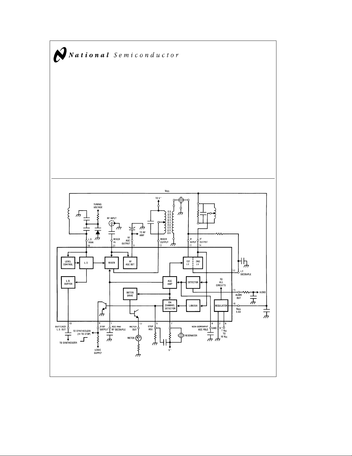
Block Diagram
May 1989
and sufficient gain are provided to allow the IC to also be
used in conjunction with a loopstick antenna.
Features
Y
Low supply current
Y
Level-controlled, low phase noise local oscillator
Y
Buffered local oscillator output
Y
Stop circuitry with adjustable stop threshold and adjustable stop window
Y
Open collector stop output
Y
Excellent THD and stop time performance
Y
Large amount of recovered audio
Y
RF AGC with open collector output
Y
Meter output
Y
Compatible with AM stereo
LM1863 AM Radio System for Electronically Tuned Radios
Order Number LM1863M
TL/H/5185– 1
See NS Package Number M20B
C
1995 National Semiconductor Corporation RRD-B30M115/Printed in U. S. A.
TL/H/5185

Absolute Maximum Ratings
Supply Voltage 16V
Package Dissipation (Note 1) 1.7W
Storage Temperature Range
b
55§Ctoa150§C
Operating Temperature Range 0§Ctoa70§C
Soldering Information
Small Outline Package
Vapor Phase (60 sec) 215
Infrared (15 sec) 220
See AN-450 ‘‘Surface Mounting Methods and Their Effect
on Product Reliability’’ for other methods of soldering surface mount devices.
C
§
C
§
Electrical Characteristics
(Test Circuit, T
STATIC CHARACTERISTICS
Supply Current V
Pin 16, Regulator Voltage 5.6 V
Operating Voltage Range (See Note 2) 7 16 V
Pin 3 Leakage Current V
Pin 9, Low Output Voltage V
Pin 17, Output Voltage V
DYNAMIC CHARACTERISTICS: (f
Maximum Sensitivity VINFor V
20 dB Quieting Sensitivity VINfor 20 dB S/N in Audio 15 30 mV
Maximum Signal to Noise Ratio V
Total Harmonic Distortion V
Total Harmonic Distortion V
Audio Output Level V
Overload Distortion V
Meter Output Voltage V
Meter Output Voltage V
Local Oscillator Output Level (See Note 3), SW1ePosition 1
on Pin 19
Local Oscillator Output Level (See Note 3), SW1ePosition 2 125 mVrms
on Pin 19
Stop Detector Valid Station V
Frequency Window the two frequencies at which 2.5 4 5.5 kHz
Stop Detector Valid Station Find VINfor which Pin 9l1V,
Signal Level Threshold SW2
RF AGC Threshold Find VINthat produces
Pin 3 Low Output Level V
Pin 9 Leakage Current V
Pin 17 Output Resistance V
Note 1: Above T
Note 2: All data sheet specifications are for V
Note 3: The local oscillator level at Pin 19 is identical to the level at Pin 18 since Pin 19 is an emitter follower off of Pin 18.
e
25§C, Vae12V, SW1ePosition 1, SW2ePosition 2, unless indicated otherwise)
A
Parameter Conditions Min Typ Max Units
e
0 mV 8.3 12.5 mA
IN
e
0 mV 0.1 mA
IN
e
0 mV, SW2ePosition 1 .15 V
IN
e
0mV 0 V
IN
MOD
e
IN
IN
IN
IN
IN
IN
IN
1 kHz, f
e
e
e
e
e
e
e
e
1 MHz, Me0.3)
IN
e
6 mVrms 7.5 mV
AUDIO
10 mV 40 54 dB
10 mV .26 %
10 mV, Me0.8 .63 2 %
10 mV 80 120 160 mVrms
50 mV, Me0.8 7.5 %
100 mV 0.5 V
10 mV 4.6 V
100 147 mVrms
e
10 mV, difference between
IN
k
Pin 9
1V, SW2ePosition 1
81670mVrms
3 6 10 mVrms
e
25§C derate based on T
A
e
Position 1
10 mA of current into Pin 3
e
30 mV 0.1 V
IN
e
30 mV 0.1 mA
IN
e
10 mV 825 X
IN
e
150§C and i
j (MAX)
ae
12V and may change slightly with supply.
e
85§C/W.
jA
2
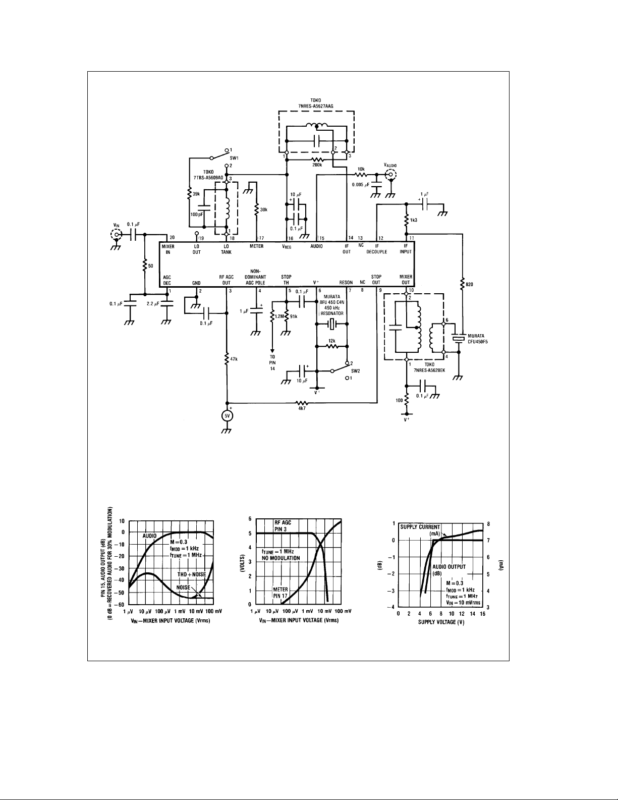
Test Circuit
Typical Performance Characteristics (From Test Circuit)
TL/H/5185– 9 TL/H/5185– 10 TL/H/5185– 11
3
TL/H/5185– 2
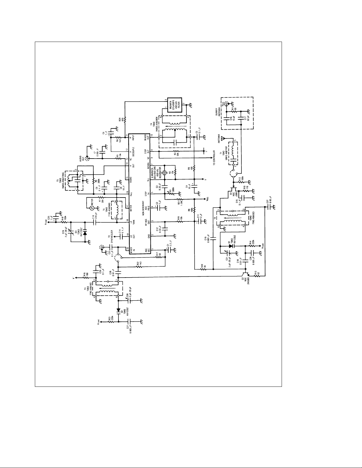
Application Circuit
TL/H/5185– 8
LM1863: AM ETR Radio
4
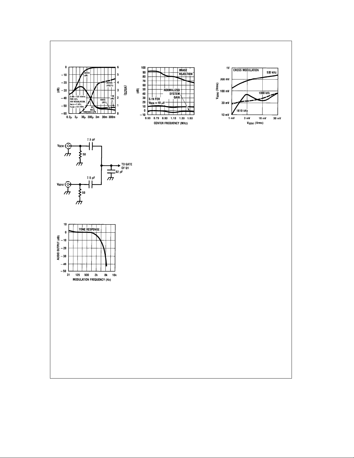
Performance Characteristics of Applications Circuit
TL/H/5185– 12
TL/H/5185– 13
TL/H/5185– 14
Cross modulation is
measured using the
following dummy antenna:
TL/H/5185– 15
TL/H/5185– 16
The following procedure was used to measure cross modulation:
1. Tune the radio to the center frequency of interest and tune V
2. Set at 0 dB audio reference with V
3. Remove the modulation from V
4. Set the modulation level of V
center frequency.
5. Increase the level of V
modulation measurement.
GEN2
,e10 mV RMS and 30% AM mod; f
GEN
and set the level of V
GEN1
GEN2
e
80% at f
MOD
e
1 kHz and tune V
untilb40 dB of audio is recovered. The level of V
, to this same frequency.
GEN
.
GEN1
GEN2
e
1 kHz.
MOD
g
40 kHz away from
is the cross
GEN2
Additional Performance Information:
* THD for 80% modulation for f
e
V
1V is 0.5%
GEN
e
V
10 mV is 0.4%
GEN
k
* Tweet
2% at all input levels.
* Typical time for valid stop indication
Note: Tweet is an audio tone produced by the 2nd and 3rd harmonic of the IF beating against the received
signal. It is measured as an equivalent modulation level: ie, 30% tweet has the same amplitude at the
detector as a desired signal with 30% modulation.
MOD
e
1 kHZ at:
k
50 ms.
5
 Loading...