

NSC LM18298T Datasheet
LM18298 Dual Full-Bridge Driver
LM18298 Dual Full-Bridge Driver
April 1992
General Description
The LM18298 is a high voltage, high current dual full-bridge
driver designed to accept standard TTL logic levels and
drive inductive loads such as relays, solenoids, DC and
stepping motors. Two enable inputs are provided to gate the
input control signals.
The emitters of the lower transistors of each bridge are connected together and the corresponding external terminal
can be used for the connection of a current sensing resistor.
An additional supply input is provided to accommodate conventional logic supply voltages.
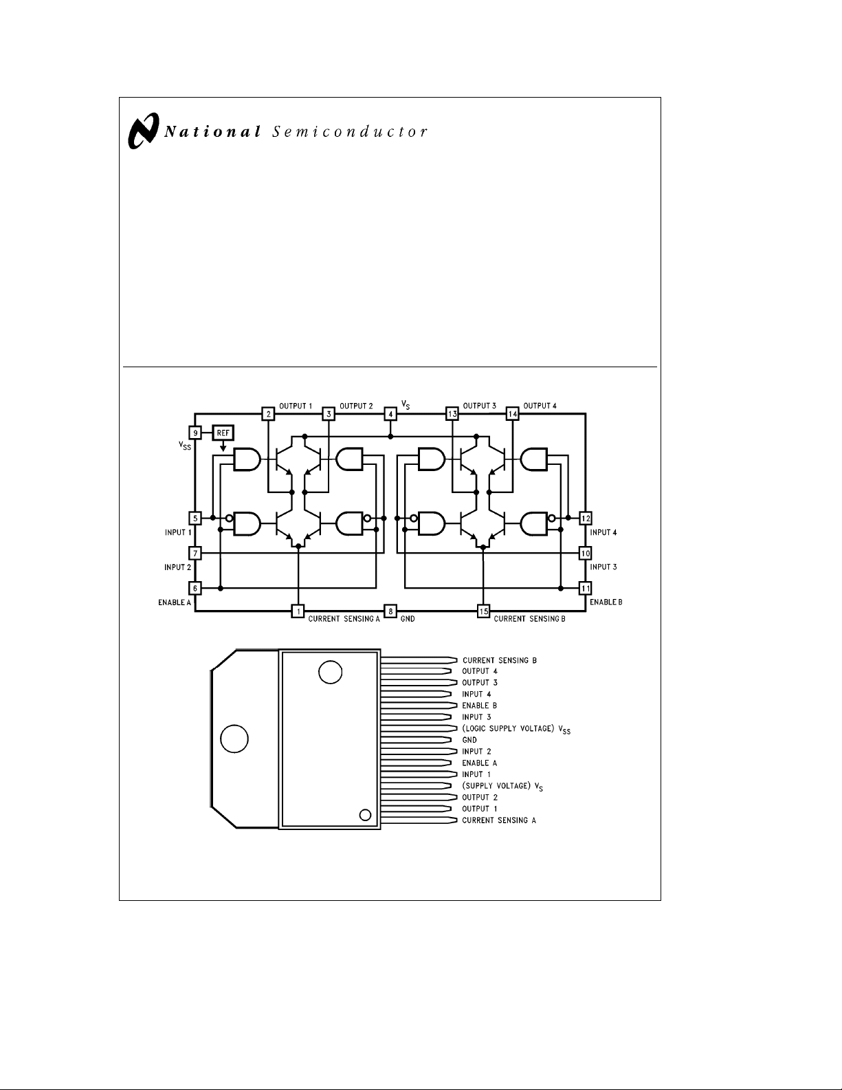
Block & Connection Diagrams
Features
Y
Power supply voltage up to 46V
Y
2A output per channel
Y
Low saturation voltage
Y
Thermal shutdown protection
Y
Logical ‘‘0’’ input voltage up to 1.5V
(High noise immunity)
Y
Pin for pin replacement for L298N
Applications
Y
DC and stepper motor drivers
Y
Relay and solenoid drivers
TL/H/9302– 1
TL/H/9302– 2
TO 220-15
Order Number LM18298T
NS Package Number TA15A
C
1995 National Semiconductor Corporation RRD-B30M115/Printed in U. S. A.
TL/H/9302
Absolute Maximum Ratings (Note 1)
If Military/Aerospace specified devices are required,
please contact the National Semiconductor Sales
Office/Distributors for availability and specifications.
Main Supply (Pin 4) 50V
Logic Supply (Pin 9) 7V
Logic Inputs
(Pins 5, 6, 7, 10, 11, 12)
Peak Output Current (Per Channel)
Non-Repetitive (t
Repetitive (80% duty cycle, t
DC Operation 2A
Electrical Characteristics
e
V
42V, V
S
e
100 ms) 3A
e
5V, I
SS
O
e
10 ms) 2.5A
ON
e
0A, T
e
J
b
0.3 to 7V
25§C, Le0V, He5V, unless otherwise specified
Symbol Parameter Conditions
V
S
V
SS
I
S
Main Supply Voltage (Pin 4) V
Logic Supply Voltage (Pin 9) 4.5 V (min)
Main Supply Quiescent Current EnableeH, InputeL9 22
(Pin 4)
EnableeH, InputeH 32 70 mA (max)
EnableeL, InputeX4
I
SS
Logic Supply Quiescent Current EnableeH, InputeL22 36
(Pin 9)
EnableeH, InputeH 6 12 mA (max)
EnableeL, InputeX6
V
IL
V
IH
I
IL
I
IH
V
EN L
V
EN H
I
EN L
I
EN H
Low Level Input Voltage
(Pins 5, 7, 10, 12)
High Level Input Voltage 2.3 V (min)
(Pins 5, 7, 10, 12)
Low Level Input Current InputeL
(Pins 5, 7, 10, 12)
High Level Input Current InputeH 30 100
(Pins 5, 7, 10, 12)
Low Level Enable Voltage
(Pins 6, 11)
High Level Enable Voltage 2.3 V (min)
(Pins 6, 11)
Low Level Enable Input Current EnableeL
(Pins 6, 11)
High Level Enable Input Current EnableeH
(Pins 6, 11)
Sense Voltage (Pins 1, 15)
Power Dissipation (Note 2) 25W
ESD Susceptibility (Note 3) 1 kV
Lead Temperature (Soldering, 10 seconds) 260§C
Storage Temperature Range
Operating Ratings
Junction Temperature Range (TJ)
Main Supply (Pin 4) 46V
b
1toa2.3V
b
65§Ctoa150§C
b
40§Ctoa150§C
Typical Limit Units
(Note 4) (Note 5) (Limits)
a
2.5 V (min)
SS
46 V (max)
7 V (max)
b
0.3 V (min)
1.5 V (max)
V
SS
b
10 mA (max)
V (max)
mA (max)
b
0.3 V (min)
1.5 V (max)
V
SS
b
10 mA (max)
V (max)
30 100 mA (max)
2

Electrical Characteristics (Continued)
e
V
S
Symbol Parameter Conditions
V
CE sat (H)
V
CE sat (L)
V
CE sat
V
sense
42V, V
e
SS
5V, I
e
O
0A, T
e
25§C, unless otherwise specified
J
Source Saturation Voltage I
(Pins 2, 3, 13, 14)
Sink Saturation Voltage I
(Pins 2, 3, 13, 14)
Total Drop I
CE sat (H)
a
V
CE sat (L)
V
Sensing Voltage (Pins 1, 15) ts50 ms
Typical Limit Units
(Note 4) (Note 5) (Limits)
e
1A 1.35 1.7
O
e
I
2A 2.0 2.7
O
e
1A 1.2 1.6
O
e
I
2A 1.7 2.3
O
e
1A 3.2
O
e
I
2A 4.9
O
Continuous
V (max)
V (max)
V (max)
b
1
b
0.5
V (min)
Continuous 2 V (max)
T
1
T
2
T
3
T
4
T
5
T
6
T
7
T
8
f
C
Note 1: Absolute Maximum Ratings indicate limits beyond which damage to the device may occur. DC and AC electrical specifications do not apply when
operating the device beyond its specified Operating Ratings.
Note 2: The maximum power dissipation must be derated at elevated temperatures and is a function of T
dissipation at any temperature is P
case thermal resistance (i
Note 3: Human body model, 100 pF discharged through a 1.5 kX resistor.
Note 4: Typicals are at 25
Note 5: Limits are guaranteed and 100% tested.
Source Current Turn-Off Delay 0.5 Input to 0.9 IO(
Source Current Fall Time 0.9 IOto 0.1 IO(
Figure 2
Source Current Turn-On Delay 0.5 Input to 0.1 IO(
Source Current Rise Time 0.1 IOto 0.9 IO(
Figure 2
Sink Current Turn-Off Delay 0.5 Input to 0.9 IO(
Sink Current Fall Time 0.9 IOto 0.1 IO(
Figure 3
Sink Current Turn-On Delay 0.5 Input to 0.1 IO(
Sink Current Rise Time 0.1 IOto 0.9 IO(
Commutation Frequency I
e
b
(T
D max
) of the LM18298 is 3§C/W.
JC
C and represent the most likely parametric norm.
§
TC)/iJCor the number given in the Absolute Maximum Ratings, whichever is lower. The typical junction-to-
J max
e
2A 25 kHz
O
Figure 3
Figure 2
) 0.5 ms
) 0.15 ms
Figure 2
) 1.3 ms
) 0.85 ms
Figure 3
) 0.25 ms
) 0.1 ms
Figure 3
) 1.3 ms
) 0.1 ms
, iJC, and TC. The maximum allowable power
J max
3
 Loading...