NSC JM38510-01204BC, JM38510-01204BD Datasheet

TL/F/6610
9601/DM9601 Retriggerable One Shot
June 1989
9601/DM9601 Retriggerable One Shot
General Description
These retriggerable one shots provide the designer with
four inputs; two active high and two active low. This permits
a choice of either leading-edge or trailing-edge triggering,
independent of input transition times. When input conditons
for triggering are met, a new cycle starts and the external
capacitor is rapidly discharged and then allowed to charge
again. The retriggerable feature allows for output pulse
widths to be expanded. In fact a continuous true output can
be maintained by having an input cycle time which is shorter
than the output cycle time. Retriggering may be inhibited by
tying the Q
output to an active low input.
Features
Y
High speed operationÐinput repetition ratel10 MHz
Y
Flexibility of operationÐoptional retriggering/lock-out
capability
Y
Output pulse width rangeÐ50 ns to
%
Y
Leading or trailing edge triggering
Y
Complementary outputs/inputs
Y
Input clamping diodes
Y
DTL/TTL compatible logic levels
Y
Alternate Military/Aerospace device (9601) is available.
Contact a National Semiconductor Sales Office/Distributor for specifications.
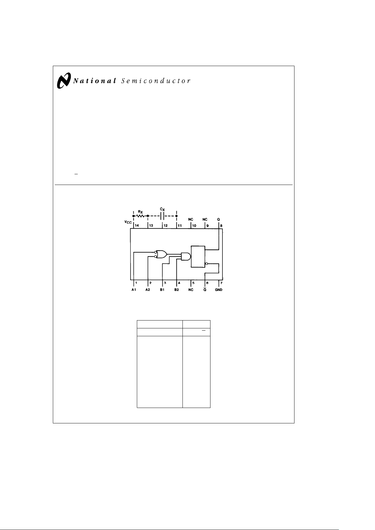
Connection Diagram
Dual-In-Line Package
TL/F/6610– 1
Order Number 9601DMQB, 9601FMQB, DM9601J, DM9601W or DM9601N
See NS Package Number J14A, N14A or W14B
Function Table
Inputs Outputs
A1 A2 B1 B2 Q Q
HeHigh Logic Level
HHXX L H
LeLow Logic Level
XXLX L H
XeEither Low or
XXXL L H
High Logic Level
LXHH L H
u
e
Low to High Level
Transition
LX
u
HÉß
v
e
High to Low Level
LXH
u
Éß
Transition
XLHH L H
ÉePositive Pulse
XL
u
HÉß
ßeNegative Pulse
XLH
u
Éß
H
v
HHÉß
vv
HHÉß
v
HHHÉß
C
1995 National Semiconductor Corporation RRD-B30M105/Printed in U. S. A.

Absolute Maximum Ratings (Note)
If Military/Aerospace specified devices are required,
please contact the National Semiconductor Sales
Office/Distributors for availability and specifications.
Supply Voltage 7V
Input Voltage 5.5V
Operating Free Air Temperature Range
Military
b
55§Ctoa125§C
Commercial 0
§
toa70§C
Storage Temperature Range
b
65§Ctoa150§C
Note:
The ‘‘Absolute Maximum Ratings’’ are those values
beyond which the safety of the device cannot be guaranteed. The device should not be operated at these limits. The
parametric values defined in the ‘‘Electrical Characteristics’’
table are not guaranteed at the absolute maximum ratings.
The ‘‘Recommended Operating Conditions’’ table will define
the conditions for actual device operation.
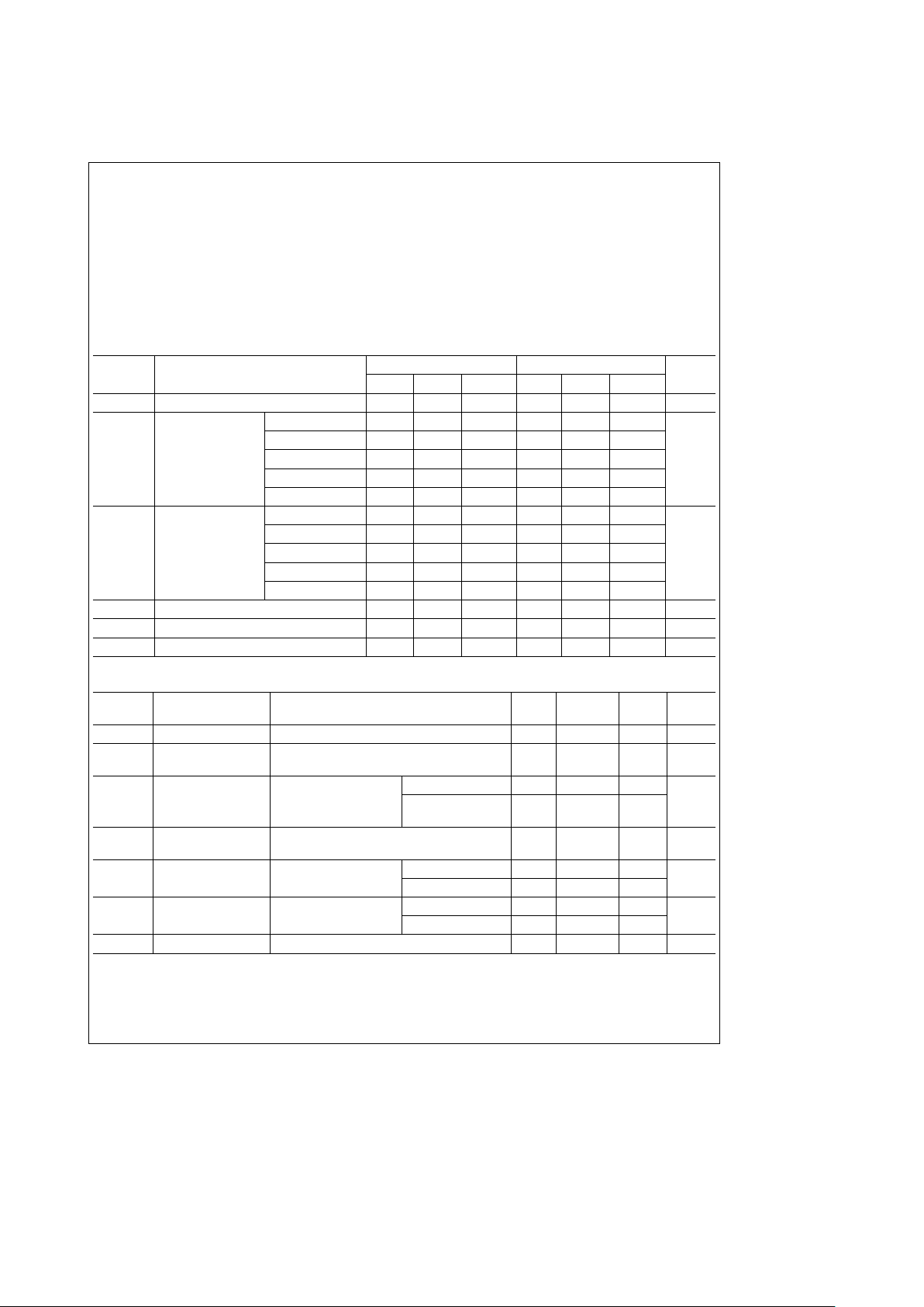
Recommended Operating Conditions
Symbol Parameter
Military Commercial
Units
Min Nom Max Min Nom Max
V
CC
Supply Voltage 4.5 5 5.5 4.75 5 5.25 V
V
IH
High Level Input T
A
eb
55§C2
Voltage
T
A
e
0§C 1.9
T
A
e
25§C 1.7 1.8 V
T
A
e
75§C 1.6
T
A
e
125§C 1.5
V
IL
Low Level Input T
A
eb
55§C 0.85
Voltage
T
A
e
0§C 0.85
T
A
e
25§C 0.9 0.85 V
T
A
e
75§C 0.85
T
A
e
125§C 0.85
I
OH
High Level Output Current
b
0.72
b
0.96 mA
I
OL
Low Level Output Current 10 12.8 mA
T
A
Free Air Operating Temperature
b
55 125 0 75
§
C
Electrical Characteristics over recommended operating free air temperature range (unless otherwise noted)
Symbol Parameter Conditions (Note 3) Min
Typ
Max Units
(Note 1)
V
I
Input Clamp Voltage V
CC
e
Min, I
I
eb
12 mA
b
1.5 V
V
OH
High Level Output V
CC
e
Min, I
OH
e
Max
2.4 V
Voltage V
IL
e
Max, V
IH
e
Min, (Note 4)
V
OL
Low Level Output V
CC
e
Min, I
OL
e
Max MIL 0.4
Voltage V
IL
e
Max, V
IH
e
Min
COM 0.45
V
(Note 4)
I
IH
High Level Input V
CC
e
Max, V
I
e
4.5V
60 mA
Current
I
IL
Low Level Input V
CC
e
Max MIL V
IN
e
0.40V
b
1.6
mA
Current
COM V
IN
e
0.45V
b
1.6
I
OS
Short Circuit V
CC
e
Max MIL
b
10
b
40
mA
Output Current (Notes 2 and 4)
COM
b
10
b
40
I
CC
Supply Current V
CC
e
Max 25 mA
Note 1: All typicals are at V
CC
e
5V, T
A
e
25§C.
Note 2: Not more than one output should be shorted at a time.
Note 3: Unless otherwise noted, R
X
e
10k between PIN 13 and VCCon all tests.
Note 4: Ground PIN 11 for V
OL
test on PIN 6, VOHand IOStests on PIN 8. Open PIN 11 for VOLtest on PIN 8, VOHand IOStests on PIN 6.
2
 Loading...