DS96172/DS96174
RS-485/RS-422 Quad Differential Line Drivers
DS96172/DS96174 RS-485/RS-422 Quad Differential Line Drivers
June 1998
General Description
The DS96172 and DS96174 are high speed quad differential
line drivers designed to meet EIA Standard RS-485. The devices have TRI-STATE
anced multipoint data bus transmission at rates up to
10 Mbps. The drivers have wide positive and negative common mode range for multipoint applications in noisy environments. Positive and negative current-limiting is provided
which protects the drivers from line fault conditions over a
+12V to −7.0V common mode range. A thermal shutdown
feature is also provided and occurs at junction temperature
of approximately 160˚C. The DS96172 features an active
high and active low Enable, common to all four drivers. The
DS96174 features separate active high Enables for each
driver pair. Compatible RS-485 receivers, transceivers, and
repeaters are also offered to provide optimum bus performance. The respective device types are DS96173,
DS96175, DS96176 AND DS96177.
®
outputs and are optimized for bal-
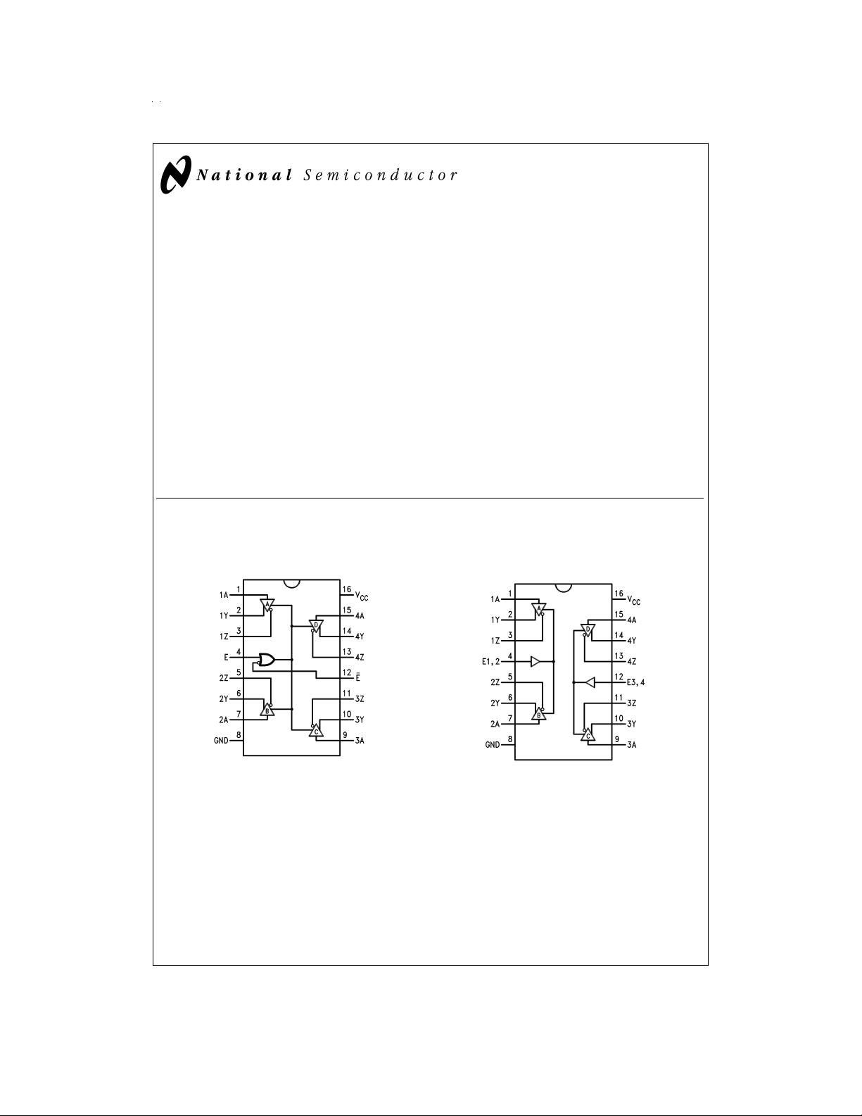
Connection Diagrams
16-Lead DIP
DS96172
Features
n Meets EIA Standard RS-485 and RS-422A
n Monotonic differential output switching
n Transmission rate to 10 Mbs
n TRI-STATE outputs
n Designed for multipoint bus transmission
n Common mode output voltage range: −7V to +12V
n Operates from single +5V supply
n Thermal shutdown protection
n DS96172/DS96174 are lead and function compatible
with the SN75172/75174 or the AM26LS31/MC3487
respectively
16-Lead DIP
DS96174
DS009626-1
Top View
Order Number DS96172CN or DS96174CN
See NS Package Number N16E
TRI-STATE®is a registered trademark of National Semiconductor Corporation.
© 1998 National Semiconductor Corporation DS009626 www.national.com
Top View
DS009626-2

Absolute Maximum Ratings (Note 2)
If Military/Aerospace specified devices are required,
please contact the National Semiconductor Sales Office/
Distributors for availability and specifications.
Storage Temperature Range
Molded DIP −65˚C to +150˚C
Operating Temperature Range 0˚C to +70˚C
Lead Temperature
Molded DIP (soldering, 10
sec.) 265˚C
Supply Voltage 7V
Enable Input Voltage 5.5V
Maximum Power Dissipation
(Note 1) 25˚C
N-Molded Package 1.98W
Recommended Operating
Conditions
Supply Voltage (V
) 4.75 5 5.25 V
CC
Common Mode Output
Voltage (V
Output Current HIGH (I
Output Current LOW (I
) −7 +12 V
OC
OH
OL
Operating Temperature (T
Note 1: Derate molded DIP package 16mW/˚C above 25˚C.
Min Typ Max Units
) −60 mA
)60mA
) 0 25 70 ˚C
A
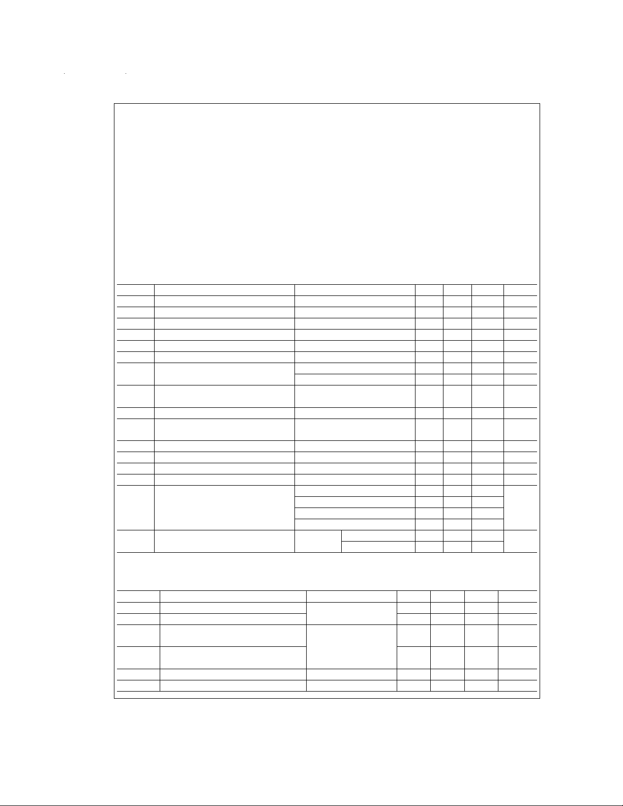
Electrical Characteristics (Notes 3, 4)
over recommended temperature and supply voltage ranges, unless otherwise specified
Symbol Parameter Conditions Min Typ Max Units
V
V
V
V
V
|V
|V
∆|V
V
∆|V
I
O
I
OZ
I
IH
I
IL
I
OS
I
CC
IH
IL
OH
OL
IC
OD1
OD2
OC
Input Voltage HIGH 2 V
Input Voltage LOW 0.8 V
Output Voltage HIGH IOH= −20 mA 3.1 V
Output Voltage LOW IOL=20mA 0.8 V
Input Clamp Voltage II= −18 mA −1.5 V
| Differential Output Voltage IO=0mA 6 V
| Differential Output Voltage RL=54Ω,
R
| Change in Magnitude of Differential RL=54Ωor 100Ω,
OD
= 100Ω,
L
Figure 1
Figure 1
Figure 1
1.5 2 V
2 2.3 V
±
0.2 V
Output Voltage (Note 5)
Common Mode Output Voltage (Note 6) RL=54Ω,
| Change in Magnitude of Common Mode
OC
Figure 1
3V
±
0.2 V
Output Voltage (Note 5)
Output Current with Power Off VCC= 0V, VO= −7.0V to 12V
High Impedance State Output Current VO= −7.0V to 12V
±
100 µA
±
50±200 µA
Input Current HIGH VI= 2.7V 20 µA
Input Current LOW VI= 0.5V −100 µA
Short Circuit Output Current VO= −7.0V −250
(Note 7) V
= 0V −150 mA
O
V
O=VCC
V
= 12V 250
O
150
Supply Current (All Drivers) No Load Outputs Enabled 50 70 mA
Output Disabled 50 60
Switching Characteristics
VCC= 5V, TA= 25˚C
Symbol Parameter Conditions Min Typ Max Units
t
DD
t
TD
t
PLH
Differential Output Delay Time RL=60Ω,
Differential Output Transition Time 15 25 ns
Propagation Delay Time, RL=27Ω,
Low-to-High Level Output
t
PHL
Propagation Delay Time, 12 20 ns
High-to-Low Level Output
t
PZH
t
PZL
www.national.com 2
Output Enable Time to High Level RL= 110Ω,
Output Enable Time to Low Level RL= 110Ω,
Figure 2
Figure 3
Figure 4
Figure 5
15 25 ns
12 20 ns
30 45 ns
30 45 ns
 Loading...