

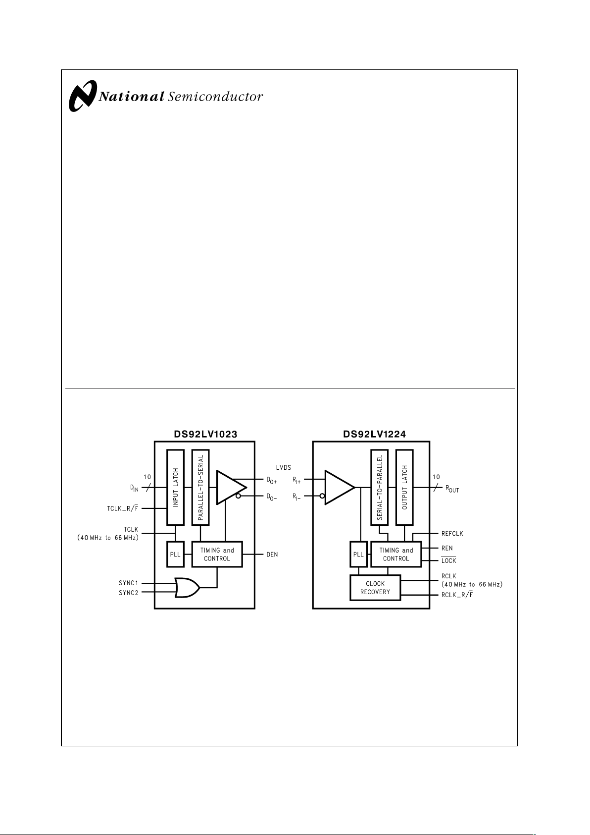
DS92LV1023 and DS92LV1224
40-66 MHz 10 Bit Bus LVDS Serializer and Deserializer
General Description
The DS92LV1023 transforms a 10-bit wide parallel
LVCMOS/LVTTL data bus into a single high speed Bus
LVDS serial data stream with embedded clock. The
DS92LV1224 receives the Bus LVDS serial data stream and
transforms it back into a 10-bit wide parallel data bus and
recovers parallel clock. The DS92LV1023 transmits data
over backplanes or cable. The single differential pair data
path makes PCB design easier. In addition, the reduced
cable, PCB trace count, and connector size tremendously
reduce cost. Since one output transmits clock and data bits
serially, it eliminates clock-to-data and data-to-data skew.
The powerdown pin saves power by reducing supply current
when not using either device. Upon power up of the Serializer, you can choose to activate synchronization mode or
allow the Deserializer to use the
synchronization-to-random-data feature. By using the synchronization mode, the Deserializer will establish lock to a
signal within specified lock times. In addition, the embedded
clock guarantees a transition on the bus every 12-bit cycle.
This eliminates transmission errors due to charged cable
conditions. Furthermore, you may put the DS92LV1023 output pins into TRI-STATE
®
to achieve a high impedance
state. The PLL can lock to frequencies between 40 MHz and
66 MHz.
Features
n Clock recovery from PLL lock to random data patterns.
n Guaranteed transition every data transfer cycle
n Chipset (Tx + Rx) power consumption
<
500 mW (typ)
@
66 MHz
n Single differential pair eliminates multi-channel skew
n Flow-through pinout for easy PCB layout
n 660 Mbps serial Bus LVDS data rate (at 66 MHz clock)
n 10-bit parallel interface for 1 byte data plus 2 control bits
n Synchronization mode and LOCK indicator
n Programmable edge trigger on clock
n High impedance on receiver inputs when power is off
n Bus LVDS serial output rated for 27Ω load
n Small 28-lead SSOP package
Block Diagrams
10093301
TRI-STATE®is a registered trademark of National Semiconductor Corporation.
June 2002
DS92LV1023 and DS92LV1224 40-66 MHz 10 Bit Bus LVDS Serializer and Deserializer
© 2002 National Semiconductor Corporation DS100933 www.national.com
Block Diagrams (Continued)
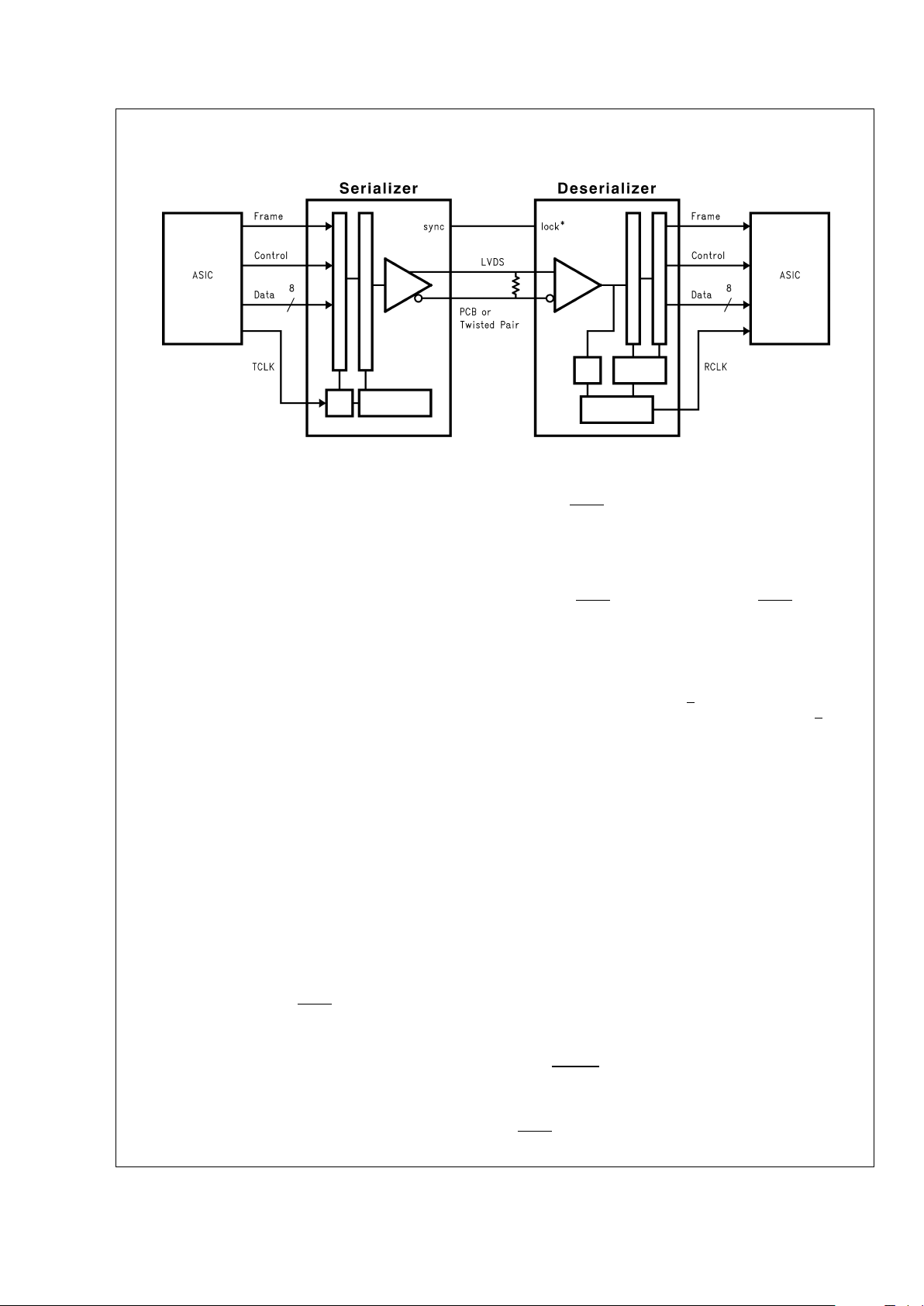
Application
10093302
Functional Description
The DS92LV1023 and DS92LV1224 are a 10-bit Serializer
and Deserializer chipset designed to transmit data over differential backplanes at clock speeds from 40 to 66 MHz. The
chipset is also capable of driving data over Unshielded
Twisted Pair (UTP) cable.
The chipset has three active states of operation: Initialization, Data Transfer, and Resynchronization; and two passive
states: Powerdown and TRI-STATE
®
.
The following sections describe each operation and passive
state.
Initialization
Initialization of both devices must occur before data transmission begins. Initialization refers to synchronization of the
Serializer and Deserializer PLL’s to local clocks, which may
be the same or separate. Afterwards, synchronization of the
Deserializer to Serializer occurs.
Step 1: When you apply V
CC
to both Serializer and/or Dese-
rializer, the respective outputs enter TRI-STATE
®
, and
on-chip power-on circuitry disables internal circuitry. When
V
CC
reaches VCCOK (2.5V) the PLL in each device begins
locking to a local clock. For the Serializer, the local clock is
the transmit clock (TCLK) provided by the source ASIC or
other device. For the Deserializer, you must apply a local
clock to the REFCLK pin.
The Serializer outputs remain in TRI-STATE while the PLL
locks to the TCLK. After locking to TCLK, the Serializer is
now ready to send data or SYNC patterns, depending on the
levels of the SYNC1 and SYNC2 inputs or a data stream.
The SYNC pattern sent by the Serializer consists of six ones
and six zeros switching at the input clock rate.
Note that the Deserializer LOCK output will remain high
while its PLL locks to the incoming data or to SYNC patterns
on the input.
Step 2: The Deserializer PLL must synchronize to the Serializer to complete initialization. The Deserializer will lock to
non-repetitive data patterns. However, the transmission of
SYNC patterns enables the Deserializer to lock to the Serializer signal within a specified time. See Figure 9.
The user’s application determines control of the SYNC1 and
SYNC 2 pins. One recommendation is a direct feedback loop
from the LOCK pin. Under all circumstances, the Serializer
stops sending SYNC patterns after both SYNC inputs return
low.
When the Deserializer detects edge transitions at the Bus
LVDS input, it will attempt to lock to the embedded clock
information. When the Deserializer locks to the Bus LVDS
clock, the LOCK output will go low. When LOCK is low, the
Deserializer outputs represent incoming Bus LVDS data.
Data Transfer
After initialization, the Serializer will accept data from inputs
DIN0–DIN9. The Serializer uses the TCLK input to latch
incoming Data. The TCLK_R/F pin selects which edge the
Serializer uses to strobe incoming data. TCLK_R/F high
selects the rising edge for clocking data and low selects the
falling edge. If either of the SYNC inputs is high for 5*TCLK
cycles, the data at DIN0-DIN9 is ignored regardless of clock
edge.
After determining which clock edge to use, a start and stop
bit, appended internally, frame the data bits in the register.
The start bit is always high and the stop bit is always low.
The start and stop bits function as the embedded clock bits
in the serial stream.
The Serializer transmits serialized data and clock bits (10+2
bits) from the serial data output (DO
±
) at 12 times the TCLK
frequency. For example, if TCLK is 66 MHz, the serial rate is
66 x 12 = 792 Mega-bits-per-second. Since only 10 bits are
from input data, the serial “payload” rate is 10 times the
TCLK frequency. For instance, if TCLK = 66 MHz, the payload data rate is 66 x 10 = 660 Mbps. The data source
provides TCLK and must be in the range of 40 MHz to 66
MHz nominal.
The Serializer outputs (DO
±
) can drive a point-to-point connection or in limited multi-point or multi-drop backplanes.
The outputs transmit data when the enable pin (DEN) is
high, PWRDN = high, and SYNC1 and SYNC2 are low.
When DEN is driven low, the Serializer output pins will enter
TRI-STATE.
When the Deserializer synchronizes to the Serializer, the
LOCK pin is low. The Deserializer locks to the embedded
DS92LV1023/DS92LV1224
www.national.com 2
Data Transfer (Continued)
clock and uses it to recover the serialized data. ROUT data
is valid when LOCK is low. Otherwise ROUT0–ROUT9 is
invalid.
The ROUT0-ROUT9 pins use the RCLK pin as the reference
to data. The polarity of the RCLK edge is controlled by the
RCLK_R/F input. See Figure 13.
ROUT(0-9), LOCK and RCLK outputs will drive a maximum
of three CMOS input gates (15 pF load) with a 66 MHz clock.
Resynchronization
When the Deserializer PLL locks to the embedded clock
edge, the Deserializer LOCK pin asserts a low. If the Deserializer loses lock, the LOCK pin output will go high and the
outputs (including RCLK) will enter TRI-STATE.
The user’s system monitors the LOCK pin to detect a loss of
synchronization. Upon detection, the system can arrange to
pulse the Serializer SYNC1 or SYNC2 pin to resynchronize.
Multiple resynchronization approaches are possible. One
recommendation is to provide a feedback loop using the
LOCK pin itself to control the sync request of the Serializer
(SYNC1 or SYNC2). Dual SYNC pins are provided for multiple control in a multi-drop application. Sending sync patterns for resynchronization is desirable when lock times
within a specific time are critical. However, the Deserializer
can lock to random data, which is discussed in the next
section.
Random Lock Initialization and
Resynchronization
The initialization and resynchronization methods described
in their respective sections are the fastest ways to establish
the link between the Serializer and Deserializer. However,
the DS92LV1224 can attain lock to a data stream without
requiring the Serializer to send special SYNC patterns. This
allows the DS92LV1224 to operate in “open-loop” applications. Equally important is the Deserializer’s ability to support
hot insertion into a running backplane. In the open loop or
hot insertion case, we assume the data stream is essentially
random. Therefore, because lock time varies due to data
stream characteristics, we cannot possibly predict exact lock
time. However, please see Table 1 for some general random
lock times under specific conditions. The primary constraint
on the “random” lock time is the initial phase relation between the incoming data and the REFCLK when the Deserializer powers up. As described in the next paragraph, the
data contained in the data stream can also affect lock time.
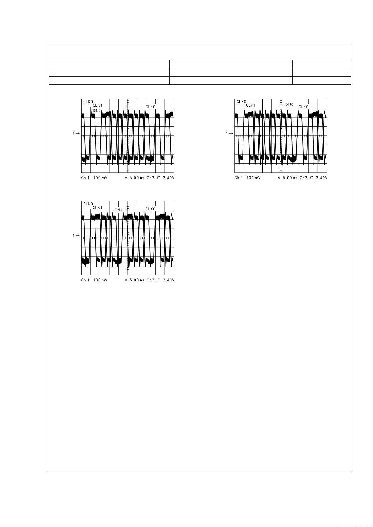
If a specific pattern is repetitive, the Deserializer could enter
“false lock” - falsely recognizing the data pattern as the
clocking bits. We refer to such a pattern as a repetitive
multi-transition, RMT. This occurs when more than one
Low-High transition takes place in a clock cycle over multiple
cycles. This occurs when any bit, except DIN 9, is held at a
low state and the adjacent bit is held high, creating a 0-1
transition. In the worst case, the Deserializer could become
locked to the data pattern rather than the clock. Circuitry
within the DS92LV1224 can detect that the possibility of
“false lock” exists. The circuitry accomplishes this by detecting more than one potential position for clocking bits. Upon
detection, the circuitry will prevent the LOCK output from
becoming active until the potential “false lock” pattern
changes. The false lock detect circuitry expects the data will
eventually change, causing the Deserializer to lose lock to
the data pattern and then continue searching for clock bits in
the serial data stream. Graphical representations of RMT are
shown in Figure 1. Please note that RMT only applies to bits
DIN0-DIN8.
Powerdown
When no data transfer occurs, you can use the Powerdown
state. The Serializer and Deserializer use the Powerdown
state, a low power sleep mode, to reduce power consumption. The Deserializer enters Powerdown when you drive
PWRDN and REN low. The Serializer enters Powerdown
when you drive PWRDN low. In Powerdown, the PLL stops
and the outputs enterTRI-STATE, which disables load current and reduces supply current to the milliampere range. To
exit Powerdown, you must drive the PWRDN pin high.
Before valid data exchanges between the Serializer and
Deserializer, you must reinitialize and resynchronize the devices to each other. Initialization of the Serializer takes 510
TCLK cycles. The Deserializer will initialize and assert LOCK
high until lock to the Bus LVDS clock occurs.
TRI-STATE
The Serializer enters TRI-STATE when the DEN pin is driven
low. This puts both driver output pins (DO+ and DO−) into
TRI-STATE. When you drive DEN high, the Serializer returns
to the previous state, as long as all other control pins remain
static (SYNC1, SYNC2, PWRDN, TCLK_R/F).
When you drive the REN pin low, the Deserializer enters
TRI-STATE. Consequently, the receiver output pins
(ROUT0–ROUT9) and RCLK will enter TRI-STATE. The
LOCK output remains active, reflecting the state of the PLL.
TABLE 1.
Random Lock Times for the DS92LV1224
40 MHz 66 MHz Units
Maximum 26 18 µS
Mean 4.5 3.0 µS
Minimum 0.77 0.43 µS
Conditions: PRBS 2
15
,VCC= 3.3V
1) Difference in lock times are due to different starting points in the data
pattern with multiple parts.
DS92LV1023/DS92LV1224
www.national.com3
Ordering Information
NSID Function Package
DS92LV1023TMSA Serializer MSA28
DS92LV1224TMSA Deserializer MSA28
10093324
DIN0 Held Low-DIN1 Held High Creates an RMT Pattern
10093325
DIN4 Held Low-DIN5 Held High Creates an RMT Pattern
10093326
DIN8 Held Low-DIN9 Held High Creates an RMT Pattern
FIGURE 1. RMT Patterns Seen on the Bus LVDS Serial Output
DS92LV1023/DS92LV1224
www.national.com 4
Absolute Maximum Ratings (Note 1)
If Military/Aerospace specified devices are required,
please contact the National Semiconductor Sales Office/
Distributors for availability and specifications.
Supply Voltage (V
CC
) −0.3V to +4V
LVCMOS/LVTTL Input
Voltage −0.3V to (V
CC
+0.3V)
LVCMOS/LVTTL Output
Voltage −0.3V to (VCC+0.3V)
Bus LVDS Receiver Input
Voltage −0.3V to +3.9V
Bus LVDS Driver Output
Voltage −0.3V to +3.9V
Bus LVDS Output Short
Circuit Duration 10mS
Junction Temperature +150˚C
Storage Temperature −65˚C to +150˚C
Lead Temperature
(Soldering, 4 seconds) +260˚C
Maximum Package Power Dissipation Capacity
@
25˚C Package:
28L SSOP 1.27 W
Package Derating:
28L SSOP
10.3 mW/˚C above
+25˚C
θ
ja
97˚C/W
θ
jc
27˚C/W
ESD Rating for
DS92LV1023
HBM (1.5kOhm, 100pF)
>
1kV
MM
>
250V
ESD Rating for
DS92LV1224
HBM (1.5kOhm, 100pF)
>
2kV
MM
>
250V
Recommended Operating
Conditions
Min Nom Max Units
Supply Voltage (V
CC
) 3.0 3.3 3.6 V
Operating Free Air
Temperature (T
A
)
−40 +25 +85 ˚C
Receiver Input Range 0 2.4 V
Supply Noise Voltage
(V
CC
)
100 mV
P-P
Electrical Characteristics
Over recommended operating supply and temperature ranges unless otherwise specified.
Symbol Parameter Conditions Min Typ Max Units
SERIALIZER LVCMOS/LVTTL DC SPECIFICATIONS (apply to DIN0-9, TCLK, PWRDN, TCLK_R/F, SYNC1, SYNC2, DEN)
V
IH
High Level Input Voltage 2.0 V
CC
V
V
IL
Low Level Input Voltage GND 0.8 V
V
CL
Input Clamp Voltage ICL= −18 mA -0.86 −1.5 V
I
IN
Input Current VIN= 0V or 3.6V −10
±
1 +10 µA
DESERIALIZER LVCMOS/LVTTL DC SPECIFICATIONS (apply to pins PWRDN, RCLK_R/ F, REN, REFCLK = inputs; apply
to pins ROUT, RCLK, LOCK = outputs)
V
IH
High Level Input Voltage 2.0 V
CC
V
V
IL
Low Level Input Voltage GND 0.8 V
V
CL
Input Clamp Voltage ICL= −18 mA −0.62 −1.5 V
I
IN
Input Current VIN= 0V or 3.6V −10
±
1 +15 µA
V
OH
High Level Output Voltage IOH= −9 mA 2.2 3.0 V
CC
V
V
OL
Low Level Output Voltage IOL= 9 mA GND 0.25 0.5 V
I
OS
Output Short Circuit Current VOUT = 0V −15 −47 −85 mA
I
OZ
TRI-STATE Output Current PWRDN or REN = 0.8V, V
OUT
=0VorVCC −10
±
0.1 +10 µA
SERIALIZER Bus LVDS DC SPECIFICATIONS (apply to pins DO+ and DO−)
V
OD
Output Differential Voltage
(DO+)–(DO−)
RL=27Ω, Figure 18
200 290 mV
∆V
OD
Output Differential Voltage
Unbalance
35 mV
V
OS
Offset Voltage 1.05 1.1 1.3 V
∆V
OS
Offset Voltage Unbalance 4.8 35 mV
DS92LV1023/DS92LV1224
www.national.com5
Electrical Characteristics (Continued)
Over recommended operating supply and temperature ranges unless otherwise specified.
Symbol Parameter Conditions Min Typ Max Units
I
OS
Output Short Circuit Current D0 = 0V, DIN = High,PWRDN and DEN =
2.4V
−56 −90 mA
I
OZ
TRI-STATE Output Current PWRDN or DEN = 0.8V, DO = 0V or VCC −10
±
1 +10 µA
I
OX
Power-Off Output Current VCC = 0V, DO=0V or 3.6V −20
±
1 +25 µA
DESERIALIZER Bus LVDS DC SPECIFICATIONS (apply to pins RI+ and RI−)
VTH Differential Threshold High Voltage VCM = +1.1V +6 +50 mV
VTL Differential Threshold Low Voltage −50 −12 mV
I
IN
Input Current VIN= +2.4V, VCC= 3.6V or 0V −10
±
1 +15 µA
V
IN
= 0V, VCC= 3.6V or 0V −10±0.05 +10 µA
SERIALIZER SUPPLY CURRENT (apply to pins DVCC and AVCC)
I
CCD
Serializer Supply Current RL = 27Ω f = 40 MHz 47 60 mA
Worst Case Figure 2 f = 66 MHz 75 90 mA
I
CCXD
Serializer Supply Current Powerdown PWRDN = 0.8V 47 500 µA
DESERIALIZER SUPPLY CURRENT (apply to pins DVCC and AVCC)
I
CCR
Deserializer Supply Current CL= 15 pF f = 40 MHz 58 75 mA
Worst Case Figure 3 f = 66 MHz 90 110 mA
I
CCXR
Deserializer Supply Current
Powerdown
PWRDN = 0.8V, REN = 0.8V
0.36 1.0 mA
Serializer Timing Requirements for TCLK
Over recommended operating supply and temperature ranges unless otherwise specified.
Symbol Parameter Conditions Min Typ Max Units
t
TCP
Transmit Clock Period 15.15 T 25.0 nS
t
TCIH
Transmit Clock High Time 0.4T 0.5T 0.6T nS
t
TCIL
Transmit Clock Low Time 0.4T 0.5T 0.6T nS
t
CLKT
TCLK Input Transition
Time
36nS
t
JIT
TCLK Input Jitter
Figure 17 150
pS
(RMS)
Serializer Switching Characteristics
Over recommended operating supply and temperature ranges unless otherwise specified.
Symbol Parameter Conditions Min Typ Max Units
t
LLHT
Bus LVDS Low-to-High
Transition Time
RL=27Ω
C
L
=10pF to GND
Figure 4
(Note 4)
0.2 0.4 nS
t
LHLT
Bus LVDS High-to-Low
Transition Time
0.25 0.4 nS
t
DIS
DIN (0-9) Setup to TCLK RL=27Ω,
C
L
=10pF to GND
Figure 7
0nS
t
DIH
DIN (0-9) Hold from TCLK
4.0 nS
t
HZD
DO±HIGH to
TRI-STATE Delay
RL=27Ω,
C
L
=10pF to GND
Figure 8
(Note 5)
310nS
t
LZD
DO±LOW to TRI-STATE
Delay
310nS
t
ZHD
DO±TRI-STATE to
HIGH Delay
510nS
t
ZLD
DO±TRI-STATE to LOW
Delay
6.5 10 nS
DS92LV1023/DS92LV1224
www.national.com 6

Serializer Switching Characteristics (Continued)
Over recommended operating supply and temperature ranges unless otherwise specified.
Symbol Parameter Conditions Min Typ Max Units
t
SPW
SYNC Pulse Width RL=27Ω
Figure 10
5*t
TCP
nS
t
PLD
Serializer PLL Lock Time 510*t
TCP
513*t
TCP
nS
t
SD
Serializer Delay RL=27Ω, Figure 11 t
TCP
+ 1.0 t
TCP
+ 2.0 t
TCP
+ 3.0 nS
t
DJIT
Deterministic Jitter
R
L
=27Ω,
C
L
=10pF
to GND,
(Note 6)
40
MHz
-320 -80 150 pS
66
MHz
-200 -70 80 pS
t
RJIT
Random Jitter RL=27Ω,
C
L
=10pF to GND
19 25 pS (RMS)
Deserializer Timing Requirements for REFCLK
Over recommended operating supply and temperature ranges unless otherwise specified.
Symbol Parameter Conditions Min Typ Max Units
t
RFCP
REFCLK Period 15.15 T 25 nS
t
RFDC
REFCLK Duty Cycle 30 50 70 %
t
RFCP
/
t
TCP
Ratio of REFCLK to
TCLK
95 1 105
t
RFTT
REFCLK Transition Time 3 6 nS
Deserializer Switching Characteristics
Over recommended operating supply and temperature ranges unless otherwise specified.
Symbol Parameter Conditions Pin/Freq. Min Typ Max Units
t
RCP
Receiver out Clock
Period
t
RCP=tTCP
Figure 11
RCLK 15.15 25 nS
t
CLH
CMOS/TTL
Low-to-High Transition
Time
CL=15pF
Figure 5
Rout(0-9),
LOCK,
RCLK
1.2 4 nS
t
CHL
CMOS/TTL
High-to-Low Transition
Time
1.1 4 nS
t
DD
Deserializer Delay
Figure 12
All Temp./ All
Freq.
1.75*t
RCP
+1.25 1.75*t
RCP
+3.75 1.75*t
RCP
+6.25 nS
Room Temp./
3.3V/40MHz
1.75*t
RCP
+2.25 1.75*t
RCP
+3.75 1.75*t
RCP
+5.25 nS
Room Temp./
3.3V/66MHz
1.75*t
RCP
+2.75 1.75*t
RCP
+3.75 1.75*t
RCP
+4.75 nS
t
ROS
ROUT Data Valid
before RCLK
Figure 13 RCLK
40MHz
0.4*t
RCP
0.5*t
RCP
nS
RCLK
66MHz
0.38*t
RCP
0.5*t
RCP
nS
t
ROH
ROUT Data valid after Figure 13 40MHz −0.4*t
RCP
−0.5*t
RCP
nS
RCLK 66MHz −0.38*t
RCP
−0.5*t
RCP
nS
t
RDC
RCLK Duty Cycle 45 50 55 %
DS92LV1023/DS92LV1224
www.national.com7

Deserializer Switching Characteristics (Continued)
Over recommended operating supply and temperature ranges unless otherwise specified.
Symbol Parameter Conditions Pin/Freq. Min Typ Max Units
t
HZR
HIGH to TRI-STATE
Delay
Figure 14 Rout(0-9)
2.8 10 nS
t
LZR
LOW to TRI-STATE
Delay
2.8 10 nS
t
ZHR
TRI-STATE to HIGH
Delay
4.2 10 nS
t
ZLR
TRI-STATE to LOW
Delay
4.2 10 nS
t
DSR1
Deserializer PLL Lock
Time from PWRDWN
(with SYNCPAT)
Figure 15
Figure 16
(Note 7)
40MHz 1.31 3 µS
66MHz 0.84 3 µS
t
DSR2
Deserializer PLL Lock
time from SYNCPAT
40MHz 0.47 1 µS
66MHz 0.29 0.8 µS
t
ZHLK
TRI-STATE to HIGH
Delay (power-up)
LOCK
3.7 12 nS
t
RNM
Deserializer Noise
Margin
Figure 17
(Note 8)
40 MHz 450 730 pS
66 MHz 250 400 pS
Note 1: “Absolute Maximum Ratings” are those values beyond which the
safety of the device cannot be guaranteed. They are not meant to imply that
the devices should be operated at these limits. The table of “Electrical
Characteristics” specifies conditions of device operation.
Note 2: Typical values are given for V
CC
= 3.3V and TA= +25˚C.
Note 3: Current into device pins is defined as positive. Current out of device
pins is defined as negative. Voltages are referenced to ground except VOD,
∆VOD, VTH and VTL which are differential voltages.
Note 4: t
LLHT
and t
LHLT
specifications are Guranteed By Design (GBD)
using statistical analysis.
Note 5: Because the Serializer is in TRI-STATE mode, the Deserializer will
lose PLL lock and have to resynchronize before data transfer.
Note 6: t
DJIT
specifications are Guranteed By Design using statistical analy-
sis.
Note 7: For the purpose of specifying deserializer PLL performance, tDSR1
and tDSR2 are specified with the REFCLK running and stable, and with
specific conditions for the incoming data stream (SYNCPATs). It is recommended that the derserializer be initialized using either t
DSR1
timing or t
DSR2
timing. t
DSR1
is the time required for the deserializer to indicate lock upon
power-up or when leaving the power-down mode. Synchronization patterns
should be sent to the device before initiating either condition. t
DSR2
is the time
required to indicate lock for the powered-up and enabled deserializer when
the input (RI+ and RI-) conditions change from not receiving data to receiving
synchronization patterns (SYNCPATs).
Note 8: t
RNM
is a measure of how much phase noise (jitter) the deserializer
can tolerate in the incoming data stream before bit errors occur. The Deserializer Noise Margin is Guaranteed By Design (GBD) using statistical
analysis.
AC Timing Diagrams and Test Circuits
10093303
FIGURE 2. “Worst Case” Serializer ICC Test Pattern
DS92LV1023/DS92LV1224
www.national.com 8

AC Timing Diagrams and Test Circuits (Continued)
10093304
FIGURE 3. “Worst Case” Deserializer ICC Test Pattern
10093305
FIGURE 4. Serializer Bus LVDS Output Load and Transition Times
10093306
FIGURE 5. Deserializer CMOS/TTL Output Load and Transition Times
10093307
FIGURE 6. Serializer Input Clock Transition Time
DS92LV1023/DS92LV1224
www.national.com9

AC Timing Diagrams and Test Circuits (Continued)
10093308
Timing shown for TCLK_R/F = LOW
FIGURE 7. Serializer Setup/Hold Times
10093309
FIGURE 8. Serializer TRI-STATE Test Circuit and Timing
10093310
FIGURE 9. Serializer PLL Lock Time, and PWRDN TRI-STATE Delays
DS92LV1023/DS92LV1224
www.national.com 10

AC Timing Diagrams and Test Circuits (Continued)
10093323
FIGURE 10. SYNC Timing Delays
10093311
FIGURE 11. Serializer Delay
10093312
FIGURE 12. Deserializer Delay
DS92LV1023/DS92LV1224
www.national.com11
AC Timing Diagrams and Test Circuits (Continued)
10093313
Timing shown for RCLK_R/F = LOW
Duty Cycle (t
RDC
)=
FIGURE 13. Deserializer Data Valid Out Times
10093314
FIGURE 14. Deserializer TRI-STATE Test Circuit and Timing
DS92LV1023/DS92LV1224
www.national.com 12
AC Timing Diagrams and Test Circuits (Continued)
10093315
FIGURE 15. Deserializer PLL Lock Times and PWRDN TRI-STATE Delays
10093322
FIGURE 16. Deserializer PLL Lock Time from SyncPAT
DS92LV1023/DS92LV1224
www.national.com13

AC Timing Diagrams and Test Circuits (Continued)
10093321
SW - Setup and Hold Time (Internal Data Sampling Window)
t
DJIT
- Serializer Output Bit Position Jitter that results from Jitter on TCLK
t
RNM
= Receiver Noise Margin Time
FIGURE 17. Receiver Bus LVDS Input Skew Margin
10093316
VOD= (DO+)–(DO−).
Differential output signal is shown as (DO+)– (DO−), device in Data Transfer mode.
FIGURE 18. VODDiagram
DS92LV1023/DS92LV1224
www.national.com 14

Application Information
Using the DS92LV1023 and DS92LV1224
The Serializer and Deserializer chipset is an easy to use
transmitter and receiver pair that sends 10 bits of parallel
LVTTL data over a serial Bus LVDS link up to 660 Mbps. An
on-board PLL serializes the input data and embeds two clock
bits within the data stream. The Deserializer uses a separate
reference clock (REFCLK) and an onboard PLL to extract
the clock information from the incoming data stream and
then deserialize the data. The Deserializer monitors the
incoming clock information, determines lock status, and asserts the LOCK output high when loss of lock occurs.
Power Considerations
An all CMOS design of the Serializer and Deserializer makes
them inherently low power devices. In addition, the constant
current source nature of the Bus LVDS outputs minimizes
the slope of the speed vs. I
CC
curve of conventional CMOS
designs.
Powering Up the Deserializer
The DS92LV1224 can be powered up at any time by following the proper sequence. The REFCLK input can be running
before the Deserializer powers up, and it must be running in
order for the Deserializer to lock to incoming data. The
Deserializer outputs will remain in TRI-STATE until the Deserializer detects data transmission at its inputs and locks to
the incoming data stream.
Transmitting Data
Once you power up the Serializer and Deserializer, they
must be phase locked to each other to transmit data. Phase
locking occurs when the Deserializer locks to incoming data
or when the Serializer sends patterns. The Serializer sends
SYNC patterns whenever the SYNC1 or SYNC2 inputs are
high. The LOCK output of the Deserializer remains high until
it has locked to the incoming data stream. Connecting the
LOCK output of the Deserializer to one of the SYNC inputs of
the Serializer will guarantee that enough SYNC patterns are
sent to achieve Deserializer lock.
The Deserializer can also lock to incoming data by simply
powering up the device and allowing the “random lock”
circuitry to find and lock to the data stream.
While the Deserializer LOCK output is low, data at the Deserializer outputs (ROUT0-9) is valid, except for the specific
case of loss of lock during transmission which is further
discussed in the ’Recovering from LOCK Loss’ section below.
Noise Margin
The Deserializer noise margin is the amount of input jitter
(phase noise) that the Deserializer can tolerate and still
reliably receive data. Various environmental and systematic
factors include:
Serializer: TCLK jitter, V
CC
noise (noise bandwidth and
out-of-band noise)
Media: ISI, Large V
CM
shifts
Deserializer: V
CC
noise
Recovering from LOCK Loss
In the case where the Deserializer loses lock during data
transmission, up to 3 cycles of data that were previously
received can be invalid. This is due to the delay in the lock
detection circuit. The lock detect circuit requires that invalid
clock information be received 4 times in a row to indicate
loss of lock. Since clock information has been lost, it is
possible that data was also lost during these cycles. There-
fore, after the Deserializer relocks to the incoming data
stream and the Deserializer LOCK pin goes low, at least
three previous data cycles should be suspect for bit errors.
The Deserializer can relock to the incoming data stream by
making the Serializer resend SYNC patterns, as described
above, or by random locking, which can take more time,
depending on the data patterns being received.
Hot Insertion
All the BLVDS devices are hot pluggable if you follow a few
rules. When inserting, ensure the Ground pin(s) makes contact first, then the VCC pin(s), and then the I/O pins. When
removing, the I/O pins should be unplugged first, then the
VCC, then the Ground. Random lock hot insertion is illustrated in Figure 21.
PCB Considerations
The Bus LVDS Serializer and Deserializer should be placed
as close to the edge connector as possible. In multiple
Deserializer applications, the distance from the Deserializer
to the slot connector appears as a stub to the Serializer
driving the backplane traces. Longer stubs lower the impedance of the bus, increase the load on the Serializer, and
lower the threshold margin at the Deserializers. Deserializer
devices should be placed much less than one inch from slot
connectors. Because transition times are very fast on the
Serializer Bus LVDS outputs, reducing stub lengths as much
as possible is the best method to ensure signal integrity.
Transmission Media
The Serializer and Deserializer can also be used in
point-to-point configuration of a backplane, through a PCB
trace, or through twisted pair cable. In point-to-point configuration, the transmission media need only be terminated at
the receiver end. Please note that in point-to-point configuration, the potential of offsetting the ground levels of the
Serializer vs. the Deserializer must be considered. Also, Bus
LVDS provides a +/− 1.2V common mode range at the
receiver inputs.
Failsafe Biasing for the DS92LV1224
The DS92LV1224 has an improved input threshold sensitivity of +/− 50mV versus +/− 100mV for the DS92LV1210 or
DS92LV1212. This allows for greater differential noise margin in the DS92LV1224. However, in cases where the receiver input is not being actively driven, the increased sensitivity of the DS92LV1224 can pickup noise as a signal and
cause unintentional locking . For example, this can occur
when the input cable is disconnected.
External resistors can be added to the receiver circuit board
to prevent noise pick-up. Typically, the non-inverting receiver
input is pulled up and the inverting receiver input is pulled
down by high value resistors. the pull-up and pull-down
resistors (R
1
and R2) provide a current path through the
termination resistor (R
L
) which biases the receiver inputs
when they are not connected to an active driver. The value of
the pull-up and pull-down resistors should be chosen so that
enough current is drawn to provide a +15mV drop across the
termination resistor. Please see Figure 19 for the Failsafe
Biasing Setup.
Using t
DJIT
and t
RNM
to Validate Signal Quality
The parameters t
DJIT
and t
RNM
can be used to generate an
eye pattern mask to validate signal quality in an actual
application or in simulation.
The parameter t
DJIT
measures the transmitter’s ability to
place data bits in the ideal position to be sampled by the
receiver. The typical t
DJIT
parameter of −80pS indicates that
the crossing point of the Tx data is 80pS ahead of the ideal
DS92LV1023/DS92LV1224
www.national.com15

Application Information (Continued)
crossing point. The t
DJIT(min)
and t
DJIT(max)
parameters
specify the earliest and latest, repectively, time that a crossing will occur relative to the ideal position.
The parameter t
RNM
is calculated by first measuring how
much of the ideal bit the receiver needs to ensure correct
sampling. After determining this amount, what remains of the
ideal bit that is available for external sources of noise is
called t
RNM
. It is the offset from t
DJIT(min or max)
for the test
mask within the eye opening.
The vertical limits of the mask are determined by the
DS92LV1224 receiver input threshold of +/− 50mV.
Please refer to the eye mask pattern of Figure 20 for a
graphic representation of t
DJIT
and t
RNM
.
10093327
FIGURE 19. Failsafe Biasing Setup
10093328
FIGURE 20. Using t
DJIT
and t
RNM
to Generate an Eye Pattern Mask and Validate Signal Quality
DS92LV1023/DS92LV1224
www.national.com 16

Application Information (Continued)
Pin Diagrams
DS92LV1023TMSA - Serializer
10093318
10093317
FIGURE 21. Random Lock Hot Insertion
DS92LV1023/DS92LV1224
www.national.com17

Pin Diagrams (Continued)
DS92LV1224TMSA - Deserializer
10093319
Serializer Pin Description
Pin Name I/O No. Description
DIN I 3–12 Data Input. LVTTL levels inputs. Data on these pins are loaded into
a 10-bit input register.
TCLK_R/F
I 13 Transmit Clock Rising/Falling strobe select. LVTTL level input.
Selects TCLK active edge for strobing of DIN data. High selects
rising edge. Low selects falling edge.
DO+ O 22 + Serial Data Output. Non-inverting Bus LVDS differential output.
DO− O 21 − Serial Data Output. Inverting Bus LVDS differential output.
DEN I 19 Serial Data Output Enable. LVTTL level input. A low, puts the Bus
LVDS outputs in TRI-STATE.
PWRDN
I 24 Powerdown. LVTTL level input. PWRDN driven low shuts down the
PLL and TRI-STATEs outputs putting the device into a low power
sleep mode.
TCLK I 14 Transmit Clock. LVTTL level input. Input for 40 MHz–66 MHz
(nominal) system clock.
SYNC I 1, 2 Assertion of SYNC (high) for at least 1024 synchronization symbols
to be transmitted on the Bus LVDS serial output. Synchronization
symbols continue to be sent if SYNC continues asserted. TTL level
input. The two SYNC pins are ORed.
DVCC I 27, 28 Digital Circuit power supply.
DGND I 15, 16 Digital Circuit ground.
AVCC I 17, 26 Analog power supply (PLL and Analog Circuits).
AGND I 18, 25, 20, 23 Analog ground (PLL and Analog Circuits).
Deserializer Pin Description
Pin Name I/O No. Description
ROUT O 15–19, 24–28 Data Output.
±
9 mA CMOS level outputs.
RCLK_R/F
I 2 Recovered Clock Rising/Falling strobe select. TTL level input.
Selects RCLK active edge for strobing of ROUT data. High selects
rising edge. Low selects falling edge.
RI+ I 5 + Serial Data Input. Non-inverting Bus LVDS differential input.
DS92LV1023/DS92LV1224
www.national.com 18

Deserializer Pin Description (Continued)
Pin Name I/O No. Description
RI− I 6 − Serial Data Input. Inverting Bus LVDS differential input.
PWRDN
I 7 Powerdown. TTL level input. PWRDN driven low shuts down the PLL
and TRI-STATEs outputs putting the device into a low power sleep
mode.
LOCK O 10 LOCK goes low when the Deserializer PLL locks onto the embedded
clock edge. CMOS level output. Totem pole output structure, does
not directly support wire OR connection.
RCLK O 9 Recovered Clock. Parallel data rate clock recovered from embedded
clock. Used to strobe ROUT, CMOS level output.
REN I 8 Output Enable. TTL level input. TRI-STATEs ROUT0–ROUT9, LOCK
and RCLK when driven low.
DVCC I 21, 23 Digital Circuit power supply.
DGND I 14, 20, 22 Digital Circuit ground.
AVCC I 4, 11 Analog power supply (PLL and Analog Circuits).
AGND I 1, 12, 13 Analog ground (PLL and Analog Circuits).
REFCLK I 3 Use this pin to supply a REFCLK signal for the internal PLL
frequency.
Deserializer Truth Table
INPUTS OUTPUTS
PWRDN
REN ROUT [0:9] LOCK RCLK
HHZHZ
H H Active L Active
LXZZZ
H L Z Active Z
1) LOCK Active indicates the LOCK output will reflect the state of the Deserializer with regard to the selected data stream.
2) RCLK Active indicates the RCLK will be running if the Deserializer is locked. The Timing of RCLK with respect to ROUT is determined by RCLK_R/F.
3) ROUT and RCLK are TRI-STATED when LOCK is asserted High.
DS92LV1023/DS92LV1224
www.national.com19

Physical Dimensions inches (millimeters)
unless otherwise noted
Order Number DS92LV1023TMSA or DS92LV1224TMSA
NS Package Number MSA28
LIFE SUPPORT POLICY
NATIONAL’S PRODUCTS ARE NOT AUTHORIZED FOR USE AS CRITICAL COMPONENTS IN LIFE SUPPORT
DEVICES OR SYSTEMS WITHOUT THE EXPRESS WRITTEN APPROVAL OF THE PRESIDENT AND GENERAL
COUNSEL OF NATIONAL SEMICONDUCTOR CORPORATION. As used herein:
1. Life support devices or systems are devices or
systems which, (a) are intended for surgical implant
into the body, or (b) support or sustain life, and
whose failure to perform when properly used in
accordance with instructions for use provided in the
labeling, can be reasonably expected to result in a
significant injury to the user.
2. A critical component is any component of a life
support device or system whose failure to perform
can be reasonably expected to cause the failure of
the life support device or system, or to affect its
safety or effectiveness.
National Semiconductor
Corporation
Americas
Email: support@nsc.com
National Semiconductor
Europe
Fax: +49 (0) 180-530 85 86
Email: europe.support@nsc.com
Deutsch Tel: +49 (0) 69 9508 6208
English Tel: +44 (0) 870 24 0 2171
Français Tel: +33 (0) 1 41 91 8790
National Semiconductor
Asia Pacific Customer
Response Group
Tel: 65-2544466
Fax: 65-2504466
Email: ap.support@nsc.com
National Semiconductor
Japan Ltd.
Tel: 81-3-5639-7560
Fax: 81-3-5639-7507
www.national.com
DS92LV1023 and DS92LV1224 40-66 MHz 10 Bit Bus LVDS Serializer and Deserializer
National does not assume any responsibility for use of any circuitry described, no circuit patent licenses are implied and National reserves the right at any time without notice to change said circuitry and specifications.
 Loading...