

DS75176B/DS75176BT
Multipoint RS-485/RS-422 Transceivers
General Description
The DS75176B is a high speed differential TRI-STATE
®
bus/line transceiver designed to meet the requirements of
EIA standard RS485 with extended common mode range
(+12V to −7V), for multipoint data transmission. In addition, it
is compatible with RS-422.
The driver and receiver outputs feature TRI-STATE capability, for the driver outputs over the entire common mode
range of +12V to −7V. Bus contention or fault situations that
cause excessive power dissipation within the device are
handled by a thermal shutdown circuit, which forces the
driver outputs into the high impedance state.
DC specifications are guaranteed over the 0 to 70˚C temperature and 4.75V to 5.25V supply voltage range.
Features
n Meets EIA standard RS485 for multipoint bus
transmission and is compatible with RS-422.
n Small Outline (SO) Package option available for
minimum board space.
n 22 ns driver propagation delays.
n Single +5V supply.
n −7V to +12V bus common mode range permits
±
7V
ground difference between devices on the bus.
n Thermal shutdown protection.
n High impedance to bus with driver in TRI-STATE or with
power off, over the entire common mode range allows
the unused devices on the bus to be powered down.
n Pin out compatible with DS3695/A and SN75176A/B.
n Combined impedance of a driver output and receiver
input is less than one RS485 unit load, allowing up to 32
transceivers on the bus.
n 70 mV typical receiver hysteresis.
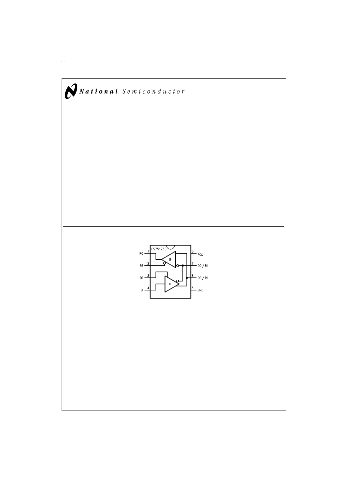
Connection and Logic Diagram
TRI-STATE®is a registered trademark of National Semiconductor Corp.
DS008759-1
Top View
Order Number DS75176BN, DS75176BTN, DS75176BM or DS75176BTM
See NS Package Number N08E or M08A
July 1998
DS75176B/DS75176BT Multipoint RS-485/RS-422 Transceivers
© 1999 National Semiconductor Corporation DS008759 www.national.com
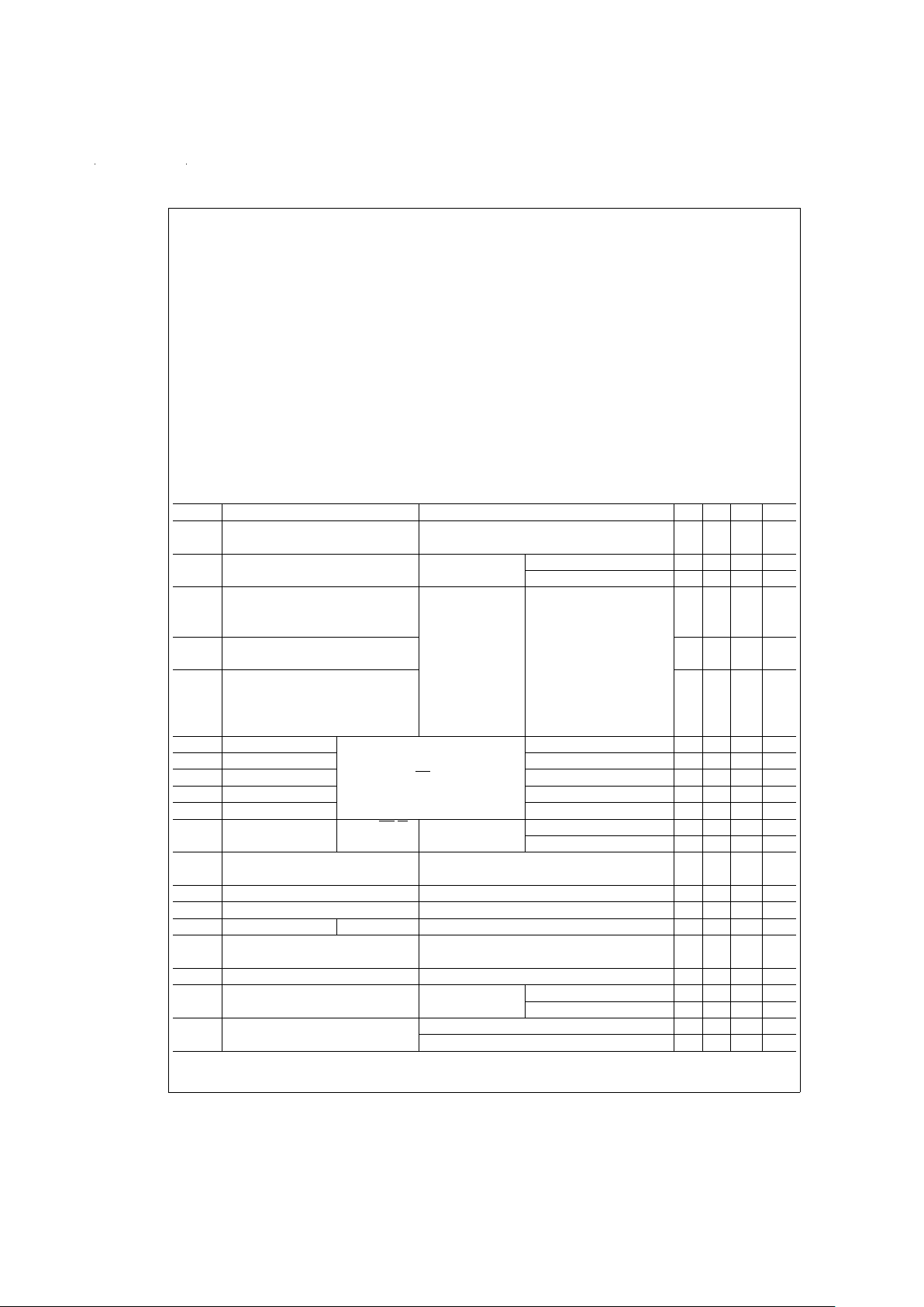
Absolute Maximum Ratings (Note 1)
If Military/Aerospace specified devices are required,
please contact the National Semiconductor Sales Office/
Distributors for availability and specifications.
Supply Voltage, V
CC
7V
Control Input Voltages 7V
Driver Input Voltage 7V
Driver Output Voltages +15V/ −10V
Receiver Input Voltages (DS75176B) +15V/ −10V
Receiver Output Voltage 5.5V
Continuous Power Dissipation
@
25˚C
for M Package 675 mW (Note 5)
for N Package 900 mW (Note 4)
Storage Temperature Range −65˚C to +150˚C
Lead Temperature
(Soldering, 4 seconds) 260˚C
Recommended Operating
Conditions
Min Max Units
Supply Voltage, V
CC
4.75 5.25 V
Voltage at Any Bus Terminal −7 +12 V
(Separate or Common Mode)
Operating Free Air Temperature T
A
DS75176B 0 +70 ˚C
DS75176BT −40 +85 ˚C
Differential Input Voltage,
VID (Note 6) −12 +12 V
Electrical Characteristics (Notes 2, 3)
0˚C ≤ TA≤ 70˚C, 4.75V<V
CC
<
5.25V unless otherwise specified
Symbol Parameter Conditions Min Typ Max Units
V
OD1
Differential Driver Output IO=0 5 V
Voltage (Unloaded)
V
OD2
Differential Driver Output (
Figure 1
) R=50Ω; (RS-422) (Note 7) 2 V
Voltage (with Load) R = 27Ω; (RS-485) 1.5 V
∆V
OD
Change in Magnitude of Driver
Differential Output Voltage For 0.2 V
Complementary Output States
V
OC
Driver Common Mode Output (
Figure 1
) R=27Ω 3.0 V
Voltage
∆|V
OC
| Change in Magnitude of Driver
Common Mode Output Voltage 0.2 V
For Complementary Output
States
V
IH
Input High Voltage 2V
V
IL
Input Low Voltage DI, DE, 0.8
V
CL
Input Clamp Voltage RE , E IIN= −18 mA −1.5
I
IL
Input Low Current VIL= 0.4V −200 µA
I
IH
Input High Current VIH= 2.4V 20 µA
I
IN
Input DO/RI, DO/RI VCC= 0V or 5.25V VIN= 12V +1.0 mA
Current DE = 0V V
IN
= −7V −0.8 mA
V
TH
Differential Input Threshold −7V ≤ VCM≤ + 12V −0.2 +0.2 V
Voltage for Receiver
∆V
TH
Receiver Input Hysteresis VCM=0V 70 mV
V
OH
Receiver Output High Voltage IOH= −400 µA 2.7 V
V
OL
Output Low Voltage RO IOL= 16 mA (Note 7) 0.5 V
I
OZR
OFF-State (High Impedance) VCC= Max
±
20 µA
Output Current at Receiver 0.4V ≤ V
O
≤ 2.4V
R
IN
Receiver Input Resistance −7V ≤ VCM≤ +12V 12 kΩ
I
CC
Supply Current No Load Driver Outputs Enabled 55 mA
(Note 7) Driver Outputs Disabled 35 mA
I
OSD
Driver Short-Circuit VO= −7V (Note 7) −250 mA
Output Current V
O
= +12V (Note 7) +250 mA
www.national.com 2
Electrical Characteristics (Notes 2, 3) (Continued)
0˚C ≤ TA≤ 70˚C, 4.75V<V
CC
<
5.25V unless otherwise specified
Symbol Parameter Conditions Min Typ Max Units
I
OSR
Receiver Short-Circuit VO= 0V −15 −85 mA
Output Current
Note 1: “Absolute Maximum Ratings” are those beyond which the safety of the device cannot be guaranteed. They are not meant to imply that the device should
be operated at these limits. The tables of “Electrical Characteristics” provide conditions for actual device operation.
Note 2: All currents into device pins are positive; all currents out of device pins are negative. All voltages are referenced to device ground unless otherwise specified.
Note 3: All typicals are given for V
CC
= 5V and TA= 25˚C.
Note 4: Derate linearly at 5.56 mW/˚C to 650 mW at 70˚C.
Note 5: Derate linearly 6.11 mW/˚C to 400 mW at 70˚C.
Note 6: Differential - Input/Output bus voltage is measured at the noninverting terminal A with respect to the inverting terminal B.
Note 7: All worst case parameters for which note 7 is applied, must be increased by 10%for DS75176BT. The other parameters remain valid for −40˚C
<
T
A
<
+85˚C.
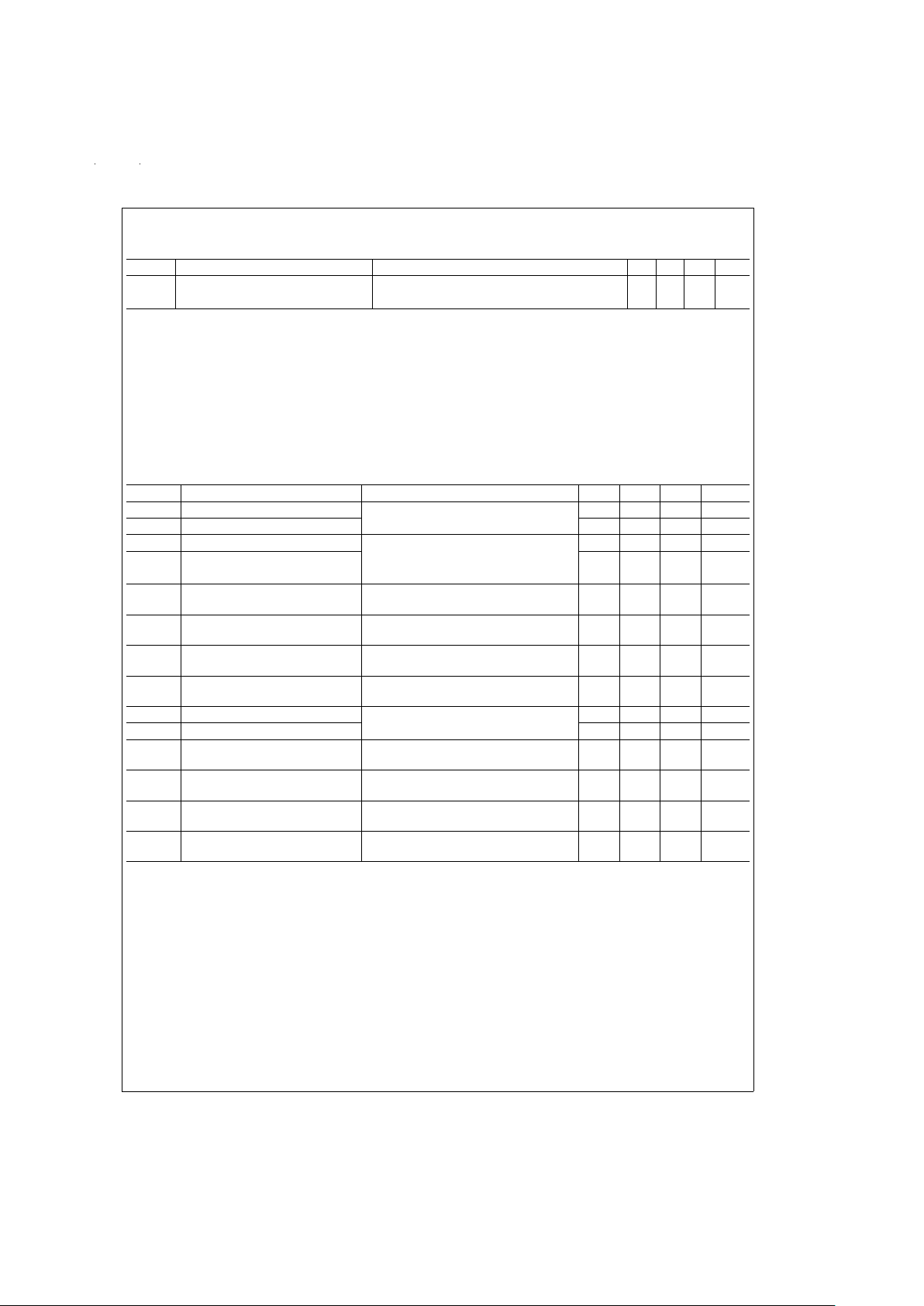
Switching Characteristics
VCC= 5.0V, TA= 25˚C
Symbol Parameter Conditions Min Typ Max Units
t
PLH
Driver Input to Output R
LDIFF
=60Ω 12 22 ns
t
PHL
Driver Input to Output CL1=CL2= 100 pF 17 22 ns
t
r
Driver Rise Time R
LDIFF
=60Ω 18 ns
t
f
Driver Fall Time CL1=CL2= 100 pF 18 ns
(
Figure 3
and
Figure 5
)
t
ZH
Driver Enable to Output High CL= 100 pF (
Figure 4
and
Figure 6
)S1
Open
29 100 ns
t
ZL
Driver Enable to Output Low CL= 100 pF (
Figure 4
and
Figure 6
)S2
Open
31 60 ns
t
LZ
Driver Disable Time from Low CL=15pF(
Figure 4
and
Figure 6
)S2
Open
13 30 ns
t
HZ
Driver Disable Time from High CL=15pF(
Figure 4
and
Figure 6
)S1
Open
19 200 ns
t
PLH
Receiver Input to Output CL=15pF(
Figure 2
and
Figure 7
)3037ns
t
PHL
Receiver Input to Output S1 and S2 Closed 32 37 ns
t
ZL
Receiver Enable to Output Low CL=15pF(
Figure 2
and
Figure 8
)S2
Open
15 20 ns
t
ZH
Receiver Enable to Output High CL=15pF(
Figure 2
and
Figure 8
)S1
Open
11 20 ns
t
LZ
Receiver Disable from Low CL=15pF(
Figure 2
and
Figure 8
)S2
Open
28 32 ns
t
HZ
Receiver Disable from High CL=15pF(
Figure 2
and
Figure 8
)S1
Open
13 35 ns
www.national.com3

AC Test Circuits
Switching Time Waveforms
DS008759-2
FIGURE 1.
DS008759-3
Note: S1 and S2 of load circuit are closed except as otherwise mentioned.
FIGURE 2.
DS008759-4
FIGURE 3.
DS008759-5
Note: Unless otherwise specified the switches are closed.
FIGURE 4.
DS008759-6
FIGURE 5. Driver Propagation Delays and Transition Times
www.national.com 4

Switching Time Waveforms (Continued)
Function Tables
DS75176B Transmitting
Inputs Line Outputs
RE
DE DI Condition DO DO
X 1 1 No Fault 0 1
X 1 0 No Fault 1 0
X0X X ZZ
X 1 X Fault Z Z
DS008759-7
FIGURE 6. Driver Enable and Disable Times
DS008759-8
Note: Differential input voltage may may be realized by grounding RI and pulsing RI between +2.5V and −2.5V
FIGURE 7. Receiver Propagation Delays
DS008759-9
FIGURE 8. Receiver Enable and Disable Times
www.national.com5

Function Tables (Continued)
DS75176B Receiving
Inputs Outputs
RE
DE RI-RI RO
00 ≥+0.2V 1
00 ≤−0.2V 0
0 0 Inputs Open** 1
10 X Z
X — Don’t care condition
Z — High impedance state
Fault — Improper line conditons causing excessive power dissipation in the driver, such as shorts or bus contention
situations
**This is a fail safe condition
Typical Application
DS008759-11
www.national.com 6

Physical Dimensions inches (millimeters) unless otherwise noted
Lit. # 103669
Molded Dual-In-Line Package (N)
Order Number DS75176BN or DS75176BTN
NS Package Number N08E
www.national.com7

LIFE SUPPORT POLICY
NATIONAL’S PRODUCTS ARE NOT AUTHORIZED FOR USE AS CRITICAL COMPONENTS IN LIFE SUPPORT DEVICES OR SYSTEMS WITHOUT THE EXPRESS WRITTEN APPROVAL OF THE PRESIDENT OF NATIONAL SEMICONDUCTOR CORPORATION. As used herein:
1. Life support devices or systems are devices or systems which, (a) are intended for surgical implant into
the body, or (b) support or sustain life, and whose failure to perform when properly used in accordance
with instructions for use provided in the labeling, can
be reasonably expected to result in a significant injury
to the user.
2. A critical component is any component of a life support
device or system whose failure to perform can be reasonably expected to cause the failure of the life support
device or system, or to affect its safety or effectiveness.
National Semiconductor
Corporation
Americas
Tel: 1-800-272-9959
Fax: 1-800-737-7018
Email: support@nsc.com
www.national.com
National Semiconductor
Europe
Fax: +49 (0) 1 80-530 85 86
Email: europe.support@nsc.com
Deutsch Tel: +49 (0) 1 80-530 85 85
English Tel: +49 (0) 1 80-532 78 32
Français Tel: +49 (0) 1 80-532 93 58
Italiano Tel: +49 (0) 1 80-534 16 80
National Semiconductor
Asia Pacific Customer
Response Group
Tel: 65-2544466
Fax: 65-2504466
Email: sea.support@nsc.com
National Semiconductor
Japan Ltd.
Tel: 81-3-5639-7560
Fax: 81-3-5639-7507
DS75176B/DS75176BT Multipoint RS-485/RS-422 Transceivers
National does not assume any responsibility for use of any circuitry described, no circuit patent licenses are implied and National reserves the right at any time without notice to change said circuitry and specifications.
 Loading...