

NSC DS3695N, DS3695MWC Datasheet
DS3695/DS3695T/DS3696/DS3697
Multipoint RS485/RS422 Transceivers/Repeaters
General Description
The DS3695, DS3696, and DS3697 are high speed differential TRI-STATE
®
bus/line transceivers/repeaters designed to
meet the requirementsofEIAstandard RS485 with extended
common mode range (+12V to −7V), for multipoint data
transmission.
The driver and receiver outputs feature TRI-STATE capability. The driver outputs remain in TRI-STATE over the entire
common mode range of +12V to −7V. Bus faults that cause
excessive power dissipation within the device trigger a thermal shutdown circuit, which forces the driver outputs into the
high impedance state. The DS3696 provides an output pin
TS (thermal shutdown) which reports the occurrence of the
thermal shutdown of the device. This is an “open collector”
pin with aninternal10kΩ pull-up resistor. This allows the line
fault outputs of several devices to be wire OR-ed.
Both AC and DC specifications are guaranteed over the 0˚C
to 70˚C temperature and 4.75V to 5.25V supply voltage
range.
Features
n Meets EIA standard RS485 for multipoint bus
transmission and is compatible with RS-422
n 15 ns driver propagation delays with 2 ns skew (typical)
n Single +5V supply
n −7V to +12V bus common mode range permits
±
7V
ground difference between devices on the bus
n Thermal shutdown protection
n High impedance to bus with driver in TRI-STATE or with
power off, over the entire common mode range allows
the unused devices on the bus to be powered down
n Combined impedance of a driver output and receiver
input is less than one RS485 unit load, allowing up to 32
transceivers on the bus
n 70 mV typical receiver hysteresis
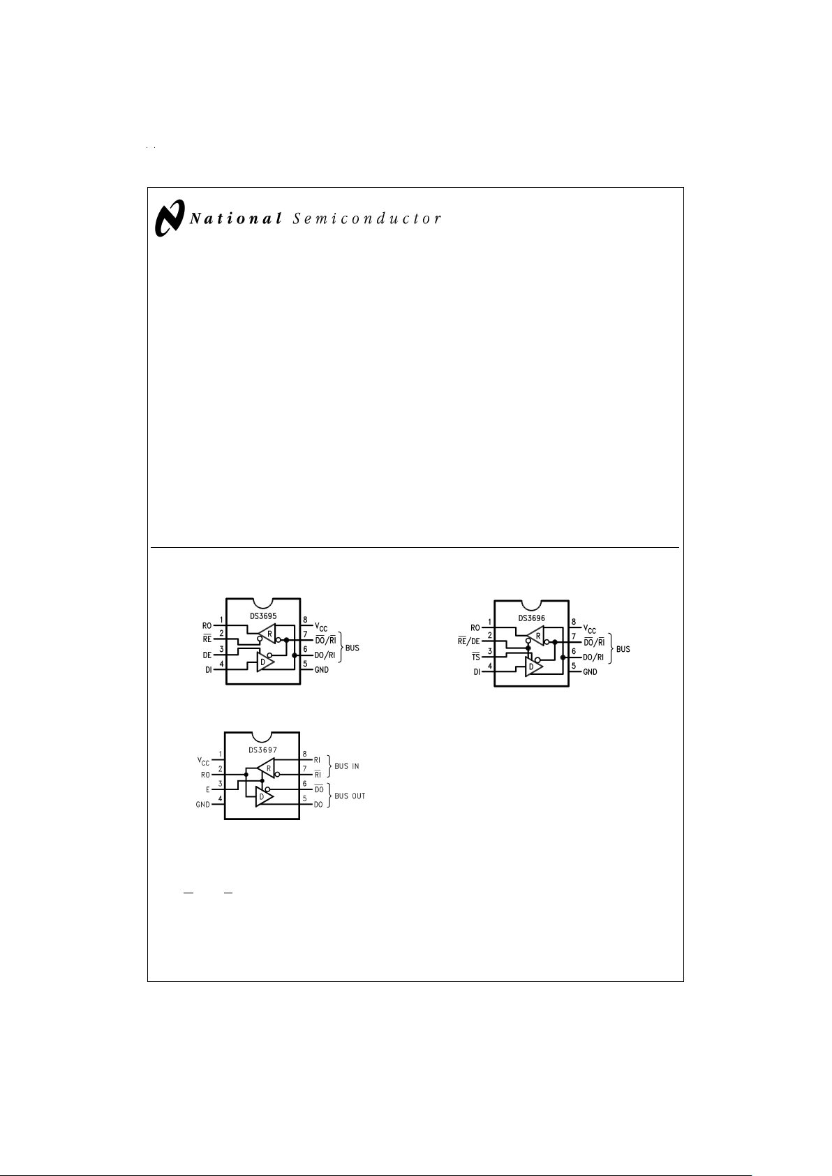
Connection and Logic Diagrams
Note 1: TS pin was LF (Line Fault) in previous datasheets and reports the occurrence of a thermal shutdown of the device.
TRI-STATE®is a registered trademark of National Semiconductor Corporation.
DS010408-1
Top View
DS010408-12
Top View
DS010408-13
Top View
Order Number DS3695N, DS3695TN,
DS3696N, or DS3697N
See NS Package Number N08E
May 1998
DS3695/DS3695T/DS3696/DS3697 Multipoint RS485/RS422 Transceivers/Repeaters
© 1998 National Semiconductor Corporation DS010408 www.national.com
Absolute Maximum Ratings (Note 2)
If Military/Aerospace specified devices are required,
please contact the National Semiconductor Sales Office/
Distributors for availability and specifications.
Supply Voltage, V
CC
7V
Control Input Voltages 7V
Driver Input Voltage 7V
Driver Output Voltages +15V/−10V
Receiver Input Voltages
(DS3695, DS3696) +15V/−10V
Receiver Common Mode Voltage
(DS3697)
±
25V
Receiver Output Voltage 5.5V
Continuous Power Dissipation
@
25˚C
N Package 1.07W (Note
4)
Storage Temperature Range −65˚C to
+150˚C
Lead Temperature (Soldering, 4
sec.) 260˚C
Recommended Operating
Conditions
Min Max Units
Supply Voltage, V
CC
4.75 5.25 V
Bus Voltage −7 +12 V
Operating Free Air Temp. (T
A
)
Commercial 0 +70 ˚C
Industrial −40 +85 ˚C
Electrical Characteristics (Notes 3, 4)
0˚C ≤ TA≤ +70˚C, 4.75V<V
CC
<
5.25V unless otherwise specified
Symbol Parameter Conditions Min Typ Max Units
V
OD1
Differential Driver Output I
O
=
05V
Voltage (Unloaded)
V
OD2
Differential Driver Output (
Figure 1
)R
=
50Ω; (RS-422) (Note6)2V
Voltage (with Load) R=27Ω; (RS-485) 1.5 V
∆V
OD
Change in Magnitude of Driver
Differential Output Voltage for 0.2 V
Complementary Output States
V
OC
Driver Common Mode Output Voltage (
Figure 1
)R
=
27Ω 3.0 V
∆|V
OC
| Change in Magnitude of Driver
Common Mode Output Voltage 0.2 V
for Complementary Output States
V
IH
Input High Voltage 2V
V
IL
Input Low Voltage DI, DE, 0.8 V
V
CL
Input Clamp Voltage RE , E, RE /DE I
IN
=
−18 mA −1.5 V
I
IL
Input Low Current V
IL
=
0.4V −200 µA
I
IH
Input High Current V
IH
=
2.4V 20 µA
I
IN
Input Current DO/RI, DO /RI V
CC
=
0V or
5.25V
V
IN
=
12V +1.0 mA
RI, RI
RE /DE or DE
=
0V
V
IN
=
−7V −0.8 mA
I
OZD
TRI-STATE Current DO, DO V
CC
=
0V or 5.25V, E=0V
±
100 µA
DS3697 & DS3698 −7V
<
V
O
<
+12V
V
TH
Differential Input Threshold −7V ≤ VCM≤ +12V −0.2 +0.2 V
Voltage for Receiver
∆V
TH
Receiver Input Hysteresis V
CM
=
0V 70 mV
V
OH
Receiver Output High Voltage I
OH
=
−400 µA 2.4 V
V
OL
Output Low Voltage RO I
OL
=
16 mA (Note 6) 0.5 V
TS
I
OL
=
8 mA 0.45 V
I
OZR
OFF-State (High Impedance) V
CC
=
Max
±
20 µA
Output Current at Receiver 0.4V ≤ V
O
≤ 2.4V
R
IN
Receiver Input Resistance −7V ≤ VCM≤ +12V 12 kΩ
www.national.com 2
Electrical Characteristics (Notes 3, 4) (Continued)
0˚C ≤ TA≤ +70˚C, 4.75V<V
CC
<
5.25V unless otherwise specified
Symbol Parameter Conditions Min Typ Max Units
I
CC
Supply Current No Load Driver Outputs Enabled 42 60 mA
(Note 6) Driver Outputs Disabled 27 40 mA
I
OSD
Driver Short-Circuit Output Current V
O
=
−7V (Note 6) −250 mA
V
O
=
+12V (Note 6) +250 mA
I
OSR
Receiver Short-Circuit Output Current V
O
=
0V −15 −85 mA
Note 2: “Absolute Maximum Ratings” are those beyond which the safety of the device cannot be guaranteed. They are not meant to imply that the device should
be operated at these limits. The tables of “Electrical Characteristics” provide conditions for actual device operation.
Note 3: All currents into device pins are positive; all currents out of device pins are negative. All voltages are referenced to device ground unless otherwise specified.
Note 4: All typicals are given for V
CC
=
5V and T
A
=
25˚C.
Note 5: Derate linearly at 11.1 mW/˚C to 570 mW at 70˚C.
Note 6: All limits for which Note 5 is applied must be derated by 10%for DS3695T and DS3696T. Other parameters remain the same for this extended temperature
range device (−40˚C ≤ T
A
≤ +85˚C).
Switching Characteristics (Notes 4, 7) 0˚C ≤ T
A
≤ +70˚C, 4.75V<V
CC
<
5.25V unless otherwise specified
Receiver Switching Characteristics
(
Figures 2, 3, 4
)
Symbol Conditions Min Typ Max Units
t
PLH
C
L
=
15 pF 15 25 37 ns
t
PHL
S1 and S2 15 25 37 ns
|t
PLH–tPHL
| Closed 0 ns
t
PLZ
C
L
=
15 pF, S2 Open 5 12 16 ns
t
PHZ
C
L
=
15 pF, S1 Open 5 12 16 ns
t
PZL
C
L
=
15 pF, S2 Open 7 15 20 ns
t
PZH
C
L
=
15 pF, S1 Open 7 15 20 ns
Driver Switching Characteristics
Symbol Conditions Min Typ Max Units
SINGLE ENDED CHARACTERISTICS (
Figures 5, 6, 7
)
t
PLH
RLDIFF=60Ω 91522 ns
t
PHL
C
L1
=
C
L2
=
100 pF 9 15 22 ns
t
SKEW|tPLH–tPHL
|28ns
t
PLZ
C
L
=
15 pF, S2 Open 7 15 30 ns
t
PHZ
C
L
=
15 pF, S1 Open 7 15 30 ns
t
PZL
C
L
=
100 pF, S2 Open 30 35 50 ns
t
PZH
C
L
=
100 pF, S1 Open 30 35 50 ns
DIFFERENTIAL CHARACTERISTICS (
Figures 5, 8
)
t
r,tf
RLDIFF=60Ω 61018 ns
C
L1
=
C
L2
=
100 pF
Note 7: Switching Characteristics apply for DS3695, DS3695T, DS3696, DS3697 only.
www.national.com3
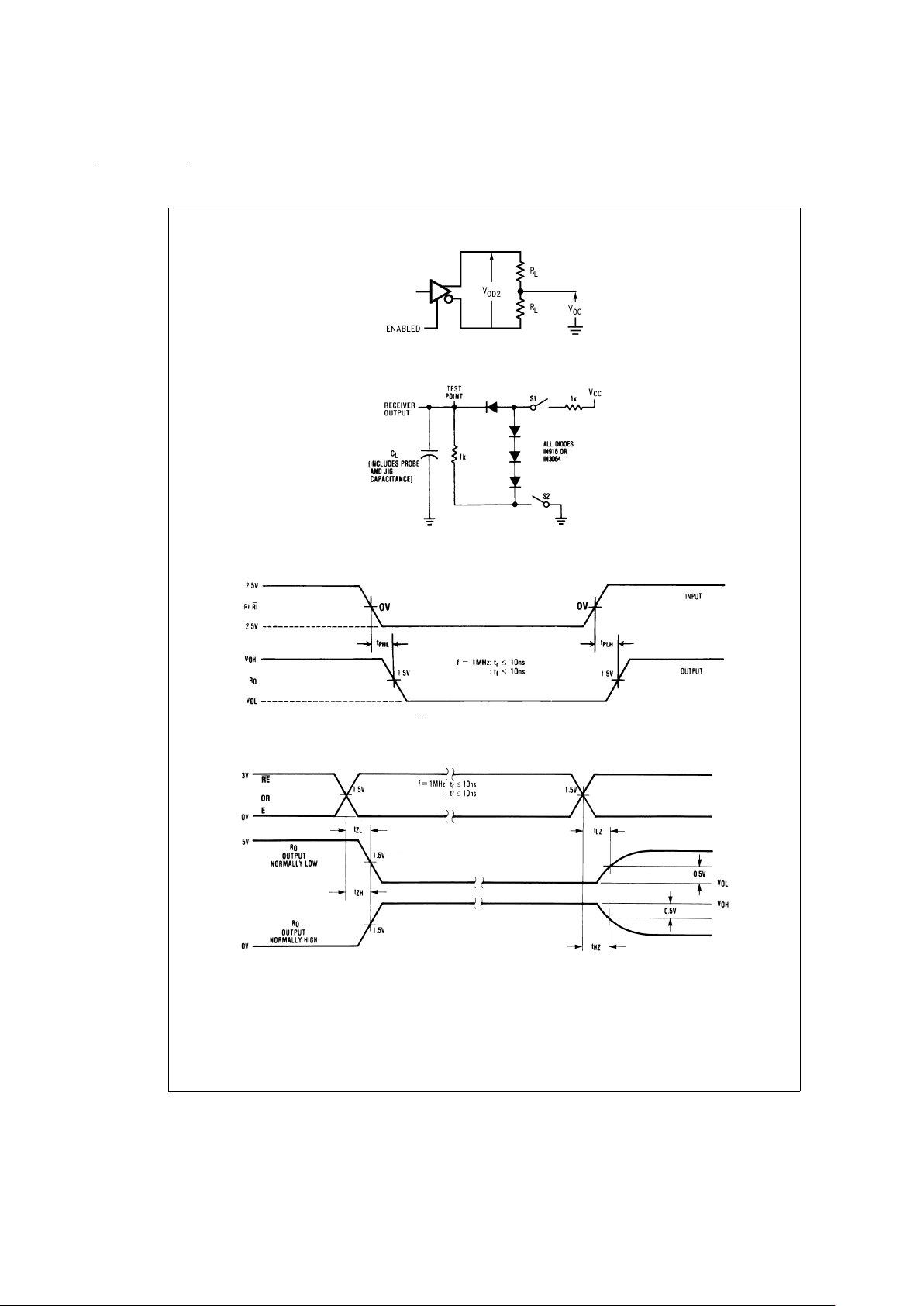
AC Test Circuits and Switching Waveforms
DS010408-15
FIGURE 1. Driver VODand V
OC
DS010408-3
FIGURE 2. Receiver Propagation Delay Test Circuit
DS010408-4
Note: Differential input voltage may be realized by grounding RI and pulsing RI between +2.5V and −2.5V.
FIGURE 3. Receiver Input-to-Output Propagation Delay Timing
DS010408-5
FIGURE 4. Receiver Enable/Disable Propagation Delay Timing
www.national.com 4
 Loading...