

NSC DS36954VX, DS36954V, DS36954MX, DS36954M Datasheet

DS36954
Quad Differential Bus Transceiver
General Description
The DS36954 is a low power, quad EIA-485 differential bus
transceiver especially suited for high speed, parallel, multipoint, I/O bus applications.A compact 20-pin surface mount
PLCC or SOIC package provides high transceiver integration and a very small PC board footprint.
Propagation delay skew between devices is specified to aid
in parallel interface designs— limits on maximum and minimum delay times are guaranteed.
Five devices can implement a complete SCSI initiator or target interface. Three transceivers in a package are pinned out
for data bus connections. The fourth transceiver, with the
flexibility provided by its individual enables, can serve as a
control bus transceiver.
Features
n Pinout for SCSI interface
n Compact 20-pin PLCC or SOIC package
n Meets EIA-485 standard for multipoint bus transmission
n Greater than 60 mA source/sink currents
n Thermal shutdown protection
n Glitch-free driver outputs on power up and down
Connection Diagrams Logic Diagrams
TRI-STATE®is a registered trademark of National Semiconductor Corporation.
DS011014-1
Order Number DS36954V
See NS Package Number V20A
DS011014-19
Order Number DS36954M
See NS Package Number M20B
DS011014-2
July 1998
DS36954 Quad Differential Bus Transceiver
© 1999 National Semiconductor Corporation DS011014 www.national.com
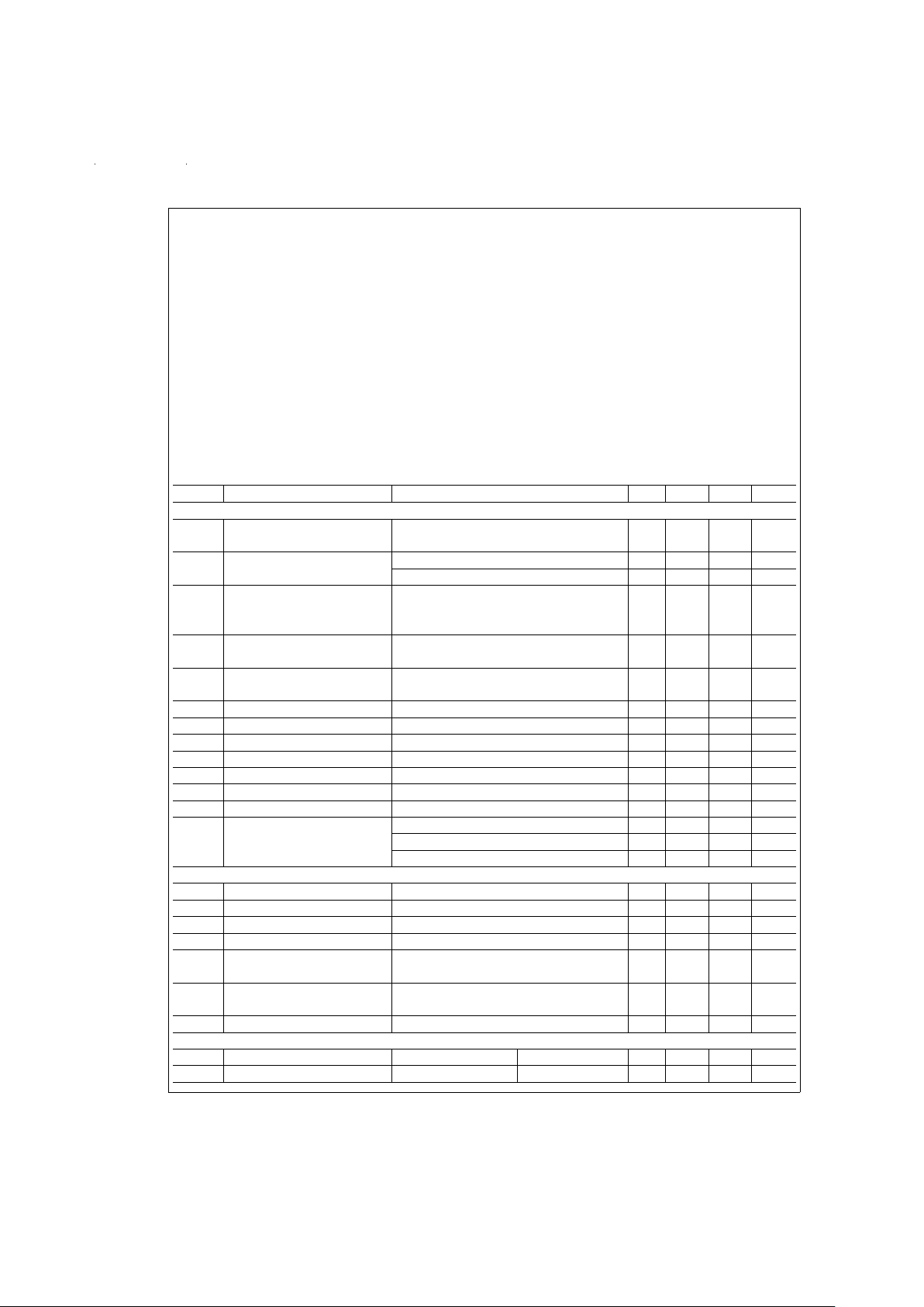
Absolute Maximum Ratings (Note 1)
If Military/Aerospace specified devices are required,
please contact the National Semiconductor Sales Office/
Distributors for availability and specifications.
Supply Voltage 7V
Control Input Voltage V
CC
+ 0.5V
Driver Input Voltage V
CC
+ 0.5V
Driver Output Voltage/
Receiver Input Voltage −10V to +15V
Receiver Output Voltage 5.5V
Continuous Power Dissipation
@
+25˚C
V Package 1.73W
M Package 1.73W
Derate V Package 13.9 mW/˚C above +25˚C
Derate M Package 13.7 mW/˚C above +25˚C
Storage Temperature Range −65˚C to +150˚C
Lead Temperature
(Soldering 4 Sec.) 260˚C
Recommended
Operating Conditions
Min Max Units
Supply Voltage, V
CC
4.75 5.25 V
Bus Voltage −7 +12 V
Operating Free Air
Temperature (T
A
) 0 +70 ˚C
Electrical Characteristics (Note 2)
Over Supply Voltage and Operating Temperature ranges, unless otherwise specified
Symbol Parameter Conditions Min Typ Max Units
DRIVER CHARACTERISTICS
V
ODL
Differential Driver Output I
L
=
60 mA 1.5 1.9 V
Voltage (Full Load) V
CM
=
0V
V
OD
Differential Driver Output R
L
=
100Ω (EIA-422) 2.0 2.25 V
Voltage (Termination Load) R
L
=
54Ω (EIA-485) 1.5 2.0 V
∆IVODI Change in Magnitude of Driver R
L
=
54 or 100Ω
Differential Output Voltage for (Note 4)
(Figure 1 )
0.2 V
Complementary Output States (EIA-422/485)
V
OC
Driver Common Mode R
L
=
54Ω
(Figure 1 )
(EIA-485) 3.0 V
Output Voltage (Note 5)
∆IVOCI Change in Magnitude of (Note 4)
(Figure 1 )
0.2 V
Common Mode Output Voltage (EIA-422/485)
V
OH
Output Voltage High I
OH
=
−55 mA 2.7 3.2 V
V
OL
Output Voltage Low I
OL
=
55 mA 1.4 1.7 V
V
IH
Input Voltage High 2.0 V
V
IL
Input Voltage Low 0.8 V
V
CL
Input Clamp Voltage I
CL
=
−18 mA −1.5 V
I
IH
Input High Current V
IN
=
2.4V (Note 3) 20 µA
I
IL
Input Low Current V
IN
=
0.4V (Note 3) −20 µA
I
OSC
Driver Short-Circuit V
O
=
−7V (EIA-485) −130 −250 mA
Output Current V
O
=
0V (EIA-422) −90 −150 mA
(Note 9) V
O
=
+12V (EIA-485) 130 250 mA
RECEIVER CHARACTERISTICS
I
OSR
Short Circuit Output Current V
O
=
0V (Note 9) −15 −28 −75 mA
I
OZ
TRI-STATE®Output Current V
O
=
0.4V to 2.4V 20 µA
V
OH
Output Voltage High V
ID
=
0.2V, I
OH
=
0.4 mA 2.4 3.0 V
V
OL
Output Voltage Low V
ID
=
−0.2V, I
OL
=
4 mA 0.35 0.5 V
V
TH
Differential Input High V
O
=
V
OH,IO
=
−0.4 mA 0.03 0.2 V
Threshold Voltage (EIA-422/485)
V
TL
Differential Input Low V
O
=
V
OL,IO
=
4.0 mA −0.20 −0.03 V
Threshold Voltage (Note 6) (EIA-422/485)
V
HST
Hysteresis (Note 7) V
CM
=
0V 35 60 mV
DRIVER AND RECEIVER CHARACTERISTICS
V
IH
Enable Input Voltage High 2.0 V
V
IL
Enable Input Voltage Low 0.8 V
www.national.com 2
Electrical Characteristics (Note 2) (Continued)
Over Supply Voltage and Operating Temperature ranges, unless otherwise specified
Symbol Parameter Conditions Min Typ Max Units
DRIVER AND RECEIVER CHARACTERISTICS
V
CL
Enable Input Clamp Voltage I
CL
=
−18 mA −1.5 V
I
IN
Line Input Current Other Input=0V V
I
=
+12V 0.5 1.0 mA
(Note 8) DE/RE=0.8V
V
I
=
−7V −0.45 −0.8 mA
DE4=0.8V
I
ING
Line Input Current Other Input=0V V
I
=
+12V 1.0 mA
(Note 8) DE/RE and DE4=2V
V
CC
=
3.0V V
I
=
−7V −0.8 mA
T
A
=
+25˚C
I
IH
Enable Input V
IN
=
2.4V V
CC
=
3.0V 1 40 µA
Current High DE/RE
V
CC
=
4.75V 1 µA
V
CC
=
5.25V 1 40 µA
V
IN
=
2.4V V
CC
=
3.0V 1 20 µA
DE4 or RE4
V
CC
=
5.25V 1 20 µA
I
IL
Enable Input V
IN
=
0.8V V
CC
=
3.0V −6 −40 µA
Current Low DE/RE
V
CC
=
4.75V −12 µA
V
CC
=
5.25V −14 −40 µA
V
IN
=
0.8V V
CC
=
3.0V −3 −20 µA
DE4 or RE4
V
CC
=
5.25V −7 −20 µA
I
CCD
Supply Current (Note 10) No Load, DE/RE and DE4=2.0V 75 90 mA
I
CCR
Supply Current (Note 10) No Load, DE/RE and RE4=0.8V 50 70 mA
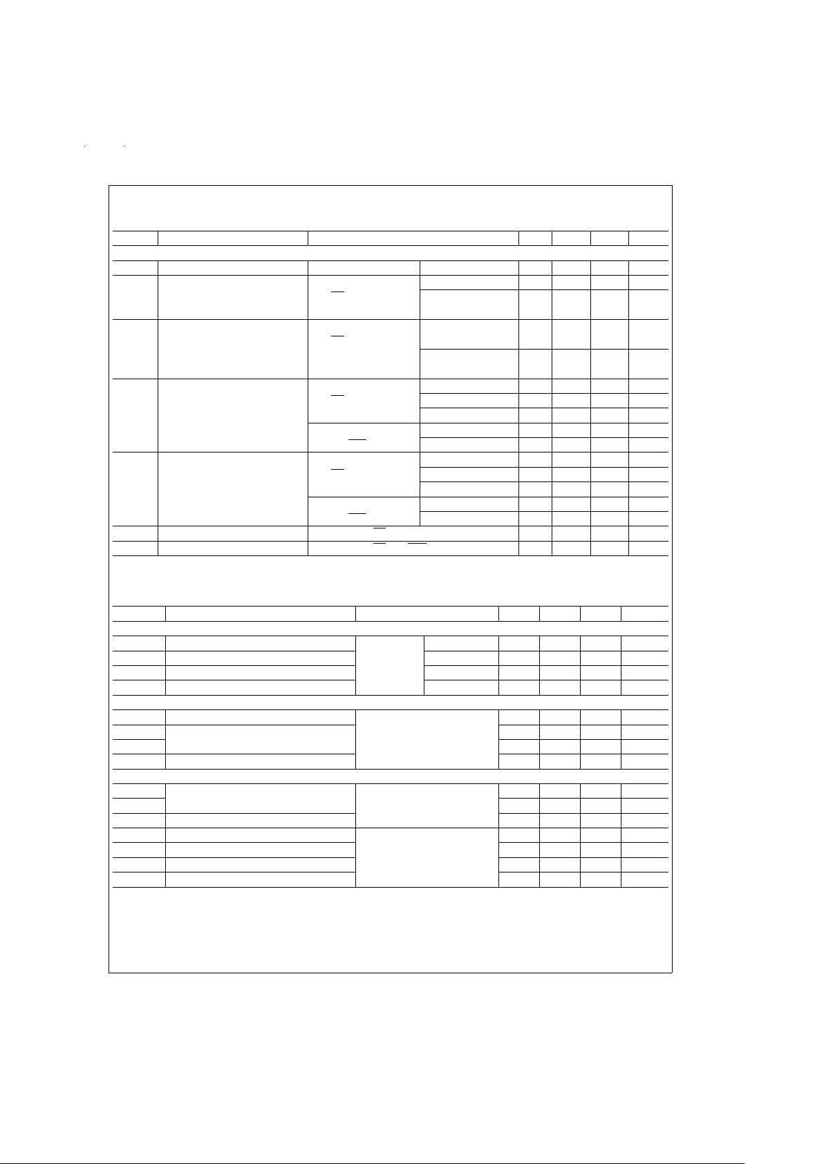
Switching Characteristics
Over Supply Voltage and Operating Temperature ranges, unless otherwise specified.
Symbol Parameter Conditions Min Typ Max Units
DRIVER SINGLE-ENDED CHARACTERISTICS
t
PZH
Output Enable Time to High Level R
L
=
110Ω (
Figure 5
)3540ns
t
PZL
Output Enable Time to Low Level (
Figure 6
)2540ns
t
PHZ
Output Disable Time to High Level (
Figure 5
)1525ns
t
PLZ
Output Disable Time to Low Level (
Figure 6
)3540ns
DRIVER DIFFERENTIAL CHARACTERISTICS
t
r,tf
Rise and Fall Time R
L
=
54Ω 13 16 ns
t
PLHD
Differential Propagation C
L
=
50 pF 9 15 19 ns
t
PHLD
Delays (Note 15) C
D
=
15 pF 9 12 19 ns
t
SKD
|t
PLHD−tPHLD
| Diff. Skew (
Figures 3, 4, 9
)36ns
RECEIVER CHARACTERISTICS
t
PLHD
Differential Propagation Delays C
L
=
15 pF 9 14 19 ns
t
PHLD
V
CM
=
2.0V 9 13 19 ns
t
SKD
|t
PLHD−tPHLD
| Diff. Receiver Skew (
Figure 7
)13ns
t
PZH
Output Enable Time to High Level C
L
=
15 pF 15 22 ns
t
PZL
Output Enable Time to Low Level (
Figure 8
)2030ns
t
PHZ
Output Disable Time from High Level 20 30 ns
t
PLZ
Output Disable Time from Low Level 17 25 ns
Note 1: “Absolute Maximum Ratings” are those values beyond which the safety of the device cannot be guaranteed. They are not meant to imply that the devices
should be operated at these limits. The tables of “Electrical Characteristics” specify conditions for device operation.
Note 2: Current into device pins isdefinedaspositive.Currentoutof device pins is defined as negative.Allvoltagesarereferencedto ground unless otherwise specified.
Note 3: I
IH
and IILinclude driver input current and receiver TRI-STATE leakage current on DR(1–3).
Note 4: ∆ IVODI and ∆ IVOCI are changes in magnitude of V
OD
and VOC, respectively, that occur when the input changes state.
www.national.com3
 Loading...