DS1692/DS3692
TRI-STATE
General Description
The DS1692/DS3692 are low power Schottky TTL line drivers electrically similarto the DS1691A/DS3691 but tested to
meet the requirements of MIL-STD-188-114A (see Application Note AN-216). MIL-STD-188-114A type 1 driver specifications can be met by adding an external three resistor voltage divider to the output of the DS3692/1692. The DS3692/
1692 feature 4 buffered outputs with high source and sink
current capability with internal short circuit protection.
With the mode select pin low, the DS1692/DS3692 are dual
differential line drivers with TRI-STATE outputs. They feature
±
10V output common-mode range in TRI-STATE and 0V
output unbalance when operated with
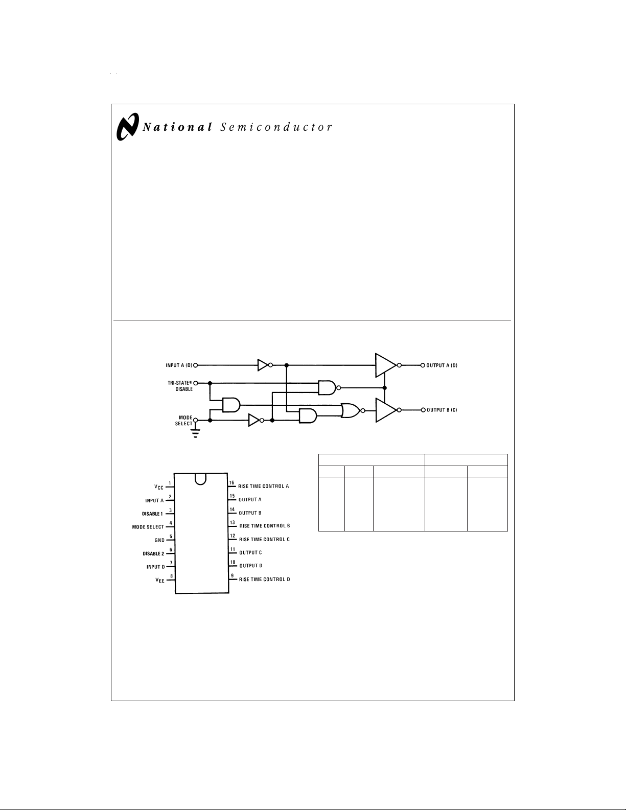
Logic Diagram (1⁄2Circuit Shown)
®
Differential Line Drivers
±
5V supply.
March 1992
Multipoint applications in differential mode with waveshaping
capacitors is not allowed.
Features
n Short circuit protection for both source and sink outputs
n 100Ω transmission line drive capability
n Low I
n Low current PNP inputs compatible with TTL, MOS and
n Adaptable as MIL-STD-188-114A type 1 driver
and IEEpower consumption: Differential
CC
mode: I
CMOS
=
9 mA/driver typ, I
CC
=
5 mA/driver typ
EE
DS1692/DS3692 TRI-STATE Differential Line Drivers
DS005784-1
Connection Diagram
Mode A (D) Disable1 (2) A (D) B (C)
00 0 0 1
0 0 1 TRI-STATE TRI-STATE
01 0 1 0
0 1 1 TRI-STATE TRI-STATE
*Contact Product Marketing for availability.
Top View
Order Number DS1692J, DS3692J,
DS3692M or DS3692N
See NS Package Number J16A, M16A
TRI-STATE®is a registered trademark of National Semiconductor Corporation.
© 1999 National Semiconductor Corporation DS005784 www.national.com
DS005784-2
*
or N16A
Inputs Outputs

Absolute Maximum Ratings (Note 2)
If Military/Aerospace specified devices are required,
please contact the National Semiconductor Sales Office/
Distributors for availability and specifications.
Supply Voltage
V
CC
V
EE
Maximum Power Dissipation (Note 1) at 25˚C
Cavity Package 1509 mW
Molded Package 1476 mW
Input Voltage 15V
Output Voltage (Power OFF)
Storage Temperature −65˚C to +150˚C
Lead Temperature (Soldering, 4 sec.) 260˚C
±
−7V
15V
Operating Conditions
Supply Voltage
DS1692
V
7V
CC
V
EE
DS3692
V
CC
V
EE
Temperature (T
)
A
DS1692 −55 +125 ˚C
DS3692 0 +70 ˚C
Note 1: Derate cavity package 10.1 mW/˚C; derate molded package 11.9
mW/˚C above 25˚C.
Min Max Units
4.5 5.5 V
−4.5 −5.5 V
4.75 5.25 V
−4.75 −5.25 V
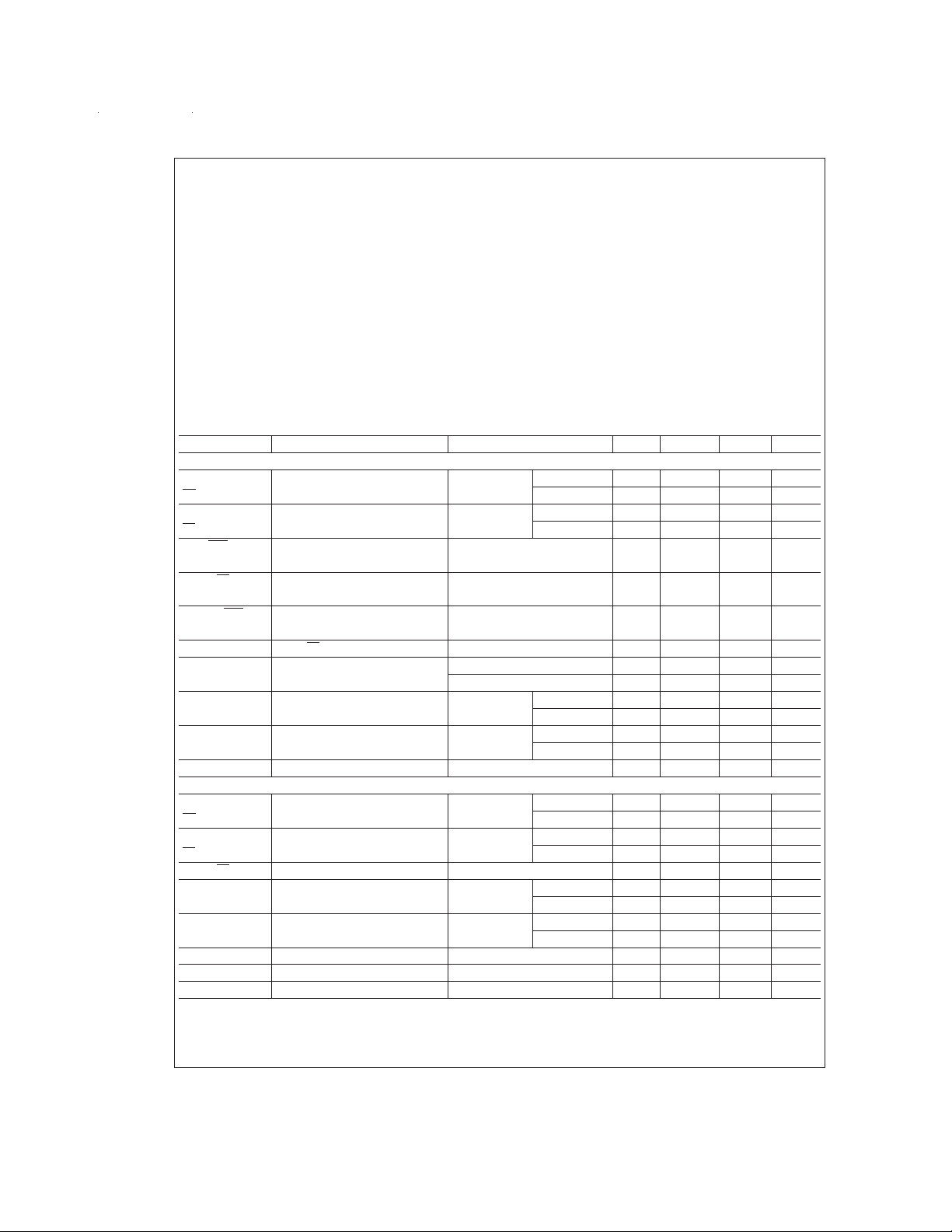
Electrical Characteristics
DS1692/DS3692 (Notes 3, 4, 5)
Symbol Parameter Conditions Min Typ Max Units
=
±
DS1692, V
V
O
V
O
V
T
V
T
V
OS,VOS
CC
10%, DS3692, V
5V
Differential Output Voltage R
V
A,B
Differential Output Voltage R
V
A,B
Common-Mode Offset R
Voltage
|V
|−|VT| Difference in Differential R
T
Output Voltage
|V
|−|VOS| Difference in Common- R
OS
Mode Offset Voltage
V
SS
I
OX
I
SA
I
SB
I
CC
DS1692, V
V
O
V
O
V
T
V
T
|V
|−|VT| Output Unbalance |VCC|=|VEE|, R
T
I
OX
+
I
S
−
I
S
I
SLEW
I
CC
I
EE
|VT−VT| R
TRI-STATE Output Current VO≤ −10V −0.002 −0.15 mA
Output Short Circuit Current V
Output Short Circuit Current V
Supply Current 18 30 mA
=
±
10%,V
5V
CC
=
EE
Differential Output Voltage R
V
A,B
Differential Output Voltage R
V
A,B
TRI-STATE Output Current V
Output Short Circuit Current V
Slew Control Current
Positive Supply Current V
Negative Supply Current V
=
CC
±
10%, DS3692, V
−5V
±
5%,VEECONNECTION TO GROUND, MODE SELECT ≤ 0.8V
5V
=
∞
L
=
100Ω V
L
VCC≥ 4.75V V
=
100Ω 2.5 3 V
L
=
100Ω 0.05 0.4 V
L
=
100Ω 0.05 0.4 V
L
=
100Ω,V
L
V
≥ 15V 0.002 0.15 mA
O
=
0.4V V
IN
=
2.4V V
IN
=
±
5%,V
5V
CC
=
∞
L
=
200Ω V
L
=
0V V
O
=
0.4V, R
IN
=
0.4V, R
IN
=
V
2V 2.5 3.6 V
IN
=
V
0.8V −2.5 −3.6 V
IN
=
2V 2 2.6 V
IN
=
0.8V −2 −2.6 V
IN
≥ 4.75V 4.0 4.8 V
CC
=
6V 80 150 mA
OA
=
V
0V −80 −150 mA
OB
=
0V −80 −150 mA
OA
=
V
6V 80 150 mA
OB
=
±
5%, MODE SELECT ≤ 0.8V
−5
EE
=
V
2.4V 7 8.5 V
IN
=
V
0.4V −7 −8.5 V
IN
=
2.4V 6 7.3 V
IN
=
V
0.4V −6 −7.3 V
IN
=
200Ω 0.02 0.4 V
L
=
10V 0.002 0.15 mA
O
=
V
−10V −0.002 −0.15 mA
O
=
2.4V −80 −150 mA
IN
=
V
0.4V 80 150 mA
IN
=
∞
L
=
∞
L
±
140 µA
18 30 mA
−10 −22 mA
www.national.com 2
 Loading...