

NSC DS3658N Datasheet

DS3658 Quad High Current Peripheral Driver
DS3658 Quad High Current Peripheral Driver
March 1995
General Description
The DS3658 quad peripheral driver is designed for those
applications where low operating power, high breakdown
voltage, high output current and low output ON voltage are
required. A unique input circuit combines TTL compatibility
with high impedance. In fact, its extreme low input current
allows it to be driven directly by a CMOS device.
The outputs are capable of sinking 600 mA each and offer a
70V breakdown. However, for inductive loads the output
should be clamped to 35V or less to avoid latch-up during
turn off (inductive fly back protectionÐrefer AN-213). An onchip clamp diode capable of handling 800 mA is provided at
each output for this purpose. In addition, the DS3658 incorporates circuitry that guarantees glitch-free power up or
down operation and a fail-safe feature which puts the output
in a high impedance state when the input is open.
The molded package is specifically constructed to allow increased power dissipation over conventional packages. The
four ground pins are directly connected to the device chip
with a special copper lead frame. When the quad driver is
soldered into a PC board, the power rating of the device
improves significantly.
Applications
Y
Relay drivers
Y
Lamp drivers
Y
Solenoid drivers
Y
Hammer drivers
Y
Stepping motor drivers
Y
Triac drivers
Connection Diagram
Dual-In-Line Package
Y
LED drivers
Y
High current, high voltage drivers
Y
Level translators
Y
Fiber optic LED drivers
Features
Y
Single saturated transistor outputs
Y
Low standby power, 10 mW typical
Y
High impedance TTL compatible inputs
Y
Outputs may be tied together for increased current capacity
Y
High output current
600 mA per output
2.4A per package
Y
No output latch-up at 35V
Y
Low output ON voltage (350 mV typ@600 mA)
Y
High breakdown voltage (70V)
Y
Open collector outputs
Y
Output clamp diodes for inductive fly back protection
Y
NPN inputs for minimal input currents (1 mA typical)
Y
Low operating power
Y
Standard 5V power supply
Y
Power up/down protection
Y
Fail safe operation
Y
2W power package
Y
Pin-for-pin compatible with SN75437
Truth Table
IN EN OUT
HH L
LH Z
HL Z
LL Z
e
H
High state
e
L
Low state
e
Z
High impedance state
Top View
TL/F/5819– 1
Order Number DS3658N
See NS Package Number N16E
C
1995 National Semiconductor Corporation RRD-B30M105/Printed in U. S. A.
TL/F/5819
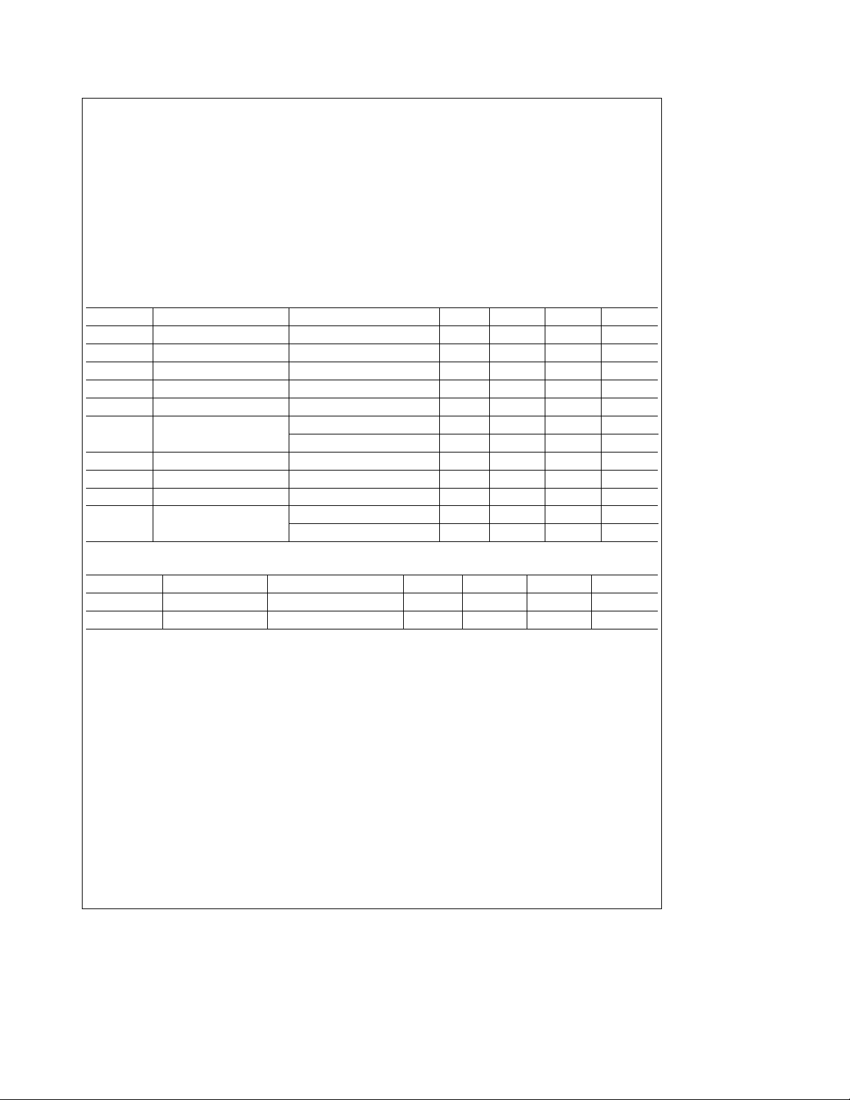
Absolute Maximum Ratings (Note 1)
If Military/Aerospace specified devices are required,
please contact the National Semiconductor Sales
Office/Distributors for availability and specifications.
Operating Conditions
Min Max Units
Supply Voltage 4.75 5.25 V
Ambient Temperature 0 70
Supply Voltage 7V
Input Voltage 15V
Output Voltage 70V
Output Current 1.5A
Continuous Power Dissipation
@
25§C Free-Air (Note 5) 2075 mW
Storage Temperature Range
b
65§Ctoa150§C
Lead Temperature (Soldering, 4 sec.) 260§C
Electrical Characteristics (Notes 2 and 3)
Symbol Parameter Conditions Min Typ Max Units
V
V
I
IH
I
IL
V
V
I
CEX
V
I
R
I
CC
IH
IL
IK
OL
F
Input High Voltage 2.0 V
Input Low Voltage 0.8 V
Input High Current V
Input Low Current V
Input Clamp Voltage I
Output Low Voltage I
Output Leakage Current V
Diode Forward Voltage I
Diode Leakage Current V
e
5.25V, V
IN
e
0.4V
IN
eb
12 mA
I
e
300 mA 0.2 0.4 V
L
e
I
600 mA (Note 4) 0.35 0.7 V
L
e
70V, V
CE
e
800 mA 1.0 1.6 V
F
e
70V 100 mA
R
e
5.25V 1.0 10 mA
CC
g
10 mA
b
0.8
e
0.8V 100 mA
IN
b
1.5 V
Supply Current All Inputs High 60 85 mA
All Inputs Low 2 4 mA
C
§
Switching Characteristics (Note 2)
Symbol Parameter Conditions Min Typ Max Units
t
PHL
t
PLH
Note 1: ‘‘Absolute Maximum Ratings’’ are those values beyond which the safety of the device cannot be guaranteed. They are not meant to imply that the device
should be operated at these limits. The table of ‘‘Electrical Characteristics’’ provides conditions for actual device operation.
Note 2: Unless otherwise specified, min/max limits apply across the 0
values are for T
Note 3: All currents into device pins are shown as positive; all currents out of device pins are shown as negative; all voltages are referenced to ground, unless
otherwise specified. All values shown as max or min are so classified on absolute value basis.
Note 4: All sections of this quad circuit may conduct rated current simultaneously; however, power dissipation averaged over a short interval of time must fall within
specified continuous dissipation ratings.
Note 5: For operation over 25
Turn On Delay R
Turn Off Delay R
e
A
25§C and V
e
CC
C free-air temperature, derate linearly to 1328 mW@70§C@the rate of 16.6 mW/§C.
§
5.0V.
e
L
e
L
e
60X,V
60X,V
30V 226 500 ns
L
e
30V 2430 8000 ns
L
Ctoa70§C temperature range and the 4.75V to 5.25V power supply range. All typical
§
2
 Loading...