

NSC DS36276MX, DS36276M Datasheet
DS36276
FAILSAFE Multipoint Transceiver
General Description
The DS36276 FAILSAFE Multipoint Transceiver is designed
for use on bi-directional differential busses. It is compatible
with existing TIA/EIA-485 transceivers, however, it offers an
additional feature not supported by standard transceivers.
The FAILSAFE feature guarantees the receiver output to a
known statewhenthe Interface is in the following conditions:
Floating Line, Idle Line (no active drivers), and Line Fault
conditions (open or short). The receiver output is in a HIGH
state for the following conditions: OPEN Inputs, Terminated
Inputs (50Ω), and SHORTED Inputs.
FAILSAFE is a highly desirable feature when the transceivers are used with Asynchronous Controllers such as UARTs.
Features
n FAILSAFE receiver, RO = HIGH for:
— OPEN inputs
— Terminated inputs
— SHORTED inputs
n Compatible with popular interface standards:
— TIA/EIA-485 (RS-485)
— TIA/EIA-422-A (RS-422-A)
— CCITT Recommendation V.11
n Bi-Directional Transceiver
— Designed for multipoint transmission
n Separate driver input, driver enable, receiver enable,
and receiver output for maximum flexibility
n Wide bus common mode range
— (−7V to +12V)
n Pin compatible with: DS75176B, DS96176, DS3695 and
SN75176A and B
n Available in SOIC package
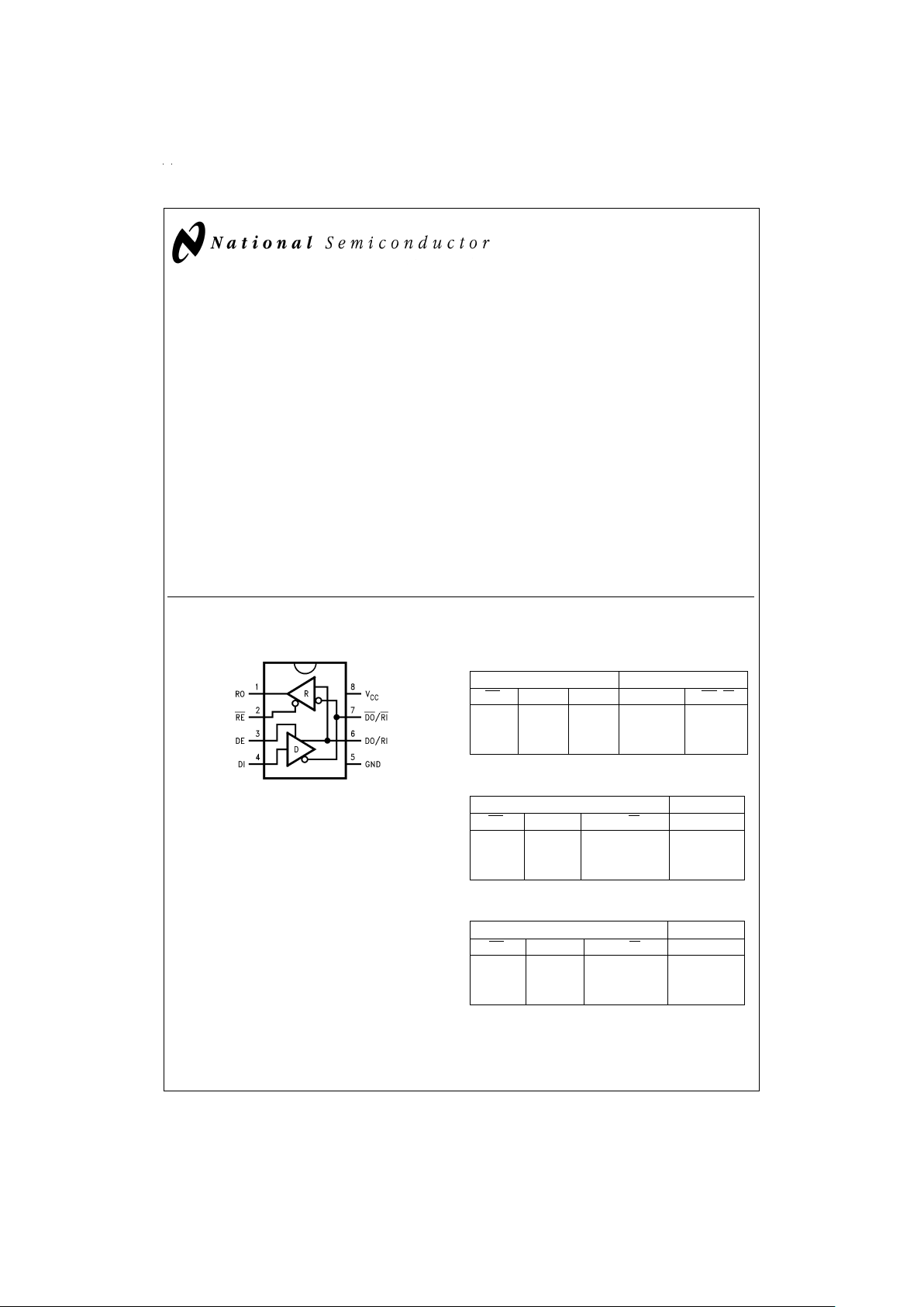
Connection and
Logic Diagram
Truth Tables
Driver
Inputs Outputs
RE
DE DI DO/RI DO /RI
XHH H L
XHL L H
XLX Z Z
Receiver
Inputs Output
RE
DE RI–RI RO
LL ≥0V H
LL≤−500 mV L
HX X Z
Receiver FAILSAFE
Inputs Output
RE
DE RI–RI RO
L L SHORTED H
L L OPEN H
HX X Z
TRI-STATE®is a registered trademark of National Semiconductor Corporation.
DS011383-1
Order Number DS36276M
See NS Package Number M08A
July 1998
DS36276 FAILSAFE Multipoint Transceiver
© 1999 National Semiconductor Corporation DS011383 www.national.com
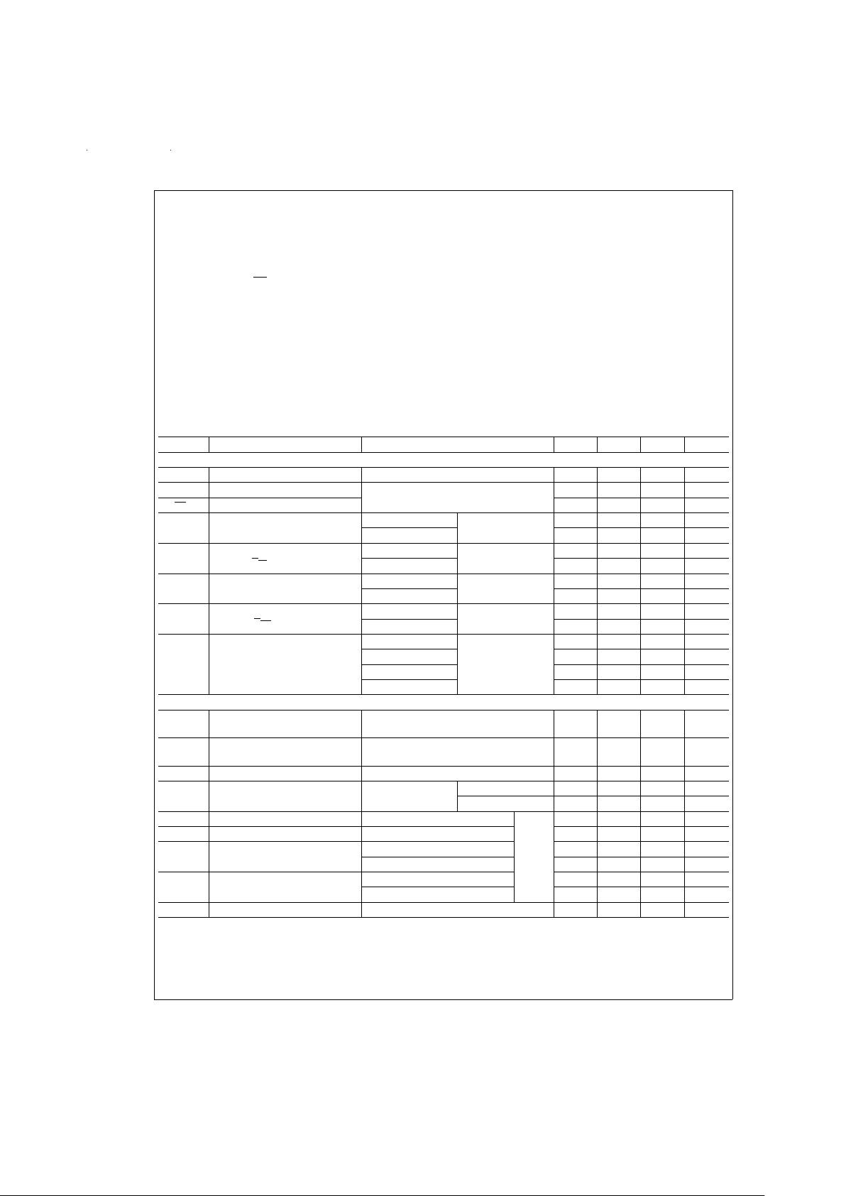
Absolute Maximum Ratings (Note 1)
If Military/Aerospace specified devices are required,
please contact the National Semiconductor Sales Office/
Distributors for availability and specifications.
Supply Voltage (V
CC
)7V
Input Voltage (DE, RE , and DI)
5.5V
Driver Output Voltage/
Receiver Input Voltage −10V to +15V
Receiver Output Voltage (RO) 5.5V
Maximum Package Power Dissipation
@
+25˚C
M Package
(derate 5.8 mW/˚C above
+25˚C) 726 mW
Storage Temperature Range −65˚C to +150˚C
Lead Temperature (Soldering 4
sec.) 260˚C
Max Junction Temperature 150˚C
ESD Rating (HBM, 1.5 kΩ, 100
pF) ≥ 6.0 kV
Recommended Operating
Conditions
Min Max Units
Supply Voltage, V
CC
4.75 5.25 V
Bus Voltage −7 +12 V
Operating Temperature (T
A
)
DS36276 0 +70 ˚C
Electrical Characteristics (Notes 2, 4)
Over recommended Supply Voltage and Operating Temperature ranges, unless otherwise specified.
Symbol Parameter Conditions Min Typ Max Units
DRIVER CHARACTERISTICS
V
OD
Differential Output Voltage IO= 0 mA (No Load) 1.5 4.8 6.0 V
V
oDO
Output Voltage IO= 0 mA (Output to GND) 0 6.0 V
V
oDO
Output Voltage 0 6.0 V
V
T1
Differential Output Voltage
(Termination Load)
RL=54Ω(485) (
Figure 1
) 1.5 2.0 5.0 V
R
L
= 100Ω (422) 2.0 2.3 5.0 V
∆V
T1
Balance of V
T1
|VT1|−|VT1|
RL=54Ω (Note 3) −0.2 0.07 +0.2 V
R
L
= 100Ω −0.2 0.07 +0.2 V
V
OS
Driver Common Mode
Output Voltage
RL=54Ω (
Figure 1
) 0 2.5 3.0 V
R
L
= 100Ω 0 2.3 3.0 V
∆V
OS
Balance of V
OS
|VOS|−|VOS|
RL=54Ω (Note 3) −0.2 0.08 +0.2 V
R
L
= 100Ω −0.2 0.08 +0.2 V
I
OSD
Driver Short-Circuit
Output Current
VO= +12V (
Figure 3
) 134 290 mA
V
O=VCC
140 mA
V
O
= 0V −140 mA
V
O
= −7V −180 −290 mA
RECEIVER CHARACTERISTICS
V
TH
Differential Input High
Threshold Voltage (Note 5)
VO=VOH,IO= −0.4 mA
−7V ≤ V
CM
≤ +12V
−0.18 0 V
V
TL
Differential Input Low
Threshold Voltage (Note 5)
VO=VOL,IO= 8.0 mA
−7V ≤ V
CM
≤ +12V
−0.5 −0.23 V
V
HST
Hysteresis (Note 6) VCM=0V 50 mV
I
IN
Line Input Current
(V
CC
= 4.75V, 5.25V, 0V)
Other Input = 0V
DE=VIH(Note 7)
V
I
= +12V 0.7 1.0 mA
V
I
= −7V −0.5 −0.8 mA
I
OSR
Short Circuit Current VO= 0V RO −5.0 −30 −85 mA
I
OZ
TRI-STATE®Leakage Current VO= 0.4 to 2.4V −20 +20 µA
V
OH
Output High Voltage
(
Figure 12
)
V
ID
= 0V, IOH= −0.4 mA 2.5 3.5 V
V
ID
= OPEN, IOH= −0.4 mA 2.5 3.5 V
V
OL
Output Low Voltage
(
Figure 12
)
V
ID
= −0.5V, IOL= +8 mA 0.25 0.6 V
V
ID
= −0.5V, IOL= +16 mA 0.35 0.7 V
R
IN
Input Resistance 12 19 kΩ
www.national.com 2
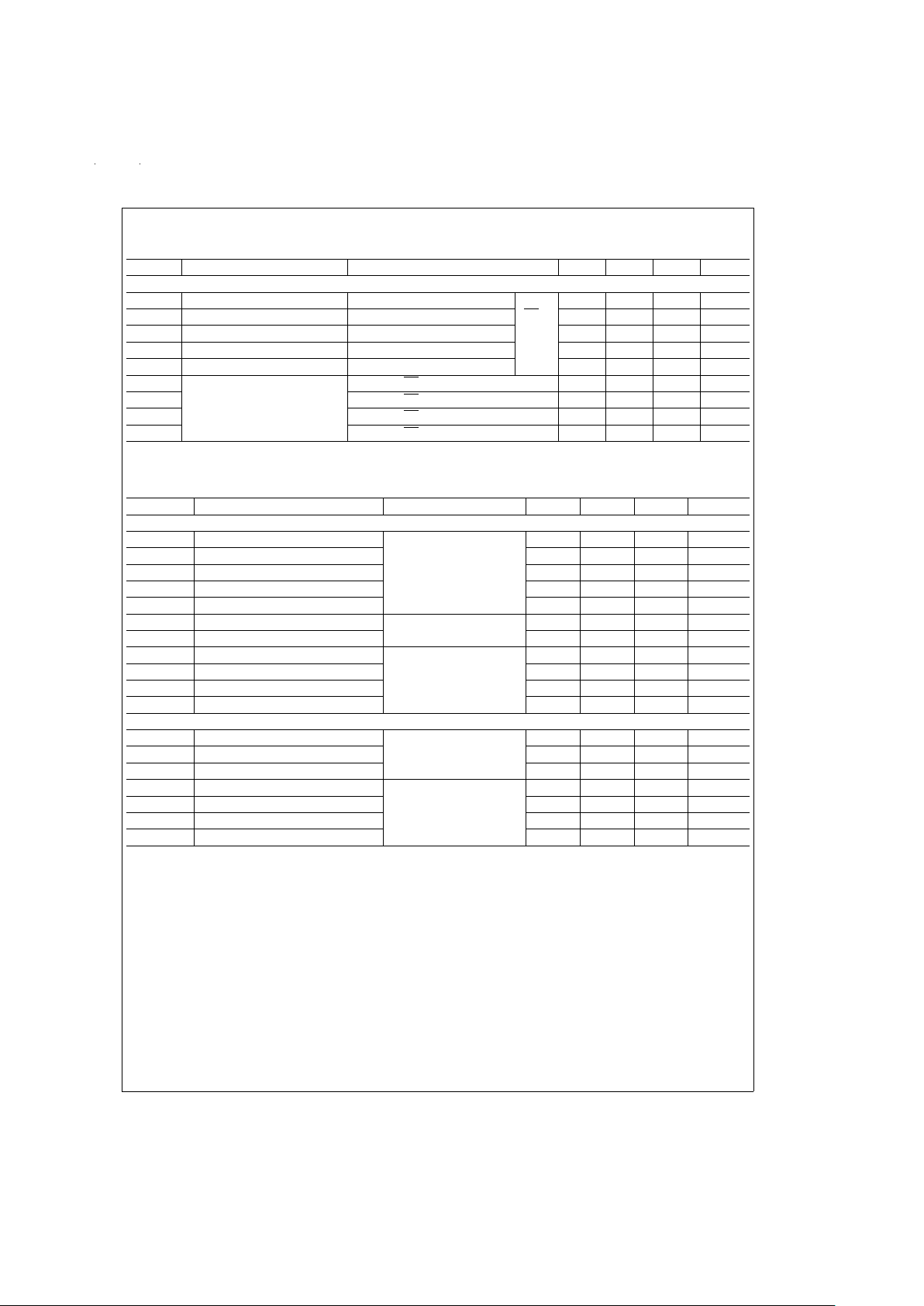
Electrical Characteristics (Notes 2, 4) (Continued)
Over recommended Supply Voltage and Operating Temperature ranges, unless otherwise specified.
Symbol Parameter Conditions Min Typ Max Units
DEVICE CHARACTERISTICS
V
IH
High Level Input Voltage DE,
RE,
or
DI
2.0 V
CC
V
V
IL
Low Level Input Voltage GND 0.8 V
I
IH
High Level Input Current VIH= 2.4V 20 µA
I
IL
Low Level Input Current VIL= 0.4V −100 µA
V
CL
Input Clamp Voltage ICL= −18 mA −0.75 −1.5 V
I
CC
Output Low Voltage
Supply Current
(No Load)
DE = 3V, RE = 0V, DI = 0V
42 60 mA
I
CCR
DE = 0V, RE = 0V, DI = 0V 28 45 mA
I
CCD
DE = 3V, RE = 3V, DI = 0V 43 60 mA
I
CCX
DE = 0V, RE = 3V, DI = 0V 31 50 mA
Switching Characteristics (Note 4)
Over recommended Supply Voltage and Operating Temperature ranges, unless otherwise specified.
Symbol Parameter Conditions Min Typ Max Units
DRIVER CHARACTERISTICS
t
PLHD
Diff. Prop. Delay Low to High RL=54Ω
C
L
=50pF
C
D
=50pF
(
Figures 4, 5
)
72160 ns
t
PHLD
Diff. Prop. Delay High to Low 7 19 60 ns
t
SKD
Diff. Skew (|t
PLHD–tPHLD
|) 2 10 ns
t
r
Diff. Rise Time 12 50 ns
t
f
Diff. Fall Time 12 50 ns
t
PLH
Prop. Delay Low to High RL=27Ω,CL=15pF
(
Figures 6, 7
)
22 45 ns
t
PHL
Prop. Delay High to Low 22 45 ns
t
PZH
Enable Time Z to High RL= 110Ω
C
L
=50pF
(
Figure 8–Figure 11
)
32 55 ns
t
PZL
Enable Time Z to Low 32 65 ns
t
PHZ
Disable Time High to Z 22 55 ns
t
PLZ
Disable Time Low to Z 16 55 ns
RECEIVER CHARACTERISTICS
t
PLH
Prop. Delay Low to High VID= −1.5V to +1.5V
C
L
=15pF
(
Figures 13, 14
)
15 40 70 ns
t
PHL
Prop. Delay High to Low 15 42 70 ns
t
SK
Skew (|t
PLH–tPHL
|) 2 15 ns
t
PZH
Enable Time Z to High CL=15pF
(
Figures 15, 16
)
15 50 ns
t
PZL
Enable Time Z to Low 17 50 ns
t
PHZ
Disable Time High to Z 24 50 ns
t
PLZ
Disable Time Low to Z 19 50 ns
Note 1: “Absolute Maximum Ratings”are those values beyond which the safety of the device cannot be guaranteed. They are not meant to imply that the devices
should be operated at these limits. The tables of “Electrical Characteristics” specify conditions for device operation.
Note 2: Current into devicepins is defined as positive. Current outof device pins is defined as negative.Allvoltagesare referenced to ground unless otherwise specified.
Note 3: ∆ |V
T1
| and ∆ |VOS| are changes in magnitude of VT1and VOS, respectively, that occur when the input changes state.
Note 4: All typicals are given for V
CC
= 5.0V and TA= +25˚C.
Note 5: Threshold parameter limits specified as an algebraic value rather than by magnitude.
Note 6: Hysteresis defined as V
HST=VTH−VTL
.
Note 7: I
IN
includes the receiver input current and driver TRI-STATE leakage current.
www.national.com3
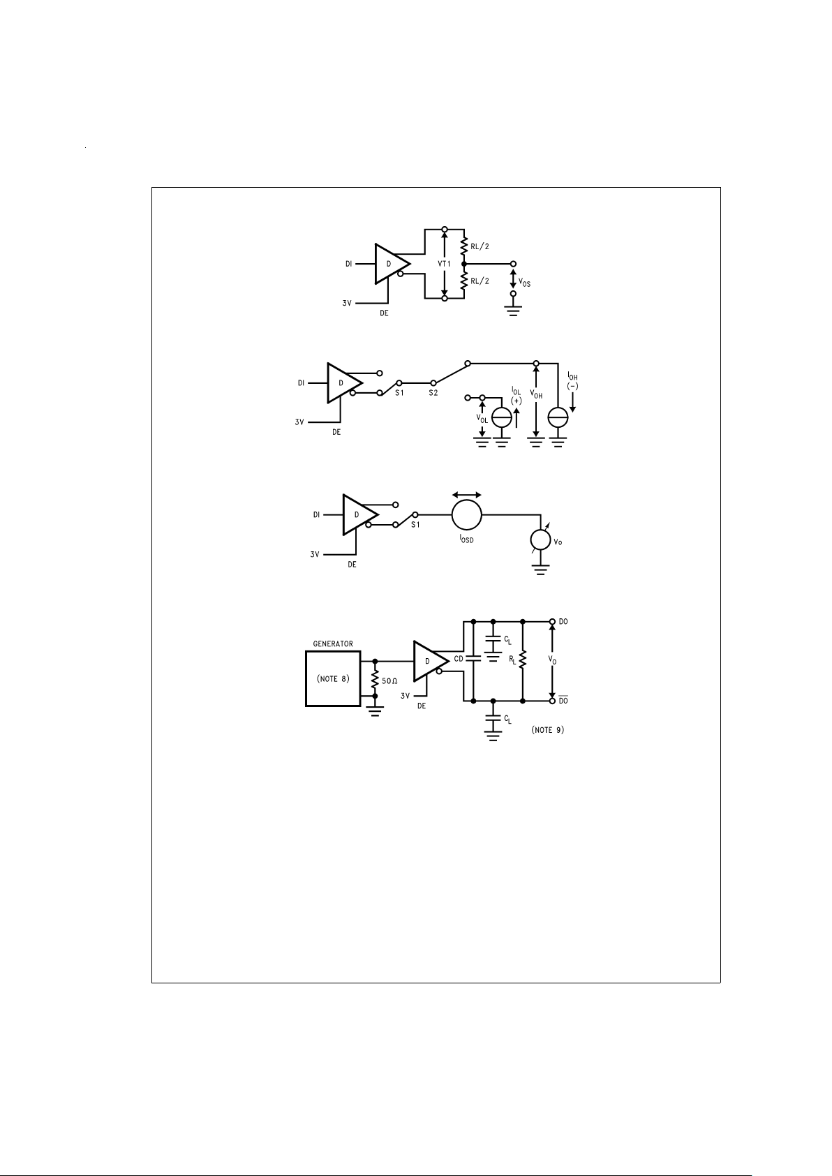
Parameter Measurement Information
DS011383-2
FIGURE 1. Driver VT1and VOSTest Circuit
DS011383-3
FIGURE 2. Driver VOHand VOLTest Circuit
DS011383-4
FIGURE 3. Driver Short Circuit Test Circuit
DS011383-5
FIGURE 4. Driver Differential Propagation Delay and Transition Time Test Circuit
www.national.com 4
 Loading...