NSC CD4060BMW-MIL, CD4060BMJ-MIL Datasheet

TL/F/5953
CD4020BM/BC 14-Stage Ripple Carry Binary Counters/CD4040BM/BC 12-Stage
Ripple Carry Binary Counters CD4060BM/BC 14-Stage Ripple Carry Binary Counters
February 1988
CD4020BM/CD4020BC
14-Stage Ripple Carry Binary Counters
CD4040BM/CD4040BC
12-Stage Ripple Carry Binary Counters
CD4060BM/CD4060BC
14-Stage Ripple Carry Binary Counters
General Description
The CD4020BM/CD4020BC, CD4060BM/CD4060BC are
14-stage ripple carry binary counters, and the CD4040BM/
CD4040BC is a 12-stage ripple carry binary counter. The
counters are advanced one count on the negative transition
of each clock pulse. The counters are reset to the zero state
by a logical ‘‘1’’ at the reset input independent of clock.
Features
Y
Wide supply voltage range 1.0V to 15V
Y
High noise immunity 0.45 VDD(typ.)
Y
Low power TTL Fan out of 2 driving 74L
compatibility or 1 driving 74LS
Y
Medium speed operation 8 MHz typ. at V
DD
e
10V
Y
Schmitt trigger clock input
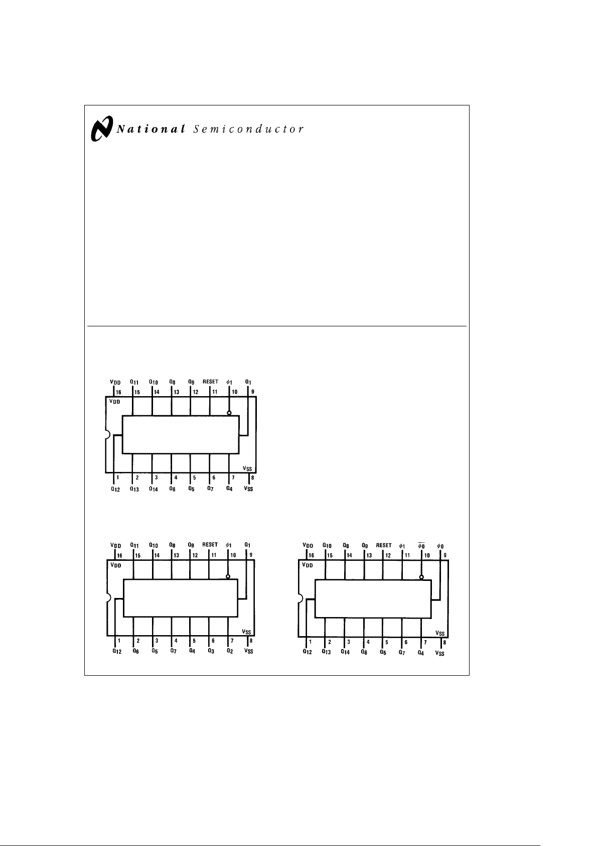
Connection Diagrams
Dual-In-Line Package
CD4020BM/CD4020BC
TL/F/5953– 1
Top View
Order Number CD4020B, CD4040B or CD4060B
Dual-In-Line Package
CD4040BM/CD4040BC
TL/F/5953– 2
Top View
Dual-In-Line Package
CD4060BM/CD4060BC
TL/F/5953– 3
Top View
C
1995 National Semiconductor Corporation RRD-B30M105/Printed in U. S. A.

Absolute Maximum Ratings (Notes 1 and 2)
If Military/Aerospace specified devices are required,
please contact the National Semiconductor Sales
Office/Distributors for availability and specifications.
Supply Voltage (V
DD
)
b
0.5V toa18V
Input Voltage (VIN)
b
0.5V to V
DD
a
0.5V
Storage Temperature Range (T
S
)
b
65§Ctoa150§C
Package Dissipation (PD)
Dual-In-Line 700 mW
Small Outline 500 mW
Lead Temperature (T
L
)
(Soldering, 10 seconds) 260
§
C
Recommended Operating
Conditions
Supply Voltage (VDD)
a
3V toa15V
Input Voltage (VIN) 0VtoV
DD
Operating Temperature Range (TA)
CD40XXBM
b
55§Ctoa125§C
CD40XXBC
b
40§Ctoa85§C
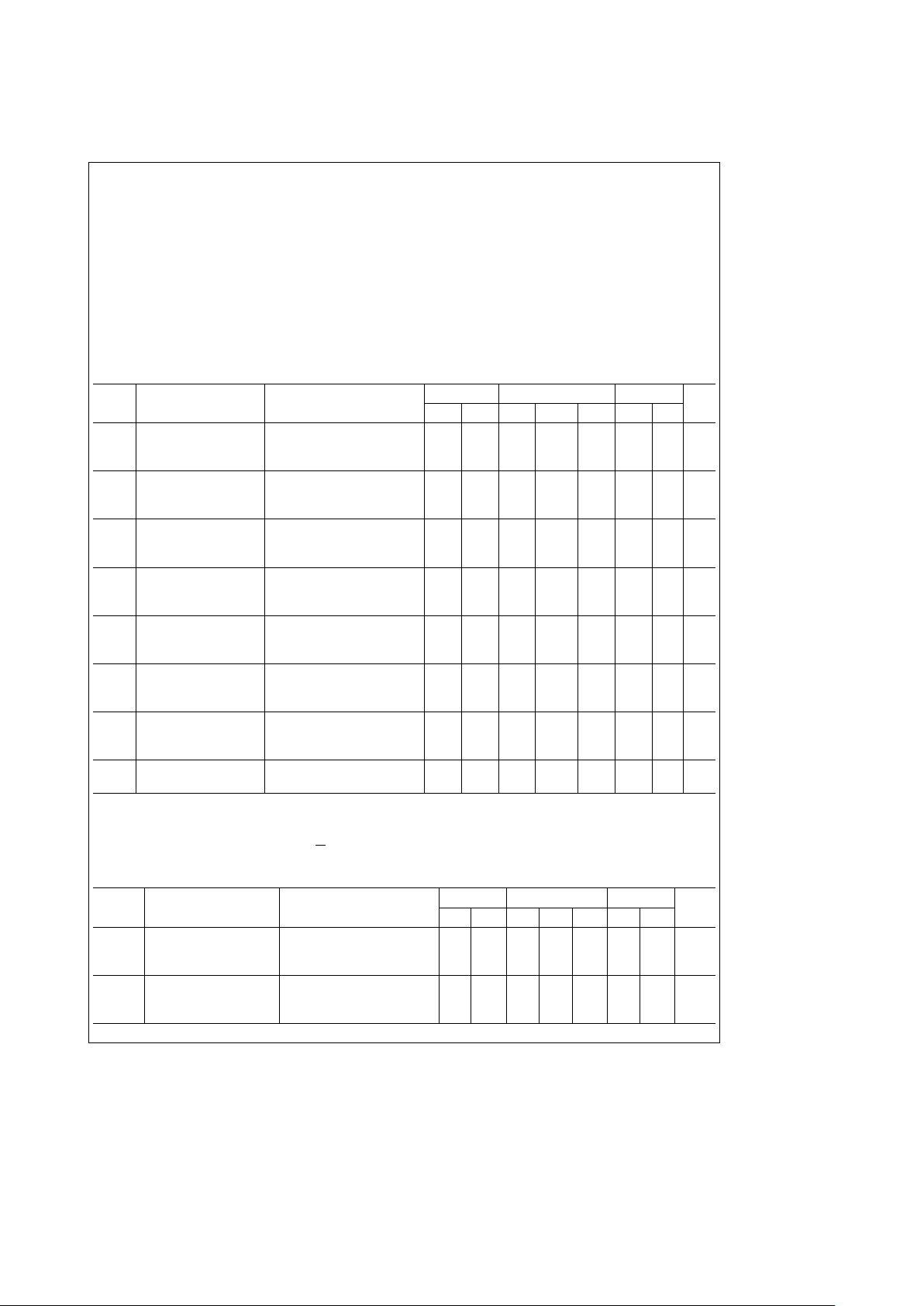
DC Electrical Characteristics CD40XXBM (Note 2)
Symbol Parameter Conditions
b
55§C
a
25§C
a
125§C
Units
Min Max Min Typ Max Min Max
I
DD
Quiescent Device Current V
DD
e
5V, V
IN
e
VDDor V
SS
5 5 150 mA
V
DD
e
10V, V
IN
e
VDDor V
SS
10 10 300 mA
V
DD
e
15V, V
IN
e
VDDor V
SS
20 20 600 mA
V
OL
Low Level Output Voltage V
DD
e
5V 0.05 0 0.05 0.05 V
V
DD
e
10V 0.05 0 0.05 0.05 V
V
DD
e
15V 0.05 0 0.05 0.05 V
V
OH
High Level Output Voltage V
DD
e
5V 4.95 4.95 5 4.95 V
V
DD
e
10V 9.95 9.95 10 9.95 V
V
DD
e
15V 14.95 14.95 15 14.95 V
V
IL
Low Level Input Voltage V
DD
e
5V, V
O
e
0.5V or 4.5V 1.5 2 1.5 1.5 V
V
DD
e
10V, V
O
e
1.0V or 9.0V 3.0 4 3.0 3.0 V
V
DD
e
15V, V
O
e
1.5V or 13.5V 4.0 6 4.0 4.0 V
V
IH
High Level Input Voltage V
DD
e
5V, V
O
e
0.5V or 4.5V 3.5 3.5 3 3.5 V
V
DD
e
10V, V
O
e
1.0V or 9.0V 7.0 7.0 6 7.0 V
V
DD
e
15V, V
O
e
1.5V or 13.5V 11.0 11.0 9 11.0 V
I
OL
Low Level Output Current V
DD
e
5V, V
O
e
0.4V 0.64 0.51 0.88 0.36 mA
(See Note 3) V
DD
e
10V, V
O
e
0.5V 1.6 1.3 2.25 0.9 mA
V
DD
e
15V, V
O
e
1.5V 4.2 3.4 8.8 2.4 mA
I
OH
High Level Output Current V
DD
e
5V, V
O
e
4.6V
b
0.64
b
0.51b0.88
b
0.36 mA
(See Note 3) V
DD
e
10V, V
O
e
9.5V
b
1.6
b
1.3b2.25
b
0.9 mA
V
DD
e
15V, V
O
e
13.5V
b
4.2
b
3.4b8.8
b
2.4 mA
I
IN
Input Current V
DD
e
15V, V
IN
e
0V
b
0.10
b
10
b
5
b
0.10
b
1.0 mA
V
DD
e
15V, V
IN
e
15V 0.10 10
b
5
0.10 1.0 mA
Note 1: ‘‘Absolute Maximum Ratings’’ are those values beyond which the safety of the device cannot be guaranteed. They are not meant to imply that the devices
should be operated at these limits. The tables of ‘‘Recommended Operating Conditions’’ and ‘‘Electrical Characteristics’’ provide conditions for actual device
operation.
Note 2: V
SS
e
0V unless otherwise specified.
Note 3: Data does not apply to oscillator points w
0
and w
0
of CD4060BM/CD4060BC. IOHand IOLare tested one output at a time.
DC Electrical Characteristics 40XXBC (Note 2)
Symbol Parameter Conditions
b
40§C
a
25§C
a
85§C
Units
Min Max Min Typ Max Min Max
I
DD
Quiescent Device Current V
DD
e
5V, V
IN
e
VDDor V
SS
20 20 150 mA
V
DD
e
10V, V
IN
e
VDDor V
SS
40 40 300 mA
V
DD
e
15V, V
IN
e
VDDor V
SS
80 80 600 mA
V
OL
Low Level Output Voltage V
DD
e
5V 0.05 0 0.05 0.05 V
V
DD
e
10V 0.05 0 0.05 0.05 V
V
DD
e
15V 0.05 0 0.05 0.05 V
2
 Loading...