NSC CD4053BMW-883, CD4053BMJ-883 Datasheet

TL/F/5662
CD4051BM/CD4051BC, CD4052BM/CD4052BC, CD4053BM/CD4053BC
Analog Multiplexer/Demultiplexers
October 1989
CD4051BM/CD4051BC Single 8-Channel Analog
Multiplexer/Demultiplexer
CD4052BM/CD4052BC Dual 4-Channel Analog
Multiplexer/Demultiplexer
CD4053BM/CD4053BC Triple 2-Channel Analog
Multiplexer/Demultiplexer
General Description
These analog multiplexers/demultiplexers are digitally controlled analog switches having low ‘‘ON’’ impedance and
very low ‘‘OFF’’ leakage currents. Control of analog signals
up to 15V
p-p
can be achieved by digital signal amplitudes of
3–15V. For example, if V
DD
e
5V, V
SS
e
0V and V
EE
eb
5V,
analog signals from
b
5V toa5V can be controlled by digital inputs of 0 – 5V. The multiplexer circuits dissipate extremely low quiescent power over the full V
DD
b
VSSand
V
DD
b
VEEsupply voltage ranges, independent of the logic
state of the control signals. When a logical ‘‘1’’ is present at
the inhibit input terminal all channels are ‘‘OFF’’.
CD4051BM/CD4051BC is a single 8-channel multiplexer
having three binary control inputs. A, B, and C, and an inhibit
input. The three binary signals select 1 of 8 channels to be
turned ‘‘ON’’ and connect the input to the output.
CD4052BM/CD4052BC is a differential 4-channel multiplexer having two binary control inputs, A and B, and an inhibit
input. The two binary input signals select 1 or 4 pairs of
channels to be turned on and connect the differential analog inputs to the differential outputs.
CD4053BM/CD4053BC is a triple 2-channel multiplexer
having three separate digital control inputs, A, B, and C, and
an inhibit input. Each control input selects one of a pair of
channels which are connected in a single-pole double-throw
configuration.
Features
Y
Wide range of digital and analog signal levels: digital
3–15V, analog to 15V
p-p
Y
Low ‘‘ON’’ resistance: 80X (typ.) over entire 15V
p-p
sig-
nal-input range for V
DD
b
V
EE
e
15V
Y
High ‘‘OFF’’ resistance: channel leakage ofg10 pA
(typ.) at V
DD
b
V
EE
e
10V
Y
Logic level conversion for digital addressing signals of
3–15V (V
DD
b
V
SS
e
3–15V) to switch analog signals to
15 V
p-p(VDD
b
V
EE
e
15V)
Y
Matched switch characteristics: DR
ON
e
5X (typ.) for
V
DD
b
V
EE
e
15V
Y
Very low quiescent power dissipation under all digitalcontrol input and supply conditions: 1 mW (typ.) at
V
DD
b
V
SS
e
V
DD
b
V
EE
e
10V
Y
Binary address decoding on chip
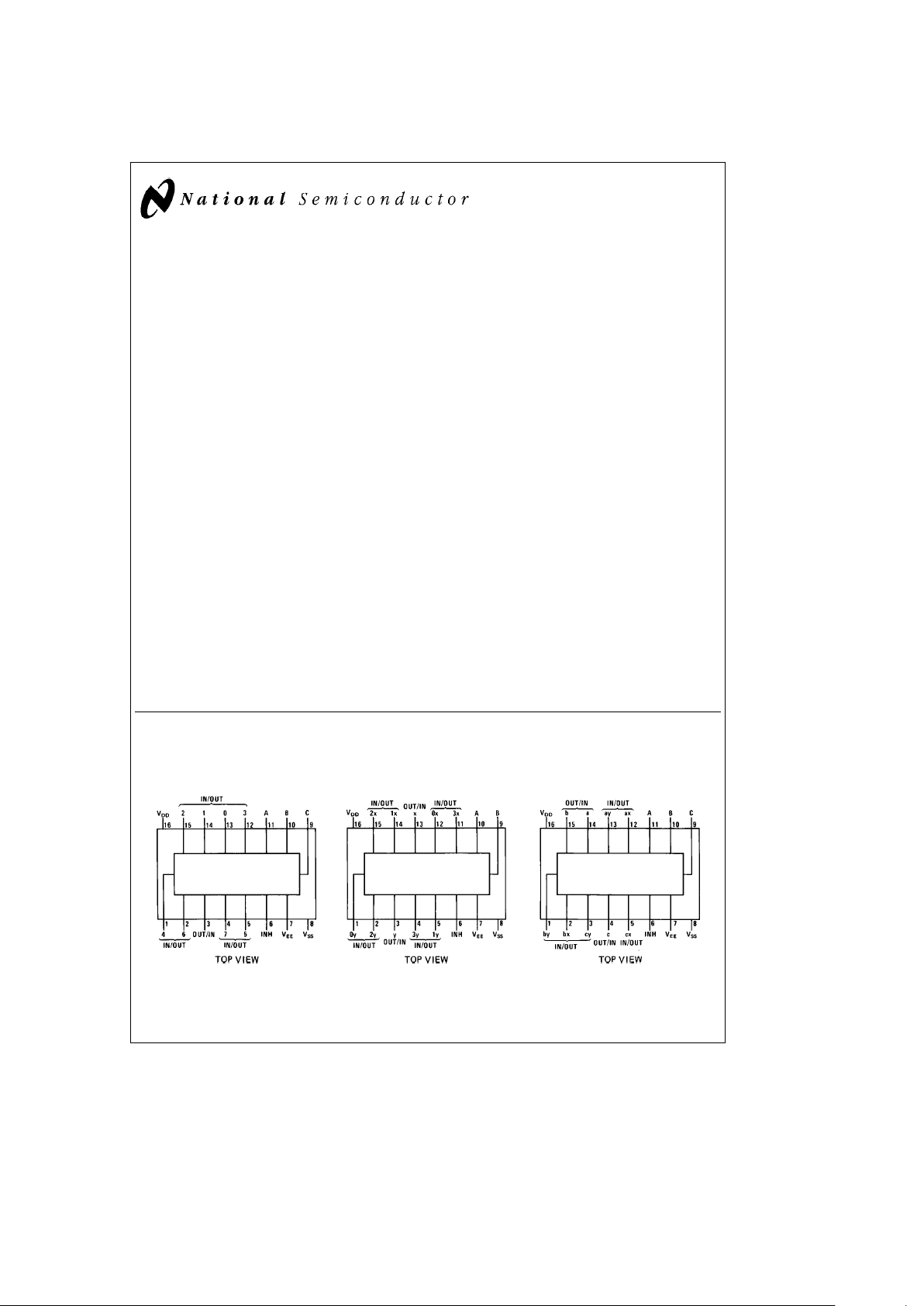
Connection Diagrams
Dual-In-Line Packages
CD4051BM/CD4051BC CD4052BM/CD4052BC CD4053BM/CD4053BC
TL/F/5662– 1
Order Number CD4051B, CD4052B, or CD4053B
C
1995 National Semiconductor Corporation RRD-B30M105/Printed in U. S. A.

Absolute Maximum Ratings
If Military/Aerospace specified devices are required,
please contact the National Semiconductor Sales
Office/Distributors for availability and specifications.
DC Supply Voltage (V
DD
)
b
0.5 VDCtoa18 V
DC
Input Voltage (VIN)
b
0.5 VDCto V
DD
a
0.5 V
DC
Storage Temperature Range (TS)
b
65§Ctoa150§C
Power Dissipation (P
D
)
Dual-In-Line 700 mW
Small Outline 500 mW
Lead Temp. (T
L
) (soldering, 10 sec.) 260§C
Recommended Operating
Conditions
DC Supply Voltage (VDD)
a
5VDCtoa15 V
DC
Input Voltage (VIN) 0VtoVDDV
DC
Operating Temperature Range (TA)
4051BM/4052BM/4053BM
b
55§Ctoa125§C
4051BC/4052BC/4053BC
b
40§Ctoa85§C
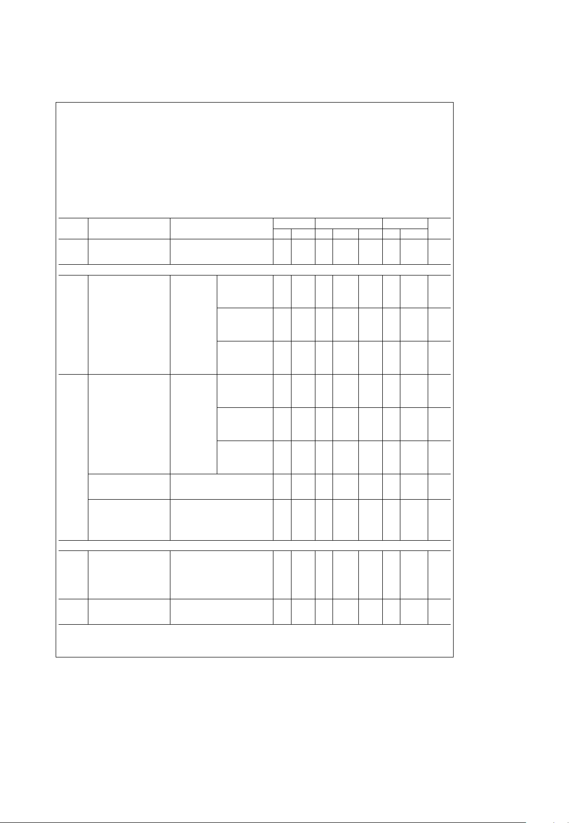
DC Electrical Characteristics (Note 2)
Symbol Parameter Conditions
b
55§C
a
25
§
a
125§C
Units
Min Max Min Typ Max Min Max
I
DD
Quiescent Device Current V
DD
e
5V 5 5 150 mA
V
DD
e
10V 10 10 300 mA
V
DD
e
15V 20 20 600 mA
Signal Inputs (VIS) and Outputs (VOS)
R
ON
‘‘ON’’ Resistance (Peak R
L
e
10 kX V
DD
e
2.5V,
for V
EE
s
V
IS
s
VDD) (any channel V
EE
eb
2.5V
800 270 1050 1300 X
selected) or V
DD
e
5V,
V
EE
e
0V
V
DD
e
5V
V
EE
eb
5V
310 120 400 550 X
or V
DD
e
10V,
V
EE
e
0V
V
DD
e
7.5V,
V
EE
eb
7.5V
200 80 240 320 X
or V
DD
e
15V,
V
EE
e
0V
DR
ON
D‘‘ON’’ Resistance R
L
e
10 kX V
DD
e
2.5V,
Between Any Two (any channel V
EE
eb
2.5V
10 X
Channels selected) or V
DD
e
5V,
V
EE
e
0V
V
DD
e
5V,
V
EE
eb
5V
10 X
or V
DD
e
10V,
V
EE
e
0V
V
DD
e
7.5V,
V
EE
eb
7.5V
5 X
or V
DD
e
15V,
V
EE
e
0V
‘‘OFF’’ Channel Leakage V
DD
e
7.5V, V
EE
eb
7.5V
Current, any channel O/I
e
g
7.5V, I/Oe0V
g
50
g
0.01g50
g
500 nA
‘‘OFF’’
‘‘OFF’’ Channel Leakage Inhibite7.5V CD4051
g
200
g
0.08g200
g
2000 nA
Current, all channels V
DD
e
7.5V,
‘‘OFF’’ (Common V
EE
eb
7.5V, CD4052
g
200
g
0.04g200
g
2000 nA
OUT/IN) O/I
e
0V,
I/O
e
g
7.5V CD4053
g
200
g
0.02g200
g
2000 nA
Control Inputs A, B, C and Inhibit
V
IL
Low Level Input Voltage V
EE
e
VSSR
L
e
1kXto V
SS
I
IS
k
2 mA on all OFF channels
V
IS
e
VDDthru 1 kX
V
DD
e
5V 1.5 1.5 1.5 V
V
DD
e
10V 3.0 3.0 3.0 V
V
DD
e
15V 4.0 4.0 4.0 V
V
IH
High Level Input Voltage V
DD
e
5 3.5 3.5 3.5 V
V
DD
e
10 7 7 7 V
V
DD
e
15 11 11 11 V
Note 1: ‘‘Absolute Maximum Ratings’’ are those values beyond which the safety of the device cannot be guaranteed. Except for ‘‘Operating Temperature Range’’
they are not meant to imply that the devices should be operated at these limits. The table of ‘‘Electrical Characteristics’’ provides conditions for actual device
operation.
Note 2: All voltages measured with respect to V
SS
unless otherwise specified.
2

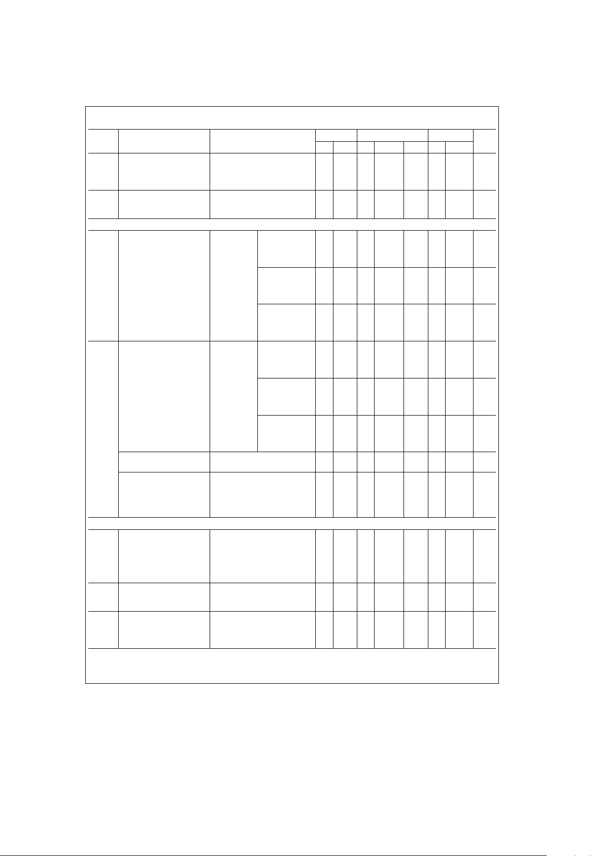
DC Electrical Characteristics (Note 2) (Continued)
Symbol Parameter Conditions
b
40§C
a
25§C
a
85§C
Units
Min Max Min Typ Max Min Max
I
IN
Input Current V
DD
e
15V, V
EE
e
0V
b
0.1
b
10
b
5
b
0.1
b
1.0 mA
V
IN
e
0V
V
DD
e
15V, V
EE
e
0V
0.1 10
b
5
0.1 1.0 mA
V
IN
e
15V
I
DD
Quiescent Device Current V
DD
e
5V 20 20 150 mA
V
DD
e
10V 40 40 300 mA
V
DD
e
15V 80 80 600 mA
Signal Inputs (VIS) and Outputs (VOS)
R
ON
‘‘ON’’ Resistance (Peak R
L
e
10 kX V
DD
e
2.5V,
for V
EE
s
V
IS
s
VDD) (any channel V
EE
eb
2.5V
850 270 1050 1200 X
selected) or V
DD
e
5V,
V
EE
e
0V
V
DD
e
5V,
V
EE
eb
5V
330 120 400 520 X
or V
DD
e
10V,
V
EE
e
0V
V
DD
e
7.5V,
V
EE
eb
7.5V
210 80 240 300 X
or V
DD
e
15V,
V
EE
e
0V
DROND‘‘ON’’ Resistance R
L
e
10 kX V
DD
e
2.5V,
Between Any Two (any channel V
EE
eb
2.5V
10 X
Channels selected) or V
DD
e
5V,
V
EE
e
0V
V
DD
e
5V
V
EE
eb
5V
10 X
or V
DD
e
10V,
V
EE
e
0V
V
DD
e
7.5V,
V
EE
eb
7.5V
5 X
or V
DD
e
15V,
V
EE
e
0V
‘‘OFF’’ Channel Leakage V
DD
e
7.5V, V
EE
eb
7.5V
Current, any channel ‘‘OFF’’ O/I
e
g
7.5V, I/Oe0V
g
50
g
0.01g50
g
500 nA
‘‘OFF’’ Channel Leakage Inhibite7.5V CD4051
g
200
g
0.08g200
g
2000 nA
Current, all channels V
DD
e
7.5V,
‘‘OFF’’ (Common V
EE
eb
7.5V, CD4052
g
200
g
0.04g200
g
2000 nA
OUT/IN) O/I
e
0V
I/O
e
g
7.5V CD4053
g
200
g
0.02g200
g
2000 nA
Control Inputs A, B, C and Inhibit
V
IL
Low Level Input Voltage V
EE
e
VSSR
L
e
1kXto V
SS
I
IS
k
2 mA on all OFF Channels
V
IS
e
VDDthru 1 kX
V
DD
e
5V 1.5 1.5 1.5 V
V
DD
e
10V 3.0 3.0 3.0 V
V
DD
e
15V 4.0 4.0 4.0 V
V
IH
High Level Input Voltage V
DD
e
5 3.5 3.5 3.5 V
V
DD
e
10 7 7 7 V
V
DD
e
15 11 11 11 V
I
IN
Input Current V
DD
e
15V, V
EE
e
0V
b
0.1
b
10
b
5
b
0.1
b
1.0 mA
V
IN
e
0V
V
DD
e
15V, V
EE
e
0V
0.1 10
b
5
0.1 1.0 mA
V
IN
e
15V
Note 1: ‘‘Absolute Maximum Ratings’’ are those values beyond which the safety of the device cannot be guaranteed. Except for ‘‘Operating Temperature Range’’
they are not meant to imply that the devices should be operated at these limits. The table of ‘‘Electrical Characteristics’’ provides conditions for actual device
operation.
Note 2: All voltages measured with respect to V
SS
unless otherwise specified.
3
 Loading...