NSC CD4050BMW-883 Datasheet

TL/F/5971
CD4049UBM/CD4049UBC Hex Inverting Buffer
CD4050BM/CD4050BC Hex Non-Inverting Buffer
March 1988
CD4049UBM/CD4049UBC Hex Inverting Buffer
CD4050BM/CD4050BC Hex Non-Inverting Buffer
General Description
These hex buffers are monolithic complementary MOS
(CMOS) integrated circuits constructed with N- and P-channel enhancement mode transistors. These devices feature
logic level conversion using only one supply voltage (V
DD
).
The input signal high level (V
IH
) can exceed the VDDsupply
voltage when these devices are used for logic level conversions. These devices are intended for use as hex buffers,
CMOS to DTL/TTL converters, or as CMOS current drivers,
and at V
DD
e
5.0V, they can drive directly two DTL/TTL
loads over the full operating temperature range.
Features
Y
Wide supply voltage range 3.0V to 15V
Y
Direct drive to 2 TTL loads at 5.0V over full temperature range
Y
High source and sink current capability
Y
Special input protection permits input voltages greater
than V
DD
Applications
Y
CMOS hex inverter/buffer
Y
CMOS to DTL/TTL hex converter
Y
CMOS current ‘‘sink’’ or ‘‘source’’ driver
Y
CMOS high-to-low logic level converter
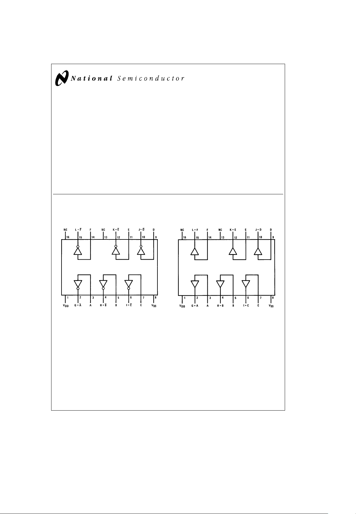
Connection Diagrams
CD4049UBM/CD4049UBC
Dual-In-Line Package
TL/F/5971– 1
Top View
Order Number CD4049UB or CD4049B
CD4050BM/CD4050BC
Dual-In-Line Package
TL/F/5971– 2
Top View
Order Number CD4050UB or CD4050B
C
1995 National Semiconductor Corporation RRD-B30M105/Printed in U. S. A.

Absolute Maximum Ratings (Notes1&2)
If Military/Aerospace specified devices are required,
please contact the National Semiconductor Sales
Office/Distributors for availability and specifications.
Supply Voltage (V
DD
)
b
0.5V toa18V
Input Voltage (VIN)
b
0.5V toa18V
Voltage at Any Output Pin (V
OUT
)
b
0.5V to V
DD
a
0.5V
Storage Temperature Range (TS)
b
65§Ctoa150§C
Power Dissipation (PD)
Dual-In-Line 700 mW
Small Outline 500 mW
Lead Temperature (T
L
)
(Soldering, 10 seconds) 260
§
C
Recommended Operating
Conditions
(Note 2)
Supply Voltage (VDD) 3Vto15V
Input Voltage (VIN) 0Vto15V
Voltage at Any Output Pin (V
OUT
) 0 to V
DD
Operating Temperature Range (TA)
CD4049UBM, CD4050BM
b
55§Ctoa125§C
CD4049UBC, CD4050BC
b
40§Ctoa85§C
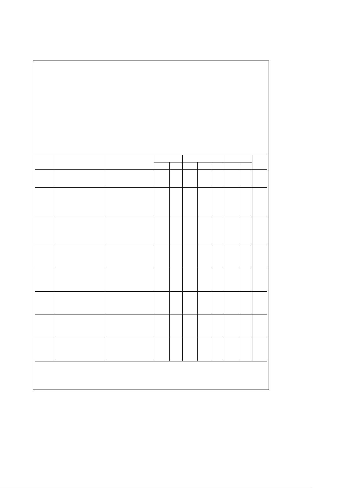
DC Electrical Characteristics CD4049M/CD4050BM (Note 2)
Symbol Parameter Conditions
b
55§C
a
25§C
a
125§C
Units
Min Max Min Typ Max Min Max
I
DD
Quiescent Device Current V
DD
e
5V 1.0 0.01 1.0 30 mA
V
DD
e
10V 2.0 0.01 2.0 60 mA
V
DD
e
15V 4.0 0.03 4.0 120 mA
V
OL
Low Level Output Voltage V
IH
e
VDD,V
IL
e
0V,
l
I
O
l
k
1 mA
V
DD
e
5V 0.05 0 0.05 0.05 V
V
DD
e
10V 0.05 0 0.05 0.05 V
V
DD
e
15V 0.05 0 0.05 0.05 V
V
OH
High Level Output Voltage V
IH
e
VDD,V
IL
e
0V,
l
I
O
l
k
1 mA
V
DD
e
5V 4.95 4.95 5 4.95 V
V
DD
e
10V 9.95 9.95 10 9.95 V
V
DD
e
15V 14.95 14.95 15 14.95 V
V
IL
Low Level Input VoltagelI
O
l
k
1 mA
(CD4050BM Only) V
DD
e
5V, V
O
e
0.5V 1.5 2.25 1.5 1.5 V
V
DD
e
10V, V
O
e
1V 3.0 4.5 3.0 3.0 V
V
DD
e
15V, V
O
e
1.5V 4.0 6.75 4.0 4.0 V
V
IL
Low Level Input VoltagelI
O
l
k
1 mA
(CD4049UBM Only) V
DD
e
5V, V
O
e
4.5V 1.0 1.5 1.0 1.0 V
V
DD
e
10V, V
O
e
9V 2.0 2.5 2.0 2.0 V
V
DD
e
15V, V
O
e
13.5V 3.0 3.5 3.0 3.0 V
V
IH
High Level Input VoltagelI
O
l
k
1 mA
(CD4050BM Only) V
DD
e
5V, V
O
e
4.5V 3.5 3.5 2.75 3.5 V
V
DD
e
10V, V
O
e
9V 7.0 7.0 5.5 7.0 V
V
DD
e
15V, V
O
e
13.5V 11.0 11.0 8.25 11.0 V
V
IH
High Level Input VoltagelI
O
l
k
1 mA
(CD4049UBM Only) V
DD
e
5V, V
O
e
0.5V 4.0 4.0 3.5 4.0 V
V
DD
e
10V, V
O
e
1V 8.0 8.0 7.5 8.0 V
V
DD
e
15V, V
O
e
1.5V 12.0 12.0 11.5 12.0 V
I
OL
Low Level Output Current V
IH
e
VDD,V
IL
e
0V
(Note 3) V
DD
e
5V, V
O
e
0.4V 5.6 4.6 5 3.2 mA
V
DD
e
10V, V
O
e
0.5V 12 9.8 12 6.8 mA
V
DD
e
15V, V
O
e
1.5V 35 29 40 20 mA
Note 1: ‘‘Absolute Maximum Ratings’’ are those values beyond which the safety of the device cannot be guaranteed; they are not meant to imply that the devices
should be operated at these limits. The table of ‘‘Recommended Operating Conditions’’ and ‘‘Electrical Characteristics’’ provides conditions for actual device
operation.
Note 2: V
SS
e
0V unless otherwise specified.
Note 3: These are
peak
output current capabilities. Continuous output current is rated at 12 mA maximum. The output current should not be allowed to exceed this
value for extended periods of time. I
OL
and IOHare tested one output at a time.
2
 Loading...