

Datasheet ADC0858CMJ-QML, ADC0858CIVX, ADC0858CIN, ADC0858BIVX, ADC0858BIV Datasheet (NSC)
...
TL/H/11021
ADC0851 and ADC0858 8-Bit Analog Data Acquisition and Monitoring Systems
January 1995
ADC0851 and ADC0858 8-Bit Analog Data
Acquisition and Monitoring Systems
General Description
The ADC0851 and ADC0858 are 2 and 8 input analog data
acquisition systems. They can function as conventional multiple input A/D converters, automatic scanning A/D converters or programmable analog ‘‘watchdog’’ systems. In
‘‘watchdog’’ mode they monitor analog inputs and determine whether these inputs are inside or outside user programmed window limits. This monitoring process takes
place independent of the host processor. When any input
falls outside of its programmed window limits, an interrupt is
automatically generated which flags the processor; the chip
can then be interrogated as to exactly which channels
crossed which limits.
The advantage of this approach is that its frees the processor from having to frequently monitor analog variables. It
can consequently save having to insert many A/D subroutine calls throughout real time application code. In control
systems where many variables are continually being monitored this can significantly free up the processor, especially
if the variables are DC or slow varying signals.
The Auto A/D conversion feature allows the device to scan
through selected input channels, performing an A/D conversion on each channel without the need to select a new
channel after each conversion.
Applications
Y
Instrumentation monitoring and process control
Y
Digitizing automotive sensor signals
Y
Embedded diagnostics
Key Specifications
Y
Resolution 8 Bits
Y
Total error
g
(/2 LSB org1 LSB
Y
Low power 50 mW
Y
Conversion time 18 ms/Channel
Y
Limit comparison time 2 ms/Limit
Features
Y
Watchdog operation signals processor when any
channel is outside user programmed window limits
Y
Frees microprocessor from continually monitoring
analog signals and simplifies applications software
Y
2 (ADC0851) or 8 (ADC0858) analog input channels
Y
Single ended or differential input pairs
Y
COM input for DC offsetting of input voltage
Y
4 (ADC0851) and 16 (ADC0858), 8-bit programmable
limits
Y
NSC MICROWIRETMinterface
Y
Power fail detection
Y
Auto A/D conversion feature
Y
Single 5V supply
Y
Window limits are user programmable via serial interface
Simplified Block Diagram
TL/H/11021– 22
FIGURE 1
TRI-STATEÉis a registered trademark of National Semiconductor Corporation.
MICROWIRE
TM
is a trademark of National Semiconductor Corporation.
C
1995 National Semiconductor Corporation RRD-B30M75/Printed in U. S. A.
Connection Diagrams
ADC0851
2-Channel MUX
Dual-In-Line Package
TL/H/11021– 1
Top View
ADC0858
8-Channel MUX
Dual-In-Line Package
TL/H/11021– 2
Top View
ADC0851 PLCC Package
TL/H/11021– 3
Top View
ADC0858 PLCC Package
TL/H/11021– 4
Top View
Ordering Information
Industrial
Package
(
b
40§CsT
A
s
a
85§C)
ADC0851BIN, N16E, 16-Pin
ADC0851CIN Plastic DIP
ADC0858BIN, N20A, 20-Pin
ADC0858CIN Plastic DIP
ADC0851BIV, V20A, 20-Lead
ADC0851CIV PLCC
ADC0858BIV, V20A, 20-Lead
ADC0858CIV PLCC
Military
Package
(
b
55§CsT
A
s
a
125§C)
ADC0851CMJ/883 J16A, 16-Pin
Ceramic DIP
ADC0858CMJ/883 J20A, 20-Pin
Ceramic DIP
2
Absolute Maximum Ratings (Notes1&2)
If Military/Aerospace specified devices are required,
please contact the National Semiconductor Sales
Office/Distributors for availability and specifications.
Supply Voltage, V
CC
6.5V
Voltage at Logic and Analog
Inputs (Note 3)
b
0.3V to V
CC
a
0.3V
Input Current per Pin
g
5mA
Input Current per Package
g
20 mA
Storage Temperature
b
65§Ctoa150§C
Package Dissipation 500 mW
at T
A
ea
25§C (Board Mount) 800 mW
Lead Temperature (Soldering, 10 Sec.)
Dual-In-Line (Plastic)
a
260§C
Dual-In-Line (Ceramic)
a
300§C
ESD Susceptibility (Note 4) 2000V
Operating Ratings (Notes1&2)
Supply Voltage, V
CC
4.5V to 5.5V
Temperature Range T
MIN
s
T
A
s
T
MAX
ADC0858CMJ/883
b
55§CsT
A
s
a
125§C
ADC0851CMJ/883
b
55§CsT
A
s
a
125§C
ADC0858BIN, ADC0858CIN
b
40§CsT
A
s
a
85§C
ADC0851BIN, ADC0851CIN
b
40§CsT
A
s
a
85§C
ADC0858BIV, ADC0858CIV
b
40§CsT
A
s
a
85§C
ADC0851BIV, ADC0851CIV
b
40§CsT
A
s
a
85§C
DC Electrical Characteristics
The following specifications apply for V
CC
ea
5VDC,V
REF
ea
4.5 VDC, AGNDeDGNDe0V and f
OSC
e
1 MHz (R
ext
e
3.16 kX,C
ext
e
170 pF) unless otherwise specified. Boldface limits apply for T
A
e
T
J
e
T
MIN
to T
MAX
; all other limits apply
at T
A
e
T
J
ea
25§C.
Parameter Conditions
Typical Limit Units
(Note 5) (Note 6) (Limits)
CONVERTER AND MULTIPLEXER CHARACTERISTICS
Total Unadjusted Error (Note 7)
ADC0851/8/BIN, ADC0851/8/BIV
g
(/2 LSB (Max)
ADC0851/8/CIN, ADC0851/8/CMJ,
g
1 LSB (Max)
ADC0851/8/CIV
g
1 LSB (Max)
Comparator Offset
ADC0851/8/BIN, ADC0858BIV
g
2.5
g
10 mV (Max)
ADC0851/8/CIN, ADC0851/8/CMJ,
g
2.5
g
20 mV (Max)
ADC0858CIV
g
2.5
g
20 mV (Max)
V
REF
Input Resistance 6 3.5 kX (Min)
10 kX (Max)
Common Mode Input Voltage All MUX Inputs GNDb0.05 V (Min)
(Note 8) and COM Input V
CC
a
0.05 V (Max)
DC Common Mode Error DV
CM
eb
0.05V toa5.05V
g
1/16
g
1/4 LSB (Max)
Power Supply Sensitivity V
REF
e
4.75V
V
CC
e
5Vg5%
g
1/16
g
1/4 LSB (Max)
V
REF
e
4.5V
g
1/16
g
1/2
V
CC
e
5Vg10%
I
OFF
, On Channele5V
b
0.01
b
3 mA (Max)
Off Channel Off Channel
e
0V
Leakage Current
On Channele0V
a
0.01
a
3 mA (Max)
(Note 9)
Off Channel
e
5V
ION, On Channele5V
a
0.01
a
3 mA (Max)
On Channel Off Channel
e
0V
Leakage Current
On Channele0V
b
0.01
b
3 mA (Max)
(Note 9)
Off Channel
e
5V
3
DC Electrical Characteristics (Continued)
The following specifications apply for V
CC
ea
5VDC,V
REF
ea
4.5 VDC, AGNDeDGNDe0V and f
OSC
e
1 MHz (R
ext
e
3.16 kX,C
ext
e
170 pF) unless otherwise specified. Boldface limits apply for T
A
e
T
J
e
T
MIN
to T
MAX
; all other limits apply
at T
A
e
T
J
ea
25§C.
Parameter Conditions
Typical Limit Units
(Note 5) (Note 6) (Limits)
DIGITAL CHARACTERISTICS
Logic ‘‘1’’ Input V
CC
e
5.5V
2.2 V (Min)
Voltage, V
IH
Logic ‘‘0’’ Input V
CC
e
4.5V
0.8 V(Max)
Voltage, V
IL
Logic ‘‘1’’ Input V
IN
e
V
CC
0.005 3 mA (Max)
Current, I
IH
Logic ‘‘0’’ Input V
IN
e
0V
b
0.005
b
3 mA (Max)
Current, I
IL
Logic ‘‘1’’ Output V
CC
e
4.5V
Voltage, V
OH
I
OUT
eb
360 mA 2.4 V (Min)
(Except INT
)I
OUT
eb
10 mA 4.2 V (Min)
Logic ‘‘0’’ Output I
OUT
e
1.6 mA
0.4 V (Max)
Voltage, V
OL
V
CC
e
4.5V
TRI-STATEÉOutput CSeLogic ‘‘1’’ (5V)
Current (DO) V
OUT
e
0.4V
b
0.1
b
3 mA (Max)
V
OUT
e
5V 0.1 3 mA (Max)
I
SOURCE
V
OUT
Short to GND
b
14
b
6.5 mA (Min)
(Except INT
)
I
SINK
V
OUT
Short to V
CC
16 8 mA (Min)
Supply Current, I
CC
f
CLK
e
1 MHz 7 10 mA (Max)
ADC0851 or ADC0858 f
CLK
e
2 MHz 7.2 mA
(Note 10)
AC Electrical Characteristics
The following specifications apply for V
CC
ea
5VDC,V
REF
ea
4.5 VDC, AGNDeDGNDe0V, f
CLK
e
1 MHz, t
r
e
t
f
e
5 ns unless otherwise specified. Boldface limits apply for T
A
e
T
J
e
T
MIN
to T
MAX
; all other limits apply at T
A
e
T
J
e
25§C.
Symbol Parameter Conditions
Typical Limit Units
(Note 5) (Note 6) (Limits)
f
CLK
Data Clock Frequency 1 2 MHz (Max)
Clock Duty Cycle 40 % (Min)
(Note 11) 60 % (Max)
t
SET-UP
CS Falling Edge or
Data Input Valid to 30 70 ns (Min)
CLK Rising Edge
t
HOLD
Data Input Valid after
5 30 ns (Min)
CLK Rising Edge
t
PD1,tPD0
CLK Rising Edge to C
L
e
100 pF
80 200 ns (Max)
Output Data Valid
4
AC Electrical Characteristics (Continued)
The following specifications apply for V
CC
ea
5VDC,V
REF
ea
4.5 VDC, AGNDeDGNDe0V, f
CLK
e
1 MHz, t
r
e
t
f
e
5 ns unless otherwise specified. Boldface limits apply for T
A
e
T
J
e
T
MIN
to T
MAX
; all other limits apply at T
A
e
T
J
e
25§C.
Symbol Parameter Conditions
Typical Limit Units
(Note 5) (Note 6) (Limits)
t1H,t
0H
Rising Edge of CS to Ce100 pF, Re2k
Data Output Hi-Z (See TRI-STATE 90 200 ns (Max)
Test Circuits)
f
OSC
Oscillator Clock Freq. R
ext
e
3.16 kX
1
1.4 MHz (Max)
(Analog Timing) C
ext
e
170 pF 0.6 MHz (Min)
t
EOC
CS to End of OSC Clock
Conversion Delay Periods
1 Min
2 Max
t
Conv
Conversion Time OSC Clock
Periods
17 (Min)
18 (Max)
t
CS-INT
CS to Interrupt Delay 60 120 ns (Max)
C
IN
Capacitance of
5pF
Logic Input
C
OUT
Capacitance of
5pF
Logic Output
Note 1: Absolute Maximum Ratings indicate limits beyond which damage to the device may occur. Operating Ratings indicate conditions for which the device is
functional, but do not guarantee specific performance limits. For guaranteed specifications and test conditions, see the Electrical Characteristics. The guaranteed
specifications apply only for the test conditions listed. Some performance characteristics may degrade when the device is not operated under the listed test
conditions.
Note 2: All voltages are measured with respect to ground (AGND
e
DGNDe0V).
Note 3: All of the analog and digital input pins are internally diode clamped to the supply pins. Should the applied voltage at any pin exceed the power supply
voltage, the additional absolute value of current at that pin (caused by the forward biasing of the internal diodes) should be limited to 5 mA or less.
Note 4: Human body model, 100 pF discharged through a 1.5 kX resistor.
Note 5: Typical specifications are at
a
25§C and represent the most likely parametric norm.
Note 6: Tested limits are guaranteed to National’s AOQL (Average Outgoing Quality Level).
Note 7: Total unadjusted error includes comparator offset, ADC linearity and multiplexer error, and, is expressed in LSBs.
Note 8: Two on-chip diodes are tied to each analog input. The diodes will forward conduct for analog input voltages one diode drop below ground or one diode drop
above V
CC
. Care should be exercised when operating the device at low supply voltages (e.g., V
CC
e
4.5V) because high analog inputs (5V) can cause the input
diodes to conduct, especially at elevated temperatures. This will cause errors for analog inputs near full scale. The specification allows 50 mV forward bias of either
clamp diode. Thus as long as V
IN
or V
REF
does not exceed the supply voltage by more than 50 mV, the output code will be correct. To achieve an absolute 0 V
DC
to5VDCinput voltage range will therefore require a minimum supply voltage of 4.950 VDC.
Note 9: Leakage current is measured with the oscillator clock disabled.
Note 10: Measured supply current does not include the DAC ladder current.
Note 11: A 40% to 60% clock duty cycle range ensures proper operation at all clock frequencies.
5
Typical Performance Characteristics
Offset Error vs
Reference Voltage Reference Voltage
Linearity Error vs
vs Temperature
Total Unadjusted Error
vs Temperature
OSC Frequency
R
ext
and C
ext
OSC Frequency vs
TL/H/11021– 5
6
Test Circuits and Waveforms
t
1H
TL/H/11021– 6
t1H,C
L
e
10 pF
TL/H/11021– 8
t
0H
TL/H/11021– 7
t1H,C
L
e
10 pF
TL/H/11021– 9
Timing Diagrams
Data Input Timing
TL/H/11021– 10
Data Output Timing
TL/H/11021– 11
7
Timing Diagrams (Continued)
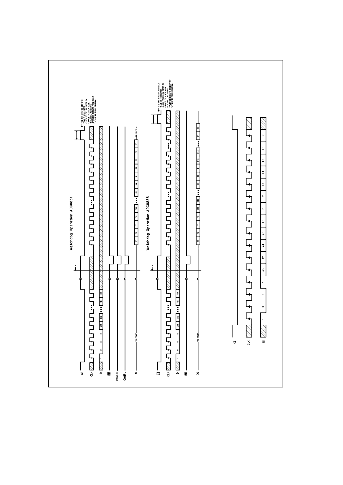
Watchdog Timing
TL/H/11021– 12
A/D Conversion Timing
TL/H/11021– 13
Timing Diagrams for ADC0851 and ADC0858
Read Power Flag after Power Up ADC0851/ADC0858
TL/H/11021– 14
8
Timing Diagrams for ADC0851 and ADC0858 (Continued)
TL/H/11021– 15
Write 1 Limit to ADC0851/ADC0858
TL/H/11021– 16
9
Timing Diagrams for ADC0851 and ADC0858 (Continued)
Write all Limits to ADC0851/ADC0858
TL/H/11021– 17
Read 1 Limit from ADC0851/ADC0858
TL/H/11021– 18
Read all Limits from ADC0851/ADC0858
TL/H/11021– 19
10
Timing Diagrams for ADC0851 and ADC0858 (Continued)
1 A/D Conversion ADC0851/ADC0858
TL/H/11021– 20
Auto A/D Conversion ADC0851/ADC0858
TL/H/11021– 21
11

ADC0851 Programming Chart
Function
Receive (DI) Transmit
Comments
Mode
(DO)
Watchdog 1000 C11...C0 T3...T0,C11...C0,P,S3...S0 Send Data after INT
Write 1 Limit 1001 A3...A0,L0...L7 Write Limit to RAM
1 A/D Conversion 1010 I3...I0 D0...D7,I3...I0 Send Data after Conversion
Read 1 Limit 1011 A3...A0 L0...L7 Send Limit from RAM
Test 1100 Do Not Use (See Text)
Write all Limits 1101 4 Bytes, L0 First Write All Limits to RAM
Auto A/D Convert 1110 C11...C0 D0...D7,I3...I0 Continuous Conversion
Read all Limits 1111 4 Bytes, L0 First Send all Limits from RAM
ADC0858 Programming Chart
Function
Receive (DI) Transmit
Comments
Mode
(DO)
Watchdog 1000 C11...C0 T3...T0,C11...C0,P,S15...S0 Send Data after INT
Write 1 Limit 1001 A3...A0,L0...L7 Write Limit to RAM
1 A/D Conversion 1010 I3...I0 D0...D7,I3...I0 Send Data after Conversion
Read 1 Limit 1011 A3...A0 L0...L7 Send Limit from RAM
Test 1100 Do Not Use (See Text)
Write all Limits 1101 16 Bytes, L0 First Write all Limits to RAM
Auto A/D Convert 1110 C11...C0 D0...D7,I3...I0 Continuous Conversion
Read all Limits 1111 16 Bytes, L0 First Send all Limits from RAM
Serial Communication Bit Order
Bit Order
Information Type ADC0851 ADC0858
First Last First Last
Limit Data L0 . . . L7 L0 . . . L7
A/D Conversion Data D0 . . . D7 D0 . . . D7
Limit Address A3 . . . A0 A3 . . . A0
Status S3 . . . S0 S15 . . . S0
Channel Tag T3 . . . T0 T3 . . . T0
Channel Configuration C11 . . . C0 C11 . . . C0
Channel Information I3 . . . I0 I3 . . . I0
Mode M3 . . . M0 M3 . . . M0
Power Fail P (One Bit) P (One Bit)
12

Pin Descriptions
V
CC
Positive power supply pin. Bypass to analog
ground with a 0.1 mF ceramic capacitor in
parallel with a 10 mF tantalum capacitor.
OSC Input/Output pin used to generate internal
timing for A/D conversion. This pin is connected to an external resistor and capacitor
to set the oscillation frequency for analog
timing (see
Figure 12
).
CS This is the chip select input pin. It must be
held low while data is transferred to or from
the ADC0851/8 (see Timing Diagram).
CLK The serial clock input pin is used to clock
serial data either into the data input pin (DI)
or out of the data output pin (DO). Input data
is loaded on the rising edge of CLK and the
output data is valid at the falling edge of
CLK.
DI Serial data digital input pin.
DO TRI-STATE data output pin.
INT
This is the active low interrupt pin that indicates that at least one analog input channel
voltage level has exceeded the programmed window limits. Since this pin has
an open drain output, an external pull up resistor is required. This allows many devices
to be wire-ORed together using a single
pull-up resistor.
EOC End of conversion output pin. The low state
indicates that an A/D conversion is in progress. The EOC pin goes high when the conversion is completed.
AGND Analog ground reference.
DGND Digital ground reference for the logic inputs.
Both AGND and DGND should be at same
potential.
V
REF
This is the analog reference pin. The voltage applied to this pin sets the full scale
A/D conversion range. Recommended voltages applied to this pin range from 1V to
V
CC
. Bypass to analog ground with a 0.1 mF
ceramic capacitor in parallel with a 10mF
tantalum capacitor.
COM The COM pin functions as an inverting dif-
ferential input common to all analog inputs
when each channel is configured as a single-ended channel. If the input channels are
programmed as differential pairs then the
COM input has no effect.
CH0–CH1 CH0– CH7 are analog input channels which
(ADC0851) can be configured as single ended inputs or
as differential pairs. The analog input volt-
CH0–CH7
age should stay within the power supply
(ADC0858)
range.
COMPL, These output pins are available only on the
COMPH ADC0851. During ‘‘Watchdog’’ operation, if
either of the inputs exceeds the window limits, not only is an interrupt generated but
also the COMPL and COMPH pins go low to
indicate whether the upper or lower boundary was exceeded (See applications section
for more information.)
13

General Overview
The ADC0851/58 is a versatile microprocessor-compatible
data acquisition system with an on-board watchdog capability. The device is capable of synchronous serial interface
with most microprocessors and includes a multiplexer, a
RAM and a successive approximation register. The
ADC0851 and the ADC0858 have two and eight input channels respectively.
1.0 Modes of Operation
The device can be used in any one of the eight modes of
operation listed below. A mode is selected by taking CS
low
and providing the IC with an input word whose first four bits
specify the desired mode (see the ‘‘Programming Charts’’
for the mode selection codes):
1.1 WATCHDOG MODE
This mode of operation allows the device to operate as a
digitally-programmable window comparator. The analog input voltage at each channel is compared against the upper
and lower boundary limits stored in an internal RAM. When
an input falls outside of its programmed window limits, an
interrupt is generated. The microprocessor can then pull CS
low which causes the device to produce a bit stream that
indicates which channel(s) crossed which limit(s).
The watchdog mode is selected by taking CS
low and shifting in the four bit word (1000) followed by a twelve bit
word that configures the analog inputs to operate either as
single-ended or as differential pairs (CH0 –CH1, CH2 –CH3,
etc.). When a channel is operating single-ended, its input
voltage is compared to the upper and lower limits stored in
RAM for that input. When two inputs are configured as a
differential pair, the limits stored in the RAM for the channel
with the lower number will be compared against the differential input voltage. For example, the differential voltage
CH0–CH1 will be compared with the lower and upper limits
for CH0. The limits are programmed using the ‘‘write one
limit to RAM’’ or ‘‘write all limits to RAM’’ mode.
Data Input (DI) WordÐADC0851 or ADC0858
TL/H/11021– 23
1.2 WRITE ONE LIMIT TO RAM
This mode allows the user to update a single limit for one of
the input channels. This is accomplished by using a 16-bit
stream of input data (see ‘‘Programming Chart’’). The first
four bits (1001)select the mode, the next four bits select
the input channel and the limit (upper or lower) that will be
preset, and the last eight bits set the limit (or comparator
threshold).
The limit data representing the input voltage limit (or comparator threshold) is expressed as per the following equation:
V
LIM
e
V
REF
((/2 L7a(/4 L6a...a1/256 L0)
where L7 is the MSB.
Data Input (DI) WordÐADC0851 or ADC0858
TL/H/11021– 24
1.3 WRITE ALL LIMITS TO RAM
This mode is used to update each pair of lower and upper
limits for all channels. This is accomplished by a stream of
input data whose first four bits select the mode of operation
followed by four bytes of limit data for the ADC0851 and
sixteen bytes of limit data for the ADC0858.
The limit data representing the input voltage limit (or comparator threshold) is expressed as per the following equation:
V
LIM
e
V
REF
((/2 L7a(/4 L6a...a1/256 L0)
where L7 is the MSB.
Data Input (DI) WordÐADC0851 or ADC0858
TL/H/11021– 25
1.4 READ ONE LIMIT FROM RAM
When the ADC0851/8 is configured in this mode, the user
can read back an 8-bit limit word from the RAM memory
location pointed to by the limit address. An 8-bit input word
selects the mode (1011) andthe memory location to be
read.
Data Input (DI)ÐADC0851 or ADC0858
TL/H/11021– 26
14

1.0 Modes of Operation (Continued)
1.5 READ ALL LIMITS FROM RAM
This mode of operation allows the device to serially output
8-bit limit data from each memory location in succession
starting with CH0-lower limit (see Section 2.4 under interface considerations).
Data Input (DI) WordÐADC0851 or ADC0858
TL/H/11021– 27
1.6 INITIATE ONE A/D CONVERSION
At any time, the user can initiate an A/D conversion on any
input channel. Note that the input channels may be configured as single ended or differential inputs. The first four bits
of the input word select the mode of operation and the next
four bits assign the multiplexer configuration.
Data Input (DI) WordÐADC0851 or ADC0858
TL/H/11021– 28
1.7 INITIATE AUTO A/D CONVERSION
When configured in this mode, an A/D conversion is done
on a channel or channel pair and after the output data is
transmitted, conversion begins on the next subsequent
channel or channel pair. In this mode the device continually
scans through the input channels making A/D conversions
unless the device’s mode of operation is changed. The first
four bits of the input word select the mode of operation and
the next twelve bits assign the multiplexer configuration.
Data Input (DI) WordÐADC0851 or ADC0858
TL/H/11021– 29
1.8 TEST MODE
This mode is used to test the ADC0851/8 at the factory and
is not intended for normal use. If this mode is accidentally
selected, the supply voltage must be disconnected and then
reconnected to reset the device.
2.0 Conversion Timing vs
Serial Interface Timing
Note that the ADC0851/8 uses two clock signals for proper
operation. Connecting an external resister (R
ext
) from the
OSC pin (pin 2) to V
CC
and an external capacitor (C
ext
) from
the OSC pin to ground causes the device’s internal oscillator to generate the OSC clock signal for A/D conversion
and watchdog timing. With R
ext
e
3.16 kX and C
ext
e
170 pF, the OSC clock frequency is approximately 1 MHz.
Note that internally, ADC0851/8 divides the OSC clock frequency by two. An A/D conversion is completed in eighteen
OSC clock periods maximum. It should be noted that the
OSC pin of the ADC0851/8 should not be driven by an external clock.
An external clock signal is applied to the CLK pin (pin 4) of
the ADC0851/8. The CLK signal is used to clock serial data
either into the data input pin (DI) or out of the data output
pin (DO).
Note that input data is loaded at the rising edge of CLK
while the output data is valid at the falling edge of CLK. All
digital timing such as data set-up and hold times and delays
are measured with respect to the CLK signal. The OSC
clock and CLK frequencies need not be the same.
3.0 Programming Information
The ADC0851 and ADC0858 communicate data serially
over the DI (data input) and DO (data output) lines. The data
format for the input and output words for various modes of
operation are shown in the ‘‘programming charts.’’
There are nine types of data as shown in the ‘‘serial communication bit order’’ table. The order in which data is communicated is MSB first in all but two cases: Limit data and
A/D conversion data. The various data types are described
below.
3.1 LIMIT DATA (L0, L1,...L7)
Limits on the ADC0851/8 are 8 bits in width and can either
represent an upper or lower boundary limit. Limit data can
either be written (in the ‘‘write one limit’’ or ‘‘write all limits’’
mode) to or read (in the ‘‘read one limit’’ or ‘‘read all limits’’
mode) from the limit RAM. Being able to read back the limit
data allows system testability, and it also allows independent software routines to see what window limits were previously written to the chip. During watchdog operation, a programmed limit must be crossed in order to cause an interrupt.
3.2 A/D CONVERSION DATA (D0, D1,...D7)
There are two A/D conversion modes (One A/D conversion
and Auto A/D conversion) that produce 8-bit conversion
data. During either type of A/D conversion, a single-ended
analog input or a differential analog input pair is digitized to
produce this conversion data.
3.3 LIMIT ADDRESS (A3, A2,...A0)
The limit address points to the location, within the limit
RAM, to which limit data is sent or from which it is received.
Limit address is used in the ‘‘write one limit to RAM’’, ‘‘write
all limits to RAM’’, ‘‘read one limit from RAM’’ or ‘‘read all
limits from RAM’’ mode. There are two addresses for each
analog input; the even addresses correspond to the lower
15

3.0 Programming Information
(Continued)
limits while the odd addresses correspond to the upper limits. The ADC0851 and ADC0858 both use four bits (A3–A0)
to address the limit RAM but the ADC0851 only decodes
the two LSBs while ignoring the two MSBs. The ADC0858
decodes all four bits thus yielding sixteen limit addresses.
3.4 STATUS AND CHANNEL TAG DATA
(S3, S2, . . . , S0, ADC0851; S15, S14, . . . , S0, ADC0858)
(T3, T2, . . . , T0)
During watchdog mode, immediately after one analog input
is determined to be outside of its programmed window limit,
its channel number is stored in the channel tag register and
the remaining inputs are checked one more time and the
pass/fail status of each input is stored in the status register.
When the microprocessor receives the interrupt signal, it
can read the status and channel tag data by pulling CS
low
and clocking out the data.
3.5 CHANNEL CONFIGURATION DATA
(C11, C10,...C0)
The channel configuration data assigns the configuration of
the multiplexer. The data is comprised of twelve bits with
each group of three bits addressing an analog input channel
pair. Each channel pair can be configured for single-ended
operation, differential operation, one single ended channel
and one disabled channel, or both channels disabled. The
channel configuration data is required when the device is in
the watchdog or Auto A/D conversion mode.
3.6 CHANNEL INFORMATION DATA
(I3, I2,...I0)
This data is used by the ADC0851/8 only when the device is
configured in the ‘‘One A/D conversion’’ mode. The channel information data assigns the configuration of the multiplexer.
3.7 MODE ADDRESS (M3, M2,...M0)
The input word (DI) configures the ADC0851/8 for various
modes of operation. The first four bits of the input word
constitute the mode address which specifies the mode of
operation.
3.8 POWER FAIL BIT (P)
The ADC0851/8 is automatically configured to the watchdog mode upon power-up and an interrupt is immediately
generated after CS
is pulled high. Pulling CS low produces a
17-bit data stream. The seventeenth bit of the output word
DO in the watchdog mode is the power fail bit, P. If the
output data is read after power-up then P will be at logical
‘‘1’’. Changing the mode of operation resets P to logical
‘‘0’’. Any subsequent power failure will cause the device to
configure in the watchdog mode upon power-up with P at
logical ‘‘1’’.
4.0 Initialization after Power-Up
The ADC0851/8 is automatically configured in the watchdog mode upon power-up. After reading the power fail bit
CS
is pulled high. To exit the watchdog mode and to change
to a new mode of operation, CS
should be high less than
eight oscillator clock periods for the ADC0851 and less than
thirty two oscillator clock periods for the ADC0858 respectively (see the Timing Diagram, ‘‘Read Power Flag after
Power Up ADC0851/8’’). When changing to a new mode of
operation, the device readies itself to read a new input word
clocked in at the data input (DI) pin. The input word configures the new mode of operation.
Functional Description
The simplified block diagram (
Figure 1
, front page) shows
the various functional blocks. The ADC0851 and ADC0858
include 2- and 8-channel analog input multiplexers respectively. Using the appropriate serial input word at the Data
Input (DI) pin, the analog channels can be configured for
either single-ended operation or differential mode operation.
The COM input pin provides additional flexibility since the
COM pin functions as an inverting differential input common
to all analog inputs when each channel is configured as a
single ended channel. Applying an external DC voltage at
the COM pin allows offsetting the single ended analog input
voltages from ground (pseudo-differential mode). Input
channels that are configured as differential pairs will be unaffected by the voltage at COM pin.
The ADC0851/8 includes an 8-bit DAC, a comparator and
an 8-bit successive approximation register. An analog-todigital conversion can be initiated at any time on any one of
the input channels. The 8-bit digital word corresponding to
the analog input voltage is serially clocked out at the Data
Output (DO) pin. In addition to its use as a multiplexed A/D
converter, the ADC0851/8 may also be used as a window
comparator in the watchdog mode. An upper and lower
boundary limit corresponding to each analog input voltage
may be stored in an internal RAM. The RAM consists of
sixteen memory locations, each 8 bit wide; however, for the
ADC0851 only four memory locations are used. Limit data
can either be written into or read back from the RAM. The
read/write capability allows independent software routines
to read back previously programmed window limits. Furthermore, currently programmed limits may also be read back to
ensure system testability. An address register holds the addresses of the RAM’s memory locations where data may
either be stored or retrieved from.
When the device is operated in the watchdog mode (as described in the ‘‘general overview’’ section), the analog inputs are continually polled and compared against their respective window limits. Once an input signal that has exceeded either boundary limit is detected, a ‘‘1’’ is stored in
the MSB position in a 16-bit status register, indicating a limit
crossing. Note that the ADC0851 uses only four locations of
the status register because it has only four limits. In addition, the tag register is updated so that the register holds the
address which indicates the channel and the corresponding
upper or lower limit that was crossed. After the first limit
crossing is detected, the device cycles through the remaining limits and compares them against their respective input
signals. If any additional limit crossing is or are detected
then a ‘‘1’’ is stored in the appropriate locations of the
status register. After the completion of this operation, the
interrupt pin (INT
) goes low, providing a flag to a microprocessor. The microprocessor can then cause the serial status
data to be shifted out by bringing the CS
line low. Together
with the status and tag bits, the microprocessor can determine which channel exceeded which limit. If desired the mi-
16

Functional Description (Continued)
croprocessor can then initiate an A/D conversion on any
channel(s). The ADC0851 includes two additional output
pins, COMPL and COMPH. During watchdog operation, if
either of the inputs exceeds its respective window bounds
then not only is an interrupt generated but a logic low at
COMPL or COMPH indicates whether the lower or upper
boundary was crossed.
A mode register within the ADC0851/8 allows the device to
be used in any one of the eight modes of operation as described in the ‘‘general overview’’ section.
The features described make the ADC0851/8 ideal for use
in microprocessor-based automotive, instrumentation and
control applications. Such applications often require monitoring of various transducer signals and comparison against
pre-programmed window limits. With its watchdog operation, the ADC0851/8 frees up the microprocessor from having to continually monitor the analog variables; the microprocessor is interrupted only when the input signal crosses
the preset bounds. Furthermore, the window limits can easily be changed with simple software control.
Applications Information
I. Digital Interface Considerations
The ADC0851 and ADC0858 communicate data serially
over the DI (Data Input) and DO (Data Output) pins. The
data transfer is synchronous with the external clock (CLK)
signal and is clocked in or out of the device at the rising
edge of clock. Note that although the output data is clocked
out starting at the rising edge of CLK, the data is valid at the
falling edge of CLK.
All internal timing in the device is with respect to the oscillator clock. The oscillator frequency is set by connecting a
resistor from the OSC pin (pin 2 for ADC0851 or ADC0858)
to V
CC
and a capacitor from the OSC pin to ground. The
period of the oscillator clock will determine the A/D conversion time and chip select (CS
) high duration as will be dis-
cussed in the following sections.
1.0 Modes of Operation
To initiate the operation of the device in any one of the eight
modes, the chip select (CS
) line must go low. After a CS low
is detected, serial input data at the DI pin is clocked in starting at the first rising edge of the serial clock. The first four
bits of the input word are reserved for specifying the mode
of operation, with the first bit of the input word always being
a logic ‘‘1’’. Table I shows the mode addresses for selecting
the different modes of operation.
TABLE I. Modes of Operation
Mode Address
Mode
M3 M2 M1 M0
1 0 0 0 Watchdog
1 0 0 1 Write One Limit
1 0 1 0 One A/D Conversion
1 0 1 1 Read One Limit
1 1 0 0 Test (for Factory Use Only)
1 1 0 1 Write All Limits
1 1 1 0 Auto A/D Conversion
1 1 1 1 Read All Limits
1.1 POWER FAILURE DETECTION/
INITIALIZATION AFTER POWER-UP
Upon power up, the device is automatically configured in the
watchdog mode. The status of the power flag bit, P, provides power failure indication to the microprocessor. The
timing diagram of
Figure 2
shows the sequence of events.
First consider the case of initial power up. After power is
applied, CS
should be brought high. Bringing CS high caus-
es the INT
pin to go low, which signals the microprocessor
that a failure has occurred. The microprocessor can then
interrogate the device as to the type of failure by bringing
CS
low. When CS goes low, it resets the INT pin to high and
the output data is read starting at the first rising edge of
clock (CLK) after CS
has gone low. Since this is the first
read cycle after power up, the power flag bit, P, is set high
and appears at the rising edge of the seventeenth clock
cycle after CS
low is detected
(Figure 2)
. After the power
flag is read by the microprocessor, CS
is taken high. Note
that the duration for which CS
remains high (after the power
flag is read) must be less than eight oscillator clock periods
for ADC0851 and less than thirty-two oscillator clock periods for ADC0858. This is required to interrupt the device
from watchdog mode so that when CS
goes low, the device
reads a valid data input (DI) word and configures to a new
mode.
During normal operation, the power flag bit is reset to zero
after the first ‘‘read’’ cycle and will be updated to a ‘‘1’’ only
if a power interruption occurs.
TL/H/11021– 30
FIGURE 2. Read Power Flag after
Power Up ADC0851/ADC0858
17

2.0 Memory Access Modes
The ADC0851/8 has an internal RAM with sixteen memory
locations (one location for the upper limit and one for the
lower limit for each of the 8 input channels). Each memory
location is 8 bits wide. An 8-bit limit word representing an
upper or lower limit boundary can either be written to or read
from the RAM. The ADC0851 uses only four memory locations for the four boundary limits corresponding to the two
inputs. The eight channel ADC0858, however, makes use of
all sixteen memory locations.
Each memory location is accessed by a specific address as
shown by Table II(a) and (b). Note that even addresses correspond to the lower limits while the odd addresses correspond to the upper limits. The ADC0851 and ADC0858 both
use 4 bits (A3, . . . A0) to address the RAM, however,
ADC0851 decodes only the two LSBs of the address data
while ignoring the two MSBs.
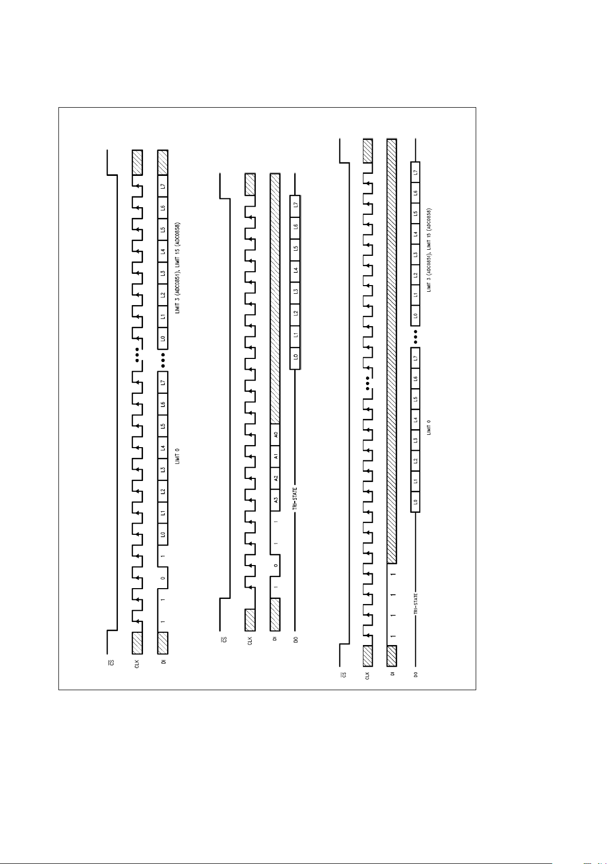
TABLE IIa. RAM Address and
Limit Data for ADC0851
RAM Address
Corresponding
Channel and Limit
A3 A2 A1 A0
X X 0 0 CH0 – Lower Limit
X X 0 1 CH0 – Upper Limit
X X 1 0 CH1 – Lower Limit
X X 1 1 CH1 – Upper Limit
Limit Data (ADC0851)
L0 L1 L2 L3 L4 L5 L6 L7
TABLE IIb. RAM Address and
Limit Data for ADC0858
RAM Address
Corresponding
Channel and Limit
A3 A2 A1 A0
0 0 0 0 CH0– Lower Limit
0 0 0 1 CH0– Upper Limit
0 0 1 0 CH1– Lower Limit
0 0 1 1 CH1– Upper Limit
0 1 0 0 CH2– Lower Limit
0 1 0 1 CH2– Upper Limit
0 1 1 0 CH3– Lower Limit
0 1 1 1 CH3– Upper Limit
1 0 0 0 CH4– Lower Limit
1 0 0 1 CH4– Upper Limit
1 0 1 0 CH5– Lower Limit
1 0 1 1 CH5– Upper Limit
1 1 0 0 CH6– Lower Limit
1 1 0 1 CH6– Upper Limit
1 1 1 0 CH7– Lower Limit
1 1 1 1 CH7– Upper Limit
Limit Data (ADC0858)
L0 L1 L2 L3 L4 L5 L6 L7
2.1 WRITE ONE LIMIT
This mode is used to update a single memory location in the
limit RAM. An 8-bit limit word is written to the location pointed to by the limit address. From Table I we can see that to
initiate the operation of the device in the ‘‘write one limit’’
mode, the mode address has to be1001.Thedata format
for the input word is as shown below.
Data Input (DI) WordÐADC0851 or ADC0858
TL/H/11021– 31
18

2.0 Memory Access Modes (Continued)
Note that the memory address is clocked in with the MSB
(bit A3) first whereas the limit data is clocked in with the LSB
(bit L0) first.
Figure 3
shows the timing diagram for writing one limit. After
CS
is brought low, the input word (DI) is clocked in starting
at the first rising edge of CLK. Taking CS
high after the MSB
(bit L7) of the limit data is loaded completes the write operation.
2.2 WRITE ALL LIMITS MODE
This mode is used to update all memory locations in the limit
RAM. An 8-bit limit word is written to each memory location.
Note that there are four limit words for the ADC0851 and
sixteen limit words for the ADC0858. To initiate the operation of the device in the ‘‘write all limits’’ mode, the mode
address has to be1101(see Table I). The data format for
the input word is as shown below.
Data Input (DI) WordÐADC0851 or ADC0858
TL/H/11021– 32
When writing all limits, memory address is not required. The
limit data is sequentially written into the RAM starting at the
location for CH0 – Lower Limit and ending at; CH1 –Upper
Limit for the ADC0851 (see Table IIa), CH7 –Upper Limit for
ADC0858 (see Table IIb). Note that L0 corresponds to the
LSB of the limit data.
Figure 4
shows the timing diagram. After CS is brought low,
the input word (DI) is clocked in starting at the first rising
edge of CLK. The first four bits of D1 configure the device in
the ‘‘write all limits’’ mode. Next, the limit data is serially
clocked in. To complete the operation, CS
should be
brought high after the data is loaded.
2.3 READ ONE LIMIT MODE
When the mode address is1011,thedevice is configured
in the ‘‘read one limit’’ mode. One 8-bit limit word can be
read from the RAM memory location pointed to by the limit
address. The data format for the input word is as shown
below.
Data Input (DI)ÐADC0851 or ADC0858
TL/H/11021– 33
TL/H/11021– 34
FIGURE 3. Timing Diagram for Write One Limit
TL/H/11021– 35
FIGURE 4. Timing Diagram for Write All Limits
19

2.0 Memory Access Modes (Continued)
The address bits access specific memory locations as per
Table II(a) and (b) for the ADC0851 and ADC0858 respectively. The address data is clocked in with the MSB (bit A3)
first.
The timing diagram in
Figure 5
shows that after CS goes
low, the first four bits of the input word configure the device
to ‘‘read one limit’’ mode. Next, the address bits select the
desired memory location. Third clock rising edge after the
address data’s LSB is loaded, the limit data is output with
the LSB (bit L0) first.
2.4 READ ALL LIMITS MODE
With a mode address of1111,thedevice is configured in
the ‘‘read all limits mode’’. When in this mode, 8-bit limit
data from each memory location is serially transmitted out.
The data format for the input word is as follows:
Data Input (DI) WordÐADC0851 or ADC0858
TL/H/11021– 36
Note that no memory address data is required. The limit
data is sequentially transmitted out starting from the memory location for CH0 –Lower Limit and ending at; CH1 – Upper
Limit for the ADC0851 (see Table II(a)), CH7 –Upper Limit
for the ADC0858 (see Table II(b)).
The timing diagram of
Figure 6
shows that the input data is
loaded starting at the first rising edge of CLK after CS
goes
low. Third clock rising edge after the last bit of the input data
is loaded, the limit data is serially transmitted out. Four limit
words are transmitted for the ADC0851; sixteen for the
ADC0858. Each limit word is output with the LSB (bit L0)
first. Taking CS
high after the MSB of the last limit data is
transmitted completes the operation.
TL/H/11021– 38
FIGURE 5. Timing Diagram for Read One Limit ADC0851/ADC0858
TL/H/11021– 39
FIGURE 6. Timing Diagram for Read All Limits ADC0851/ADC0858
20

3.0 Watchdog Mode
This is the primary real time operating mode. During watchdog operation, the upper and lower limits stored in the RAM
are applied sequentially to the DAC’s digital inputs. The
DAC’s analog output is applied to the comparator input and
compared against the voltage at the enabled analog input
pin. The data format for the input word is as shown below.
Data Input (DI) WordÐADC0851 or ADC0858
TL/H/11021– 37
The last twelve bits of the input word assign the multiplexer
channel configuration.
3.1 SELECTING THE CHANNEL CONFIGURATION
When the device is either in the watchdog or automatic A/D
conversion mode, each pair of analog input channels must
be programmed to determine which channel(s) will be active, and whether they will be operating single-ended or differentially. Table III(a) and (b) show the channel addresses
for the ADC0851 and the ADC0858 in various channel configurations. When the channels are configured as singleended inputs, the input voltages are measured with respect
to the voltage at the COM pin. Applying a DC voltage at the
COM pin will cause the device to measure the difference
between the input signal and the voltage at the COM pin.
The voltage at the COM pin has no effect on an input channel that is configured as a differential pair. When the channel pairs are configured as differential inputs (i.e., CH0 –
CH1, CH2 –CH3, etc.) the differential voltage is compared
with the limits for the lower numbered channel. For example, the differential voltage CH0– CH1 will be compared with
the limits for CH0. Note that the channel pairs are programmed in groups of three bits. The channel address is
input to the A/D converter with the MSB (bit C11) first.
The timing diagrams for ADC0851 and ADC0858 watchdog
operation are shown in
Figure 7
. After a CS low is detected,
the input word (DI) is clocked in starting at the first rising
edge of the serial clock (CLK). Once the least significant bit
of the channel address is loaded, CS
should go high. Taking
CS
high after the proper input word is loaded initiates the
operation of the device in the watchdog mode. To keep the
device in continuous watchdog mode, CS
should remain
high for eight or more OSC clock periods for the ADC0851
and thirty-three or more OSC clock periods for the
ADC0858. If the input signals are within the boundary limits,
the interrupt pin (INT) remains at logic ‘‘1’’ and the Data
Ouptut (DO) pin is in TRI-STATE. In addition, in the case of
the ADC0851, the COMPL and COMPH pins remain at logic
‘‘1’’.
TABLE IIIa. Multiplexer Channel Configuration (ADC0851)
TL/H/11021– 40
TABLE IIIb. Multiplexer Channel Configuration (ADC0858)
TL/H/11021– 41
21

3.0 Watchdog Mode (Continued)
TL/H/11021– 42
FIGURE 7. Timing Diagrams for Watchdog Operation
22

3.0 Watchdog Mode (Continued)
The device will read the new input word and configure to a
different mode if CS
is high for less than eight oscillator
clock periods for the ADC0851 and less than thirty-two oscillator clock periods for the ADC0858.
Once a boundary limit is crossed, INT
goes low. Moreover,
for ADC0851, COMPL goes low if a lower limit is crossed,
whereas COMPH goes low if an upper limit is crossed. If the
input signals exceed both the upper and lower boundary
limits then both COMPL and COMPH would go low.
To output data after a limit crossing occurs (i.e., after INT
goes low), CS should be brought low. Note that INT,
COMPL and COMPH would remain low as long as CS
doesn’t go low. After CS
goes low INT, COMPL and
COMPH go high and one clock cycle later output data is
transmitted starting at the first rising edge of CLK, however,
the data is valid at the falling edge of CLK (
Figure 7
).
3.2 LIMIT CROSSING DETECTION
When the ADC0851/8 is configured in the watchdog mode,
the device operates as a window comparator. First the lower window limit (stored in the RAM) for CH0 is compared
against the input voltage at CH0. If the input voltage is
greater than the lower limit, then no interrupt is generated.
Next the upper window limit for CH0 is compared against
CH0 input voltage. If the input voltage is less than the upper
window limit then no interrupt is generated for CH0 and the
device starts a similar comparison cycle for the next channel (CH1). Note that the lower limit can be greater than the
upper limit; in this case the device will flag the microprocessor if the input signal falls inside a window.
TABLE IVa. Channel Tag Address
and Status (ADC0851)
Tag Tag Address Corresponding Limit
Ý
T3 T2 T1 T0
and Channel
0 0000Lower LimitÐCH0
1 0001Upper LimitÐCH0
2 0010Lower LimitÐCH1
3 0011Upper LimitÐCH1
TL/H/11021– 43
TABLE IVb. Channel Tag Address
and Status (ADC0858)
Tag Tag Address Corresponding Limit
Ý
T3 T2 T1 T0
and Channel
0 0000Lower LimitÐCH0
1 0001Upper LimitÐCH0
2 0010Lower LimitÐCH1
3 0011Upper LimitÐCH1
4 0100Lower LimitÐCH2
5 0101Upper LimitÐCH2
6 0110Lower LimitÐCH3
7 0111Upper LimitÐCH3
8 1000Lower LimitÐCH4
9 1001Upper LimitÐCH4
101010Lower LimitÐCH5
111011Upper LimitÐCH5
121100Lower LimitÐCH6
131101Upper LimitÐCH6
141110Lower LimitÐCH7
151111Upper LimitÐCH7
TL/H/11021– 44
Each comparison takes 2 ms; thus a total of 4 ms is required
per channel.
When in watchdog mode, the device will continuously cycle
through the input channels until an input that has crossed its
preset window limit is detected. When this occurs, a logical
‘‘1’’ is stored in the MSB (bit S3 for ADC0851 and S15 for
ADC0858) position of the status register. In addition the tag
register is updated with the channel’s address (see Tables
IV(a) and (b) for ADC0851 and ADC0858 respectively). Note
that the tag address indicates which channel crossed which
limit. Once the tag register is updated after the first limit is
crossed, the device will once more cycle through the remaining channels and compare the input voltages against
23

3.0 Watchdog Mode (Continued)
their respective window limits. A logical ‘‘1’’ will be placed in
the appropriate location of the status register for each limit
that is crossed as the device cycles through the remaining
channels. Note that the tag register is updated only once
i.e., when the first limit is exceeded. After the last limit comparison is made subsequent to the first limit crossing, the
device will cease any further limit comparisons and will
cause the interrupt pin to go low. Taking CS
low causes the
data in the status and tag registers to be transmitted along
with the programmed channel configuration information. In
addition, an extra bit, P, is inserted between the channel
and status information. This bit is updated to a logic ‘‘1’’ in
case of a power interruption.
The format for the output data is as shown below.
Data Output (DO) WordÐADC0851
TL/H/11021– 46
Data Output (DO) WordÐADC0858
TL/H/11021– 47
The order in which data is transmitted is as follows
(ADC0851 or ADC0858):
#
Tags (4 bits)ÐMSB (T3) first
#
Channel configuration (12 bits)ÐMSB (C11) first
#
Power interrupt (1 bit)
#
Status (4 bits for ADC0851, 16 bits for ADC0858)ÐMSB
(S3/S15) first
It is important to note that any channel that is disabled will
not cause an interrupt. Furthermore, when operated in the
differential mode, the arithmetic difference of the two voltages will be compared with the lower and upper limits for
the lower numbered channel. For example, with CH0 and
CH1 operating as a differential input pair, the CH0 limits will
apply.
Consider an example where the lower limit of CH1 is
crossed first and while the remaining limits are being
checked, the upper limit of CH0 is crossed.
Figure 8
illustrates the sequence of events for the ADC0851. During
watchdog operation, CH0’s lower limit stored in the RAM is
compared against the input voltage at CH0. Since no limit
crossing is detected, the upper limit is compared against
CH0 input voltage. Again no limit crossing is detected and
so CH1’s lower limit is next compared against the CH1 input
voltage. This time a limit crossing is detected and a logic
‘‘1’’ is now stored in the MSB (S3) position of the status
register (see Table IV(a)). Also the Tag register is updated
with the corresponding address (0010)from Table IV(a).
The device now cycles through the remaining channels
once more. Since no limit crossing is detected for the upper
limit of CH1, a logic ‘‘0’’ is stored for S2 of the status register. Similarly a logic ‘‘0’’ is stored for S1 of the status register. Finally to complete the cycle, the last limit (upper limit of
CH0) is checked and a limit crossing is detected. Consequently, a logic ‘‘1’’ is stored for S0. Note that the Tag regis-
ter is only updated once when the first limit crossing is detected thus indicating which channel first exceeded its lower
or upper limit.
TL/H/11021– 45
(Example: Lower limit of CH1 is crossed first. During cycle through, upper
limit of CH0 is crossed)
FIGURE 8. Example of Limit Crossing
Detection (ADC0851)
Assuming that there is no power interruption and that the
ADC0851 was configured for single ended operation, the
output word for our example would be:
(Example of ADC0851 Data Output. Single ended input.
Lower limit of CH1 fails first. During cycle through, upper
limitÐCH0 failure is detected).
0010 X X XXX...0 001001
T3 T2 T1 T0 C11 C10 C9 C8 C7 C1 C0 P S3 S2 S1 S0
XeDon’t care, whatever bit was initially programmed (ADC0851 only).
The ADC0858 operates similar to the ADC0851 except that
the ADC0858 has a 16-bit status word for the sixteen limits
and sixteen tag addresses (See Table IV(b)). The output
word transmitted to the microprocessor not only contains
information as to how the channels are configured but also
which input crossed which limit. If desired, the microprocessor can go through a status bit normalization routine to normalize the status information with the tag number as will be
discussed next.
3.3 STATUS BIT NORMALIZATION
Figure 9
shows the procedure for normalizing the status information. Let’s consider the example cited earlier for the
ADC0851. In our example, the lower limit of CH1 was
crossed first and during cycle-through, upper limitÐCH0
crossing was detected. The serial status data is thus1001
andthetagdata0010corresponds to tag
Ý
2 (see Table
IVa). Since the most significant bit (S3) of the status data is
transmitted first, the data stored in the microprocessor’s
memory is1001.Themicroprocessor next computes the
tag number from the tag data and rotates the status bits left
‘‘TAG’’ places as in
Figure 9
. For our example, the status
bits are rotated by shifting left 2 places. The status information in the microprocessor’s memory is now normalized i.e.,
U0 corresponds to tag 0, U1 corresponds to tag 1 and so
on. From the example in
Figure 9
we can see that the status
register in the microprocessor’s memory shows that tag 2
and tag 1 failed. The ADC0858 uses a 16-bit status word
and operates similar to the ADC0851. An example shown in
Figure 9
for the ADC0858 demonstrates how status bit nor-
malization is carried out.
24

3.0 Watchdog Mode (Continued)
TL/H/11021– 48
FIGURE 9. Status Bit Normalization
4.0 A/D Conversion Modes
The ADC0851/8 can be used in two A/D conversion
modes. In ‘‘One A/D conversion’’ mode, the device operates as a multiplexed A/D converter and a conversion may
be initiated on any channel or channel pair configured in the
differential mode. In the ‘‘Automatic A/D conversion’’ mode,
an A/D conversion is done on a channel or channel pair and
after the output data is transmitted, conversion begins on
the next subsequent channel or channel pair. This process
will continue unless the device’s mode of operation is
changed.
Note that the A/D conversion time is determined by the
oscillator clock period and has no relation with the digital
clock signal, CLK. The oscillator clock’s frequency is set by
connecting a resistor from the OSC pin (pin 2 for ADC0851
or ADC0858) to V
CC
and a capacitor from the OSC pin to
ground. The conversion time of the A/D converter is eighteen OSC clock periods maximum. Assuming that the oscillation clock frequency is set at 1 MHz (with R
ext
e
3.16 kX
and C
ext
e
170 pF) then the conversion time would be
18 ms maximum.
4.1 ONE A/D CONVERSION MODE
This mode is used to initiate one A/D conversion on a single
channel or channel pair configured in the differential mode.
The necessary mode address as per Table I is1010.The
format for the input word is as follows:
Data Input (DI) wordÐADC0851 or ADC0858.
TL/H/11021– 49
(Table V(a) for ADC0851, Table V(b) for ADC0858)
The 4-bit data following the mode address is the channel
information address. These four bits assign the MUX configuration for the single A/D conversion. The channel information addresses and the corresonding MUX configurations
are shown in Table V(a) and (b) for ADC0851 and ADC0858
respectively. Note that the ADC0851 only decodes the two
LSBs of the channel information data while ignoring the two
MSBs (I3 and I2). When a channel pair is configured in the
differential mode, it is important to note that the arithmetic
difference of the channel voltages should not be negative.
Negative difference voltage would result in all zeroes at the
output.
TABLE V(a). Channel Information for
One A/D Conversion (ADC0851)
Channel Information
Channels Enabled
I3 I2 I1 I0
X X 0 0 CH0
X X 0 1 CH0– CH1
X X 1 0 CH1
X X 1 1 Invalid
25

4.0 A/D Conversion Modes (Continued)
TABLE V(b). Channel Information
for One A/D Conversion (ADC0858)
Channel Information
Channels Enabled
I3 I2 I1 I0
0000CH0
0 0 0 1 CH0– CH1
0010CH1
0 0 1 1 Invalid
0100CH2
0 1 0 1 CH2– CH3
0110CH3
0 1 1 1 Invalid
1000CH4
1 0 0 1 CH4– CH5
1010CH5
1 0 1 1 Invalid
1100CH6
1 1 0 1 CH6– CH7
1110CH7
1 1 1 1 Invalid
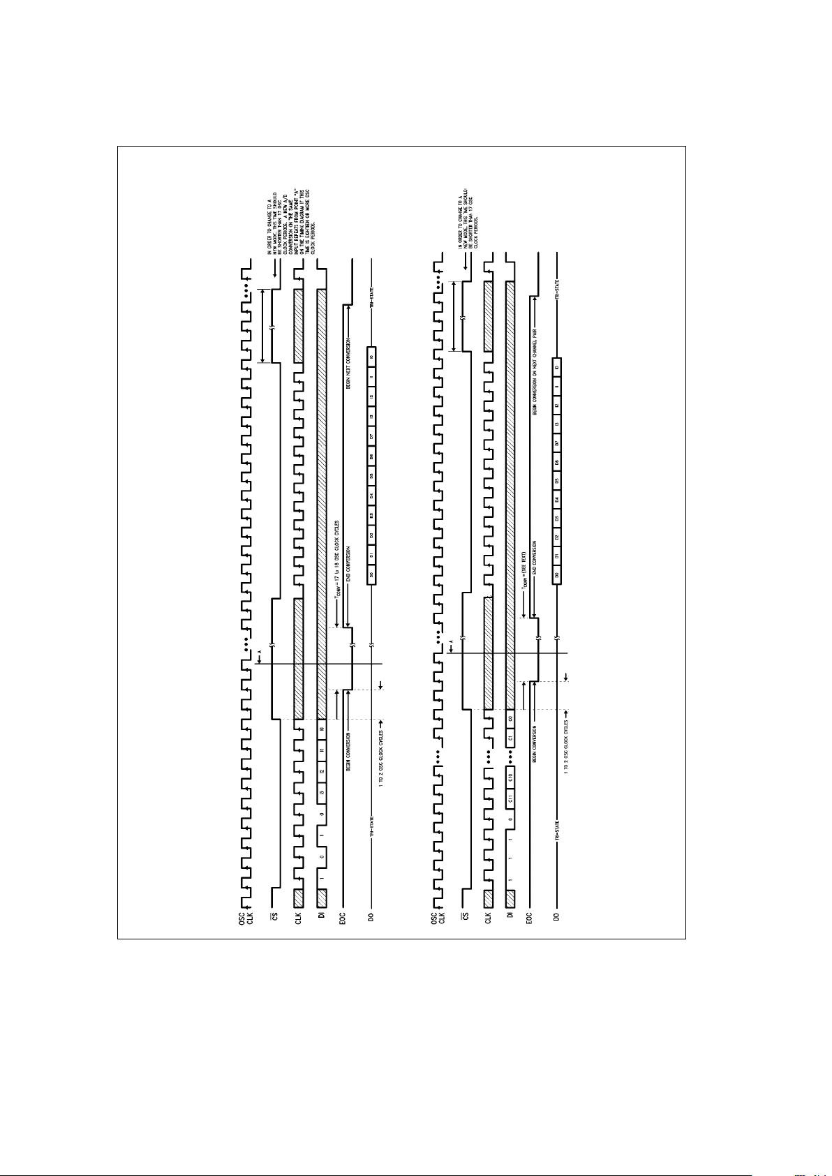
The timing diagram for one A/D conversion is shown in
Fig-
ure 10
. After CS goes low, the input word (DI) is clocked in
starting at the first rising edge of the digital clock signal,
CLK. The first four bits of the input word configure the device for ‘‘one A/D conversion’’ mode while the following
four bits (channel information address) assign the configuration of the MUX as per Table V(a) and (b) for the ADC0851
and the ADC0858 respectively. Any input data following the
channel information address is ignored until the device’s
mode of operation is changed.
Taking CS
high after the last bit of the channel information
address loads the input word. Had CS
been kept low longer,
the following bits of the input word would have been ignored. The device takes one to two OSC clock periods after
CS
goes high to initiate the start of A/D conversion. The
EOC output goes low, thus signalling the start of the conversion process. After a maximum of eighteen OSC clock periods, conversion is completed and EOC output goes high,
thus signalling the end of conversion. The output data is
now available and will be transmitted only if CS
is brought
low. The output data is transmitted starting at the first rising
edge of CLK after CS
goes low.
The format for the output word is as shown below.
Data Output (DO)ÐADC0851 or ADC0858
TL/H/11021– 50
The first eight bits of the output word represent the digital
equivalent of the input voltage. Bits I3 through I0 provide the
channel configuration information as per Table V(a) and (b)
for ADC0851 and ADC0858 respectively. Note that this information is the same as the channel information in the input word. The order in which the output data is transmitted
is as follows:
#
DataÐLSB (D0) first
#
Channel informationÐMSB (I3) first
Note that the output will be TRI-STATE if CS remains low
after I0 is transmitted. Taking CS
high after the output data
is transmitted causes the device to initiate the start of the
next A/D conversion on the same input while ignoring the
data input word (DI). If the duration for which CS
is high is
less than seventeen OSC clock periods, the conversion process will be interrupted and the device will look for the mode
address at the falling edge of CS
so as to configure to a new
mode of operation. However, if CS
is high for eighteen or
more OSC clock periods then the conversion operation will
continue from point A on the timing diagram
(Figure 10)
.
To ensure repetitive A/D conversion on the same input, CS
going low should be synchronized with EOC going high.
Thus after EOC goes high, the conversion is completed and
CS
can go low to transmit the output data. Meanwhile, if CS
goes low while EOC is low then the conversion process is
interrupted and the device is readied for a new mode of
operation.
4.2 AUTO A/D CONVERSION MODE
When used in this mode, the ADC0851/8 offers added flexibility that many multiplexed A/D converters don’t. In the
auto A/D conversion mode, the ADC0851/8 scans through
the selected input channels, performing A/D conversion on
each channel without the need for reloading a new data
input word each time. From Table I, the mode address for
the ‘‘Auto A/D Conversion’’ mode is1110.
The format for the input word is as follows:
Data Input (DI) WordÐADC0851 or ADC0858
TL/H/11021– 51
26

4.0 A/D Conversion Modes (Continued)
The 12-bit channel address following the mode address assigns the MUX configuration as per Table III(a) and (b) for
ADC0851 and ADC0858 respectively. Note that the
ADC0851 only decodes the three LSBs (C0, C1 and C2) of
the channel address.
The timing diagram for ‘‘Auto A/D Conversion’’ mode is
shown in
Figure 11
. The input word is loaded starting at the
first rising edge of the CLK after CS
goes low. The first four
bits configure the device for the ‘‘Auto A/D Conversion’’
mode while the 12-bit channel address assigns the configuration of each channel pair. If CS
remains low after C0 is
loaded then any subsequent input data is ignored. Taking
CS
high after the input word is loaded initiates the start of
A/D conversion. A/D conversion starts one to two OSC
clock periods after CS
goes high. The EOC output goes low
to signal the start of an A/D conversion. The conversion
time may range from 17 msto74ms depending on how
the channel pairs are configured. The EOC output goes high
at the end of conversion thus signalling that the result of the
A/D conversion can now be retrieved. The output data will
be transmitted only if CS
goes low and is transmitted start-
ing at the first rising edge of CLK signal after CS
goes low.
The format for the output word is as follows:
Data Output (DO)ÐADC0851 or ADC0858
TL/H/11021– 52
27

4.0 A/D Conversion Modes (Continued)
TL/H/11021– 53
FIGURE 10. Timing Diagram for One A/D Conversion ADC0851/ADC0858
TL/H/11021– 54
FIGURE 11. Timing Diagram for Auto A/D Conversion ADC0851/ADC0858
28

4.0 A/D Conversion Modes (Continued)
The first eight bits of the output word represents the digital
equivalent of the analog input voltage. Status bits I3 through
I0 provide the channel configuration information as per Table V(a) and (b) for ADC0851 and ADC0858 respectively.
Keeping CS
low after I0 is transmitted causes the output to
be TRI-STATE. Once the output data is transmitted, CS
may
go high to initiate the start of the next A/D conversion. The
subsequent A/D conversion starts on the next channel pair
that is configured as per the initially loaded input word
(Fig-
ure 11)
. Any data on the data input (DI) line is ignored. Note
that if the duration for which CS
is high is less than seventeen OSC clock periods then the conversion process would
be interrupted and the device would look for the mode address at the falling edge of CS
so that a new mode of opera-
tion can be configured.
To ensure proper operation in the ‘‘Auto A/D Conversion’’
mode, CS
going low should be synchronized with EOC going high. Thus after EOC goes high, the conversion is completed and CS
can go low to transmit the output data. After
the output data is transmitted, CS
should go high to initiate
automatic A/D conversion on the next channel pair and remain high until the conversion is completed and EOC goes
high. Meanwhile, if CS
goes low while EOC is low then the
conversion process is interrupted and the device is readied
for a new mode of operation.
5.0 Test Mode
A mode address of1100configures the device in the test
mode. This mode is used to test the internal operation of the
device at the factory and is not recommended for normal
use. If the device is accidentally configured in the test mode
then the power supply must be disconnected and reconnected again to reset the device.
6.0 Bidirectional I/O
If the microprocessor has bidirectional Input/Output capability then ADC0851/8’s input and output pins can be tied
together and a single wire can be used to serially input data
to or output data from ADC0851/8. This capability is made
possible because when the input word is clocked in, the
output pin is in TRI-STATE and when the output word is
clocked out, the data at the input pin is ignored.
II. Analog Considerations
1.0 A/D Conversion Time
The A/D conversion time is a function of the OSC clock
frequency. The oscillator frequency is set by connecting an
external resistor, R
ext
from the ADC0851/8’s OSC pin to
V
CC
and an external capacitor, C
ext
from the OSC pin to
ground. With R
ext
e
3.16 kX and C
ext
e
170 pF, the OSC
frequency is 1 MHz at V
CC
e
4.5V and 1.05 MHz at V
CC
e
5.5V.
The OSC frequency will vary as the ambient temperature
varies, this is shown by the Typical Performance Characteristics curve, ‘‘OSC Frequency vs Temperature’’. For a specified external resistor, the OSC frequency can be changed
by varying the external capacitor as is shown by the Typical
Performance Characteristics curve, ‘‘OSC Frequency vs
R
ext
and C
ext
’’. Note that the OSC pin of the ADC0851/8
should not be driven by an external clock as this might
cause improper operation. The A/D converter’s conversion
time is a minimum of seventeen OSC clock periods and a
maximum of eighteen.
Figure 12
shows a typical connection
for the ADC0851 and ADC0858.
2.0 The Reference
The magnitude of the reference voltage (V
REF
) applied to
the A/D converter determines the analog input voltage span
(i.e., the difference between V
IN(max)
and V
IN(Min)
) over
which the 256 possible output codes apply. The reference
voltage source connected to the V
REF
pin of ADC0851/8
must be capable of driving a minimum load of 4 kX.
The ADC0851/8 can be used in either ratiometric applications or in systems requiring absolute accuracy. In a ratiometric system, the analog input voltage is proportional to
the voltage used for the A/D’s reference. This voltage is
usually the system power supply, so the V
REF
pin can be
tied to V
CC
.
For absolute accuracy, where the analog input varies between very specific voltage limits, the reference pin must be
connected to a voltage source that is stable over time and
temperature. The LM385 and LM336 micropower references are good low current devices for use with these A/D
converters.
The maximum value of the reference voltage is limited by
the A/D converter’s power supply voltage, V
CC
. The minimum value, however, can be as low as 1V while maintaining
a typical Integral Linearity of
g
1 LSB (see Typical Performance Characteristics curve, ‘‘Linearity Error vs Reference
voltage’’). This allows direct conversion of transducer outputs that provide less than a 5V output span. Due to the
increased sensitivity of the A/D converter at low reference
voltages (e.g., 1 LSB
e
3.9 mV for a 1V full scale range),
care must be exercised with regard to noise pickup, circuit
layout, and system error voltage sources.
3.0 The Analog Inputs
3.1 REDUCING COMMON MODE ERROR
Rejection of common mode noise can be achieved by configuring the ADC0851/8’s inputs in the differential mode
since the offending common mode signal is common to
both the selected ‘‘
a
’’ and ‘‘b’’ inputs. The time interval
between sampling the ‘‘
a
’’ input and the ‘‘b’’ input is one
oscillator clock period. A change in the common-mode voltage during this short time interval can cause conversion errors. For a sinusoidal common-mode signal this error is:
V
error(Max)
e
V
PEAK
(2qfCM) (1/f
OSC
)
where fCMis the frequency of the common-mode signal,
V
PEAK
is the signal’s peak voltage and f
OSC
is the A/D
converter’s OSC clock frequency.
For a 60 Hz common-mode signal to generate a (/4 LSB
error (&5 mV for a 5V full scale range) with the converter
running at f
OSC
e
250 kHz, its peak voltage would have to
be 3.3V.
3.2 SOURCE RESISTANCE
For a source resistance under 2 kX, the ADC0851/8’s total
unadjusted error is typically
g
0.2 LSB at V
REF
e
4.75V and
f
OSC
s
1 MHz (see Typical Performance Characteristics
curves, ‘‘Total Unadjusted Error vs Source Impedance’’).
One source of error is the multiplexer’s leakage current of
3 mA which contributesa3mVdrop acrossa1kXsource
29

3.0 The Analog Inputs (Continued)
resistance. Another source of error is the sampling nature of
the A/D converter. Short spikes of current enter the ‘‘
a
’’
input and exit the ‘‘
b
’’ input at the rising and falling transition of the OSC clock . These currents decay rapidly and
generally do not cause errors since the internal comparator
is strobed at the end of a clock period. If large source resistances are used however, then the transients caused by the
current spikes may not settle completely before conversion
begins. If a capacitor is used at the input of the A/D converter for input filtering then the input signal source resistance
should be kept at 1 kX or less.
3.3 ANALOG INPUT PROTECTION
Often the analog inputs of A/D converters are driven from
voltage sources that can swing higher than V
CC
or lower
than GND. Analog inputs often come from op amps which
use
g
15V supplies. While during normal operation the input
voltages stay within the 0V –5V A/D converter supply voltage range, at power up the input voltage may actually rise
above or fall below the A/D converter’s supply voltages. If
the input voltage to any A/D converter input pin does fall
outside the supply voltage by more than 0.3V (worst case)
and the input draws more than 5 mA then there is a good
possibility that the converter may latch up and provide a low
impedance short between V
CC
and GND.
Figure 13
shows the overvoltage protection circuit for the
analog input. If, for instance, the amplifier’s output saturates
to its positive supply rail, then the junction of R1 and R2
would be clamped to V
CC
plus a diode drop. Resistor R1
limits the op amp’s output current and R2 limits the current
flowing into the input of the A/D converter. Likewise, the
junction of R1 and R2 would be clamped to a diode drop
below ground if the op amp’s output saturates to the negative rail.
4.0 Zero Scale and Full Scale
Adjustment
4.1 ZERO SCALE ERROR
The zero scale error of the A/D converter does not require
adjustment. If the minimum analog input voltage value,
V
IN(Min)
, is not at ground potential then a zero offset can be
done. The converter can be made to output 0000 0000 digital code for this minimum input voltage by biasing the V
IN(b)
input of a differential input pair at this V
IN(Min)
value. This
utilizes the differential mode operation of the A/D converter.
The zero scale error of the A/D converter relates to the
location of the first riser of the transfer function and can be
measured by grounding the V
IN(b)
input and applying a
small magnitude positive voltage to the V
IN(a)
input. Zero
error is the difference between the actual DC input voltage
(the ideal (/2 LSB value, (/2 LSB
e
9.8 mV for V
REF
e
5.000
V
DC
) and the applied input voltage that causes an output
digital code transition from 0000 0000 to 0000 0001.
4.2 FULL SCALE ADJUSTMENT
The full-scale adjustment can be made by applying an input
voltage that is 1.5 LSB less than the desired analog fullscale voltage and then adjusting the magnitude of the V
REF
input voltage for a digital output code that just changes from
1111 1110 to 1111 1111.
4.3 ADJUSTING FOR AN ARBITRARY
ANALOG INPUT VOLTAGE RANGE
Analog input voltages that span from a positive non-zero
minimum value can easily be accommodated by the
ADC0851/8. In this case, the A/D converter is used in the
differential mode and a reference voltage equal to V
IN(Min)
is applied to the V
IN(b)
input. Normally zero scale adjustment is not required because the zero scale error is very
small. However, if zero scale adjustment is desired then a
voltage equal to V
IN(Min)
plus (/2 LSB (where 1 LSBeInput
voltage span/256) should be applied to V
IN(a)
and the ref-
erence voltage at V
IN(b)
should be adjusted such that the
output code just changes from 0000 0000 to 0000 0001.
Once the proper reference voltage is applied to the V
IN(b)
input then full scale adjustment can be made. Full scale
adjustment is made by first applying a voltage to the V
IN(a)
input that is 1.5 LSB less than V
IN(Max)
i.e.;
V
IN(a)FSADJ
e
V
Max
b
1.5[(V
Max
b
V
Min
)/256
]
where, V
Max
e
the high end of the analog input voltage
range
V
Min
e
the low end of the analog input voltage
range
The reference voltage, V
REF
applied to the reference input
pin of the A/D converter is adjusted so that the output code
just changes from 1111 1110 to 1111 1111. This completes
the adjustment procedure.
Typical Applications
TL/H/11021– 55
FIGURE 12. Recommended Connection for ADC0851 and ADC0858
30

Typical Applications (Continued)
TL/H/11021– 56
FIGURE 13. Over Voltage Protection of the Analog Inputs
ADC0851
Single Ended
TL/H/11021– 57
Pseudo-Differential
TL/H/11021– 58
Differential
TL/H/11021– 59
FIGURE 14. Analog Input Multiplexer Options for ADC0851
ADC0858
Single Ended
TL/H/11021– 60
Pseudo-Differential
TL/H/11021– 61
Differential
TL/H/11021– 62
Mixed Mode
TL/H/11021– 63
FIGURE 15. Analog Input Multiplexer Options for ADC0858
31

Typical Applications (Continued)
TL/H/11021– 64
FIGURE 16. Adaptive Instrumentation Control
(Ratiometric Operation) with Over Range Flag
TL/H/11021– 65
FIGURE 17. Remote Temperature Sensor
with Over Range Flag
TL/H/11021– 66
FIGURE 18. Absolute Input with 2.5V Input Voltage Span
TL/H/11021– 67
FIGURE 19. Single Channel Ratiometric Operation
32

33

Physical Dimensions inches (millimeters)
16-Pin Ceramic DIP
Order Number ADC0851CMJ/883
NS Package Number J16A
20-Pin Ceramic DIP
Order Number ADC0858CMJ/883
NS Package Number J20A
34

Physical Dimensions inches (millimeters) (Continued)
16-Pin Plastic DIP
Order Number ADC0851BIN or ADC0851CIN
NS Package Number N16E
20-Pin Plastic DIP
Order Number ADC0858BIN or ADC0858CIN
NS Package Number N20A
35

ADC0851 and ADC0858 8-Bit Analog Data Acquisition and Monitoring Systems
Physical Dimensions inches (millimeters) (Continued)
20-Lead PLCC
Order Number ADC0851BIV, ADC0851CIV,
ADC0858BIV or ADC0858CIV
NS Package Number V20A
LIFE SUPPORT POLICY
NATIONAL’S PRODUCTS ARE NOT AUTHORIZED FOR USE AS CRITICAL COMPONENTS IN LIFE SUPPORT
DEVICES OR SYSTEMS WITHOUT THE EXPRESS WRITTEN APPROVAL OF THE PRESIDENT OF NATIONAL
SEMICONDUCTOR CORPORATION. As used herein:
1. Life support devices or systems are devices or 2. A critical component is any component of a life
systems which, (a) are intended for surgical implant support device or system whose failure to perform can
into the body, or (b) support or sustain life, and whose be reasonably expected to cause the failure of the life
failure to perform, when properly used in accordance support device or system, or to affect its safety or
with instructions for use provided in the labeling, can effectiveness.
be reasonably expected to result in a significant injury
to the user.
National Semiconductor National Semiconductor National Semiconductor National Semiconductor National Semiconductores National Semiconductor
Corporation GmbH Japan Ltd. Hong Kong Ltd. Do Brazil Ltda. (Australia) Pty, Ltd.
2900 Semiconductor Drive Livry-Gargan-Str. 10 Sumitomo Chemical 13th Floor, Straight Block, Rue Deputado Lacorda Franco Building 16
P.O. Box 58090 D-82256 F4urstenfeldbruck Engineering Center Ocean Centre, 5 Canton Rd. 120-3A Business Park Drive
Santa Clara, CA 95052-8090 Germany Bldg. 7F Tsimshatsui, Kowloon Sao Paulo-SP Monash Business Park
Tel: 1(800) 272-9959 Tel: (81-41) 35-0 1-7-1, Nakase, Mihama-Ku Hong Kong Brazil 05418-000 Nottinghill, Melbourne
TWX: (910) 339-9240 Telex: 527649 Chiba-City, Tel: (852) 2737-1600 Tel: (55-11) 212-5066 Victoria 3168 Australia
Fax: (81-41) 35-1 Ciba Prefecture 261 Fax: (852) 2736-9960 Telex: 391-1131931 NSBR BR Tel: (3) 558-9999
Tel: (043) 299-2300 Fax: (55-11) 212-1181 Fax: (3) 558-9998
Fax: (043) 299-2500
National does not assume any responsibility for use of any circuitry described, no circuit patent licenses are implied and National reserves the right at any time without notice to change said circuitry and specifications.
 Loading...