

NSC 5962-9682901QSA, 5962-9682901QRA, 5962-9682901Q2A, 54ACTQ541W-QMLV, 54ACTQ541J-QMLV Datasheet
...
54ACTQ541
Quiet Series Octal Buffer/Line Driver with TRI-STATE
®
Outputs
General Description
The ’ACTQ541 is an octal buffer and line driver with
TRI-STATE outputs designed to be employed as a memory
and address driver, clock driver, or bus-oriented transmitter/
receiver.
The ’ACTQ541 is similar to the ’ACTQ244 while providing
flow-through architecture (inputs on opposite sides from outputs). This pinout arrangement makes this device especially
useful as an output port for microprocessors, allowing ease
of layout and greater PC board density.
The ’ACTQ541 utilizes NSC Quiet Series technology to
guarantee quiet output switching and improved dynamic
threshold performance. FACT Quiet Series
™
features
GTO
™
output control and undershoot corrector in addition to
a split ground bus for superior ACMOS performance.
Features
n Non-inverting buffers
n Guaranteed simultaneous switching noise level and
dynamic threshold performance
n Flow-through pinout for ease of PC board layout
n Non-inverting TRI-STATE
™
outputs
n TTL compatible inputs
n CMOS power consumption
n Output source/sink 24 mA
n Standard Microcircuit Drawing (SMD) 5962-9682901
Connection Diagram
Pin Names Description
OE
1
,OE
2
Output Enable Input (Active Low)
I
0–I7
Inputs
O
0–O7
Outputs
Truth Table
Inputs Outputs
OE
1
OE
2
I ACTQ541
LLH H
HXX Z
XHX Z
LLL L
H
=
HIGH Voltage Level
L=LOW Voltage Level
X=Immaterial
Z=High Impedance
GTO™is a trademark of National Semiconductor Corporation.
TRI-STATE
®
is a registered trademark of National Semiconductor Corporation.
FACT
™
and FACT Quiet Series™are trademarks of Fairchild Semiconductor Corporation.
Pin Assignment
DIP and Cerpack
DS100983-1
Pin Assignment
LCC
DS100983-30
September 1998
54ACTQ541 Quiet Series Octal Buffer/Line Driver with TRI-STATE Outputs
© 1998 National Semiconductor Corporation DS100983 www.national.com
Absolute Maximum Ratings (Note 1)
If Military/Aerospace specified devices are required,
please contact the National Semiconductor Sales Office/
Distributors for availability and specifications.
Supply Voltage (V
CC
) −0.5V to +7.0V
DC Input Diode Current (I
IK
)
V
I
=
−0.5V −20 mA
V
I
=
V
CC
+ 0.5V +20 mA
DC Input Voltage (V
I
) −0.5V to VCC+ 0.5V
DC Output Diode Current (I
OK
)
V
O
=
−0.5V −20 mA
V
O
=
V
CC
+ 0.5V +20 mA
DC Output Voltage (V
O
) −0.5V to VCC+ 0.5V
DC Output Source
or Sink Current (I
O
)
±
50 mA
DC V
CC
or Ground Current
per Output Pin (I
CC
or I
GND
)
±
50 mA
Storage Temperature (T
STG
) −65˚C to +150˚C
DC Latch-Up
Source or Sink Current
±
300 mA
Junction Temperature (T
J
)
CDIP 175˚C
Recommended Operating
Conditions
Free Air Ambient Temperature
Military −55˚C to +125˚C
Supply Voltage
Military +4.5V to +5.5V
Minimum Input Edge Rate (∆V/∆t)
’ACTQ Devices 125 mV/ns
V
IN
from 0.8 to 2.0V
V
CC
4.5V, 5.5V
Note 1: Absolutemaximumratings are values beyond which the device may
be damaged or have its useful life impaired. Functional operation under these
conditions is not implied.
Note 2: Either voltage limit or current limit is sufficient to protect inputs.
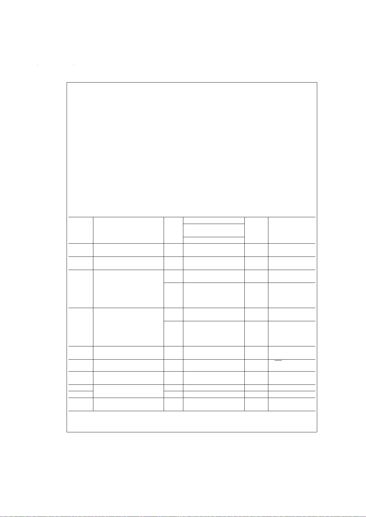
DC Electrical Characteristics for ’ACTQ Family Devices
54ACTQ
Symbol Parameter V
CC
T
A
=
Units Conditions
(V) −55˚C to +125˚C
Guaranteed Limits
V
IH
Minimum High Level 4.5 2.0 V V
OUT
=
0.1V
Input Voltage 5.5 2.0 or V
CC
− 0.1V
V
IL
Maximum Low Level 4.5 0.8 V V
OUT
=
0.1V
Input Voltage 5.5 0.8 or V
CC
− 0.1V
V
OH
Minimum High Level 4.5 4.4 V I
OUT
=
−50 µA
Output Voltage 5.5 5.4
(Note 3)
V
IN
=
V
IL
or V
IH
4.5 3.70 V IOH= −24 mA
5.5 4.70 I
OH
= −24 mA
V
OL
Maximum Low Level 4.5 0.1 V I
OUT
=
50 µA
Output Voltage 5.5 0.1
(Note 3)
V
IN
=
V
IL
or V
IH
4.5 0.50 V IOL=24mA
5.5 0.50 I
OL
=24mA
I
IN
Maximum Input 5.5
±
1.0 µA V
I
=
V
CC
, GND
Leakage Current
I
OZ
TRI-STATE Output Leakage
Current, High or Low
5.5
±
10.0 µA OE = 2.0V
I
CCT
Maximum 5.5 1.6 mA V
I
=
V
CC
− 2.1V
I
CC
/Input
I
OLD
Minimum Dynamic 5.5 50 mA V
OLD
=
1.65V Max
I
OHD
Output Current (Note 4) 5.5 −50 mA V
OHD
=
3.85V Min
I
CC
Maximum Quiescent 5.5 160.0 µA V
IN
=
V
CC
Supply Current or GND (Note 4)
www.national.com 2
 Loading...