100328
Low Power Octal ECL/TTL Bi-Directional Translator with
Latch
General Description
The 100328 is an octal latched bi-directional translator designed to convert TTL logic levels to 100K ECL logic levels
and vice versa.Thedirectionof this translation is determined
by the DIR input. A LOW on the output enable input (OE)
holds the ECL outputs in a cut-off state and the TTL outputs
at a high impedance level. A HIGH on the latch enable input
(LE) latches the data at both inputs even though only one
output is enabled at the time. A LOW on LE makes the
100328 transparent.
The cut-off state is designed to be more negative than a normal ECL LOW level. This allows the output emitter-followers
to turn off when the termination supply is −2.0V,presenting a
high impedance to the data bus. This high impedance reduces termination power and prevents loss of low state
noise margin when several loads share the bus.
The 100328 is designed with FAST
®
TTL output buffers, featuring optimal DC drive and capable of quickly charging and
discharging highly capacitive loads. All inputs have 50 kΩ
pull-down resistors.
Features
n Identical performance to the 100128 at 50%of the
supply current
n Bi-directional translation
n 2000V ESD protection
n Latched outputs
n FAST TTL outputs
n TRI-STATE
®
outputs
n Voltage compensated operating range
=
−4.2V to −5.7V
n Available to MIL-STD-883
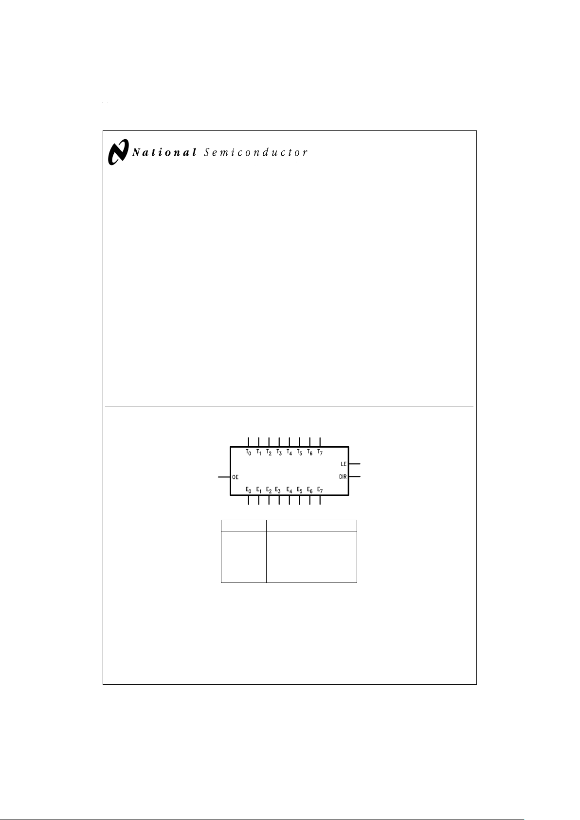
Logic Symbol
Pin Names Description
E
0–E7
ECL Data I/O
T
0–T7
TTL Data I/O
OE Output Enable Input
LE Latch Enable Input
DIR Direction Control Input
All pins function at 100K ECL levels except for T0–T7.
TRI-STATE®is a registered trademark of National Semiconductor Corporation.
FAST
®
is a registered trademark of Fairchild Semiconductor.
DS100295-1
August 1998
100328 Low Power Octal ECL/TTL Bi-Directional Translator with Latch
© 1998 National Semiconductor Corporation DS100295 www.national.com

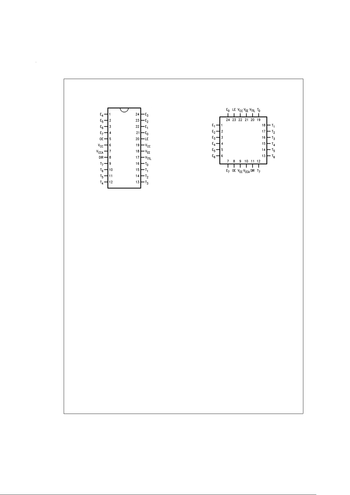
Connection Diagrams
24-Pin DIP
DS100295-2
24-Pin Quad Cerpak
DS100295-4
www.national.com 2

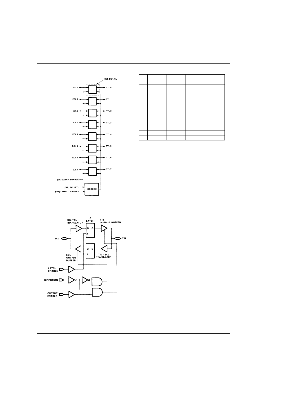
Functional Diagram
Detail
Truth Table
OE DIR LE ECL TTL Notes
Port Port
L X L LOW Z
(Cut-Off)
L L H Input Z (Notes 1, 3)
L H H LOW Input (Notes 2, 3)
(Cut-Off)
H L L L L (Notes 1, 4)
H L L H H (Notes 1, 4)
H L H X Latched (Notes 1, 3)
H H L L L (Notes 2, 4)
H H L H H (Notes 2, 4)
H H H Latched X (Notes 2, 4)
H=HIGH Voltage Level
L=LOW Voltage Level
X=Don’t Care
Z=High Impedance
Note 1: ECL input to TTL output mode.
Note 2: TTL input to ECL output mode.
Note 3: Retains data present before LE set HIGH.
Note 4: Latch is transparent.
DS100295-5
Note: LE, DIR, and OE use ECL logic levels
DS100295-6
www.national.com3

Absolute Maximum Ratings (Note 5)
If Military/Aerospace specified devices are required,
please contact the National Semiconductor Sales Office/
Distributors for availability and specifications.
Storage Temperature (T
STG
) −65˚C to +150˚C
Maximum Junction Temperature (T
J
)
Ceramic +175˚C
V
EE
Pin Potential to
Ground Pin −7.0V to +0.5V
V
TTL
Pin Potential to
Ground Pin −0.5V to +6.0V
ECL Input Voltage (DC) V
EE
to +0.5V
ECL Output Current
(DC Output HIGH) −50 mA
TTL Input Voltage (Note 7) −0.5V to +6.0V
TTL Input Current (Note 7) −30 mA to +5.0 mA
Voltage Applied to Output in HIGH State
TRI-STATE Output −0.5V to +5.5V
Current Applied to TTL
Output in LOW State (Max) Twice the Rated I
OL
(mA)
ESD (Note 6) ≥2000V
Recommended Operating
Conditions
Case Temperature (TC)
Military −55˚C to +125˚C
ECL Supply Voltage (V
EE
) −5.7V to −4.2V
TTL Supply Voltage (V
TTL
) +4.5V to +5.5V
Note 5: Absolute maximum ratings are those values beyond which the device may be damaged or have its useful life impaired. Functional operation
under these conditions is not implied.
Note 6: ESD testing conforms to MIL-STD-883, Method 3015.
Note 7: Either voltage limit or current limit is sufficient to protect inputs.
Military Version
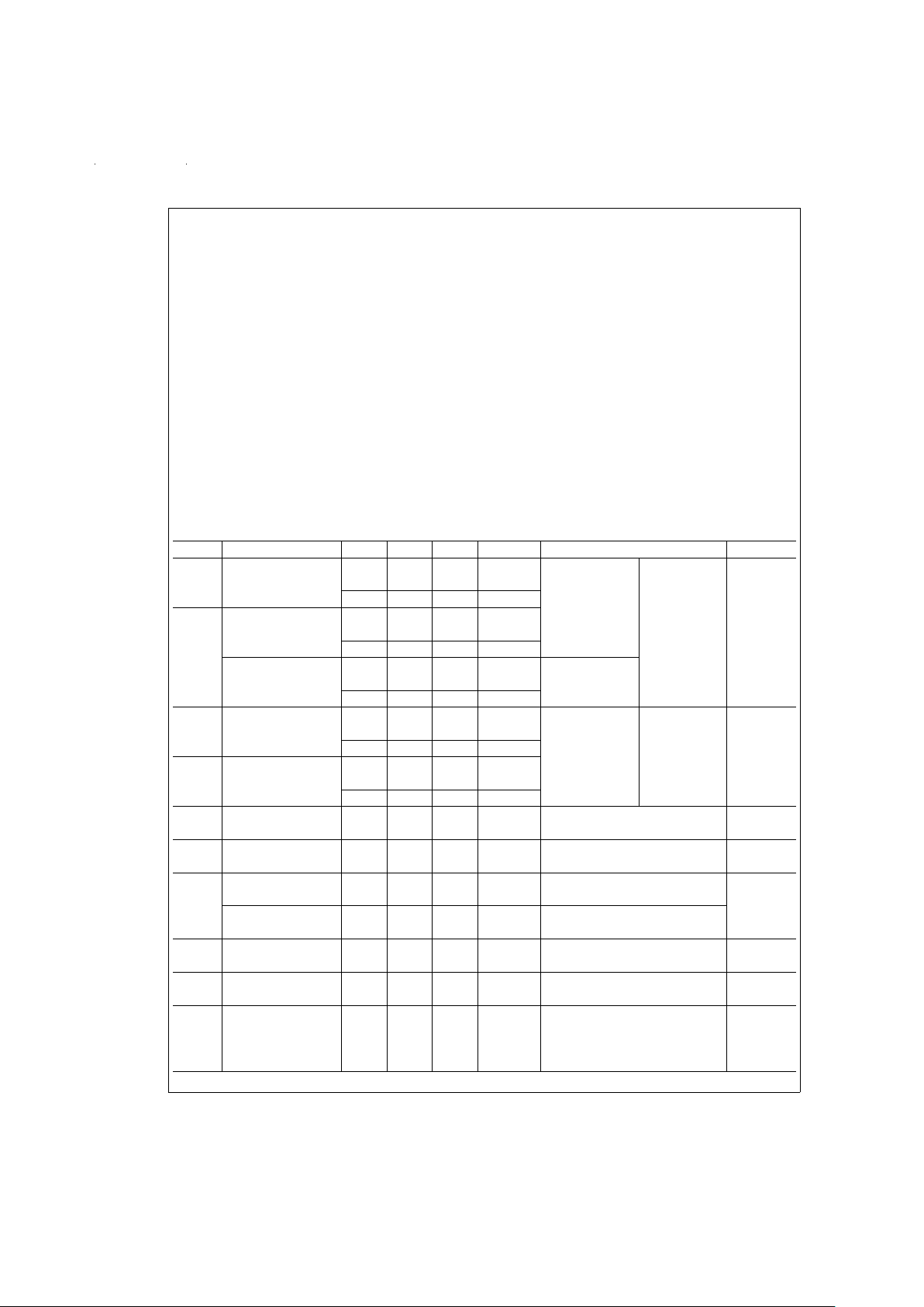
TTL-to-ECL DC Electrical Characteristics
V
EE
=
−4.2V to −5.7V, V
CC
=
V
CCA
=
GND, T
C
=
−55˚C to +125˚C, V
TTL
=
+4.5V to +5.5V
Symbol Parameter Min Max Units T
C
Conditions Notes
V
OH
Output HIGH Voltage −1025 −870 mV 0˚C to Loading with
50Ω to −2.0V
(Notes 8, 9,
10)
+125˚C
−1085 −870 mV −55˚C V
IN
=
V
IH
(Max)
V
OL
Output LOW Voltage −1830 −1620 mV 0˚C to or VIL(Min)
+125˚C
−1830 −1555 mV −55˚C
Cutoff Voltage −1950 mV 0˚C to
+125˚C OE or DIR Low
−1850 mV −55˚C
V
OHC
Output HIGH Voltage −1035 mV 0˚C to (Notes 8, 9,
10)
+125˚C
−1085 mV −55˚C V
IN
=
V
IH
(Min) Loading with
V
OLC
Output LOW Voltage −1610 mV 0˚C to or VIL(Max) 50Ω0 to −2.0V
+125˚C
−1555 mV −55˚C
V
IH
Input HIGH Voltage 2.0 V −55˚C to Over V
TTL,VEE,TC
Range (Notes 8, 9,
10, 11)
+125˚C
V
IL
Input LOW Voltage 0.8 V −55˚C to Over V
TTL,VEE,TC
Range (Notes 8, 9,
10, 11)
+125˚C
I
IH
Input HIGH Current 70 µA −55˚C to V
IN
=
+2.7V (Notes 8, 9,
10)
125˚C
Breakdown Test 1.0 mA −55˚C to V
IN
=
+5.5V
+125˚C
I
IL
Input LOW Current −1.0 mA −55˚C to V
IN
=
+0.5V (Notes 8, 9,
10)
+125˚C
V
FCD
Input Clamp −1.2 V −55˚C to I
IN
=
−18 mA (Notes 8, 9,
10)
Diode Voltage +125˚ C
I
EE
VEESupply Current LE Low, OE and DIR High (Notes 8, 9,
10)
−55˚C to Inputs Open
−165 −73 mA +125˚C V
EE
=
−4.2V to −4.8V
−175 −73 V
EE
=
−4.2V to −5.7V
www.national.com 4
 Loading...