
SM9403BM
NIPPON PRECISION CIRCUITS—1
NIPPON PRECISION CIRCUITS INC.
DVDRAM Servo-amplifier LSI
OVERVIEW
The SM9403BM is a DVDROM and DVDRAM servo preprocessor LSI, designed for double-speed format
DVDROM and DVDRAM drives.
The SM9403BM is fabricated using a BiCMOS process, and incorporates an analog signal processing circuit
that generates signals needed by the digital servo processor, a DPD signal processing circuit (DVDROM), and
a CAPA (Complementary Allocated Pit Address) detection circuit (DVDRAM) all in a single chip. It operates
from a single 5 V supply, and is available in 36-pin plastic SSOP packages.
FEATURES
■
DPD signal processor
■
Tracking error signal output
■
Focus error signal output
■
Tracking error signal sample-and-hold
■
Focus error signal sample-and-hold
■
CAPA detection function
■
Track count pulse generator
■
Off-track detection
■
2V and 4V reference voltage generator
■
Serial interface for setting internal parameters
■
Sleep-mode function
■
Single 5 V supply
■
36-pin plastic SSOP
APPLICATIONS
■
Double-speed DVDROM drives
■
Double-speed DVDRAM drives
ORDERING INFORMATION
PINOUT
36-pin SSOP (Top View)
De vice Pack ag e
SM9403BM 36-pin SSOP
1NC
2NC
3FER
4FHOLD
5FSUB
6ISET
7DPDD
8DPDC
9DPDB
10DPDA
11AGND
12MMTI
13CAPAN
14CAPAP
15CAPLFC
16TSUB
17THOLD
18TRE 19 VREF4
20 VREF2
21 TROFF
22 TRP
23 CAPAREA
24 CAPOUT
25 AVCC
26 CAPIN
27 CAPSEL
28 CAPSEEK
29 DVCC
30 SENB
31 SDATA
32 SCLK
33 DGND
34 DEFECT
35 DPDI
36 DPDG
SM9403BM
NPC
SM9403BM
NIPPON PRECISION CIRCUITS—2
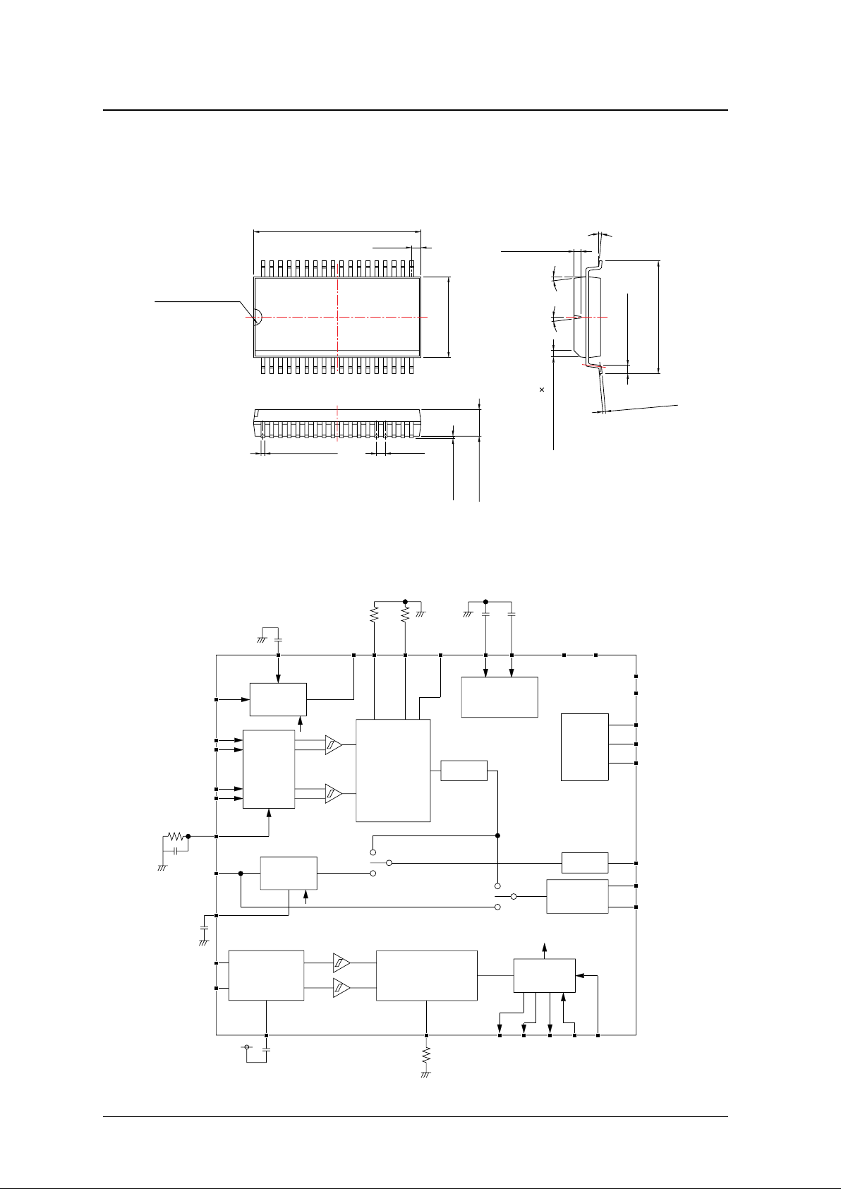
PACKAGE DIMENSIONS
(Unit: mm)
BLOCK DIAGRAM
2.44 to 2.64
0.85
15.20 to 15.40
7.40 to 7.60
0.29 to 0.39
0.80
0.10 to 0.30
0.51 to 1.01
10.11 to 10.51
0.63 ± 0.10
7°
0 to 8°
0.23 to 0.32
7°
0.51 ± 0.20 45°
R0.63 to 0.89
Phase
comparator
LPF
Voltage
reference
S / H
LPF
Serial
interface
S / H
control
DPDI
DPDG
ISET
VREF2
VREF4
FER
FHOLD
FSUB
TSUB
THOLD
CAPAP
CAPAN
CAPLFC
CAPIN
CAPOUT
CAPAREA
CAPSEL
CAPSEEK
TRP
TROFF
TRE
SENB
SDATA
SCLK
DGND
DVCC
AGND
AVCC
VREF2
DPDA
DPDB
DPDC
DPDD
Mono-multiviblator
Equalizer
Delay
LPF
Analog signal
processor
S / H
MMTI
SWB
Track Pulse
Generator
SWA
DEFECT
*
*
*

SM9403BM
NIPPON PRECISION CIRCUITS—3
PIN DESCRIPTION
Number Name I/O
1
1. I = input, Ipd = Input with built-in pull-down resistor, I/O = input/output (N-channel open-drain when output), O = output
Function
1 N C O No connection
2 N C O No connection
3 F E R O Focus error signal output
4 FHOLD – Focus error hold capacitor connection
5 FSUB I Focus error signal input
6 ISET I DPD signal equalizer, reference current set resistor connection
7 DPDD I DPD signal input D
8 DPDC I DPD signal input C
9 DPDB I DPD signal input B
10 D P DA I DPD signal input A
11 AG ND – Analog circuit ground
12 MMTI I Mono-multivibrator time-constant set resistor connection
13 C APAN I ID data signal differential inverting input
14 C APAP I ID data signal differential non-inver ting input
15 CAPLFC – Slice-level detect capacitor connection
16 TSUB I Tracking error signal input
17 THOLD – Tracking error hold capacitor connection
18 T R E O Tracking error signal output
19 VREF4 O 4V reference voltage output
20 VREF2 O 2V reference voltage output
21 TROF F O Off-trac k detect signal output. L OW when off-tra ck.
22 TRP O Track count pulse output. HIGH-level pulse for land to outer tracking.
23 CAPAREA O ID interval detect signal output. ID interval detected when HIGH.
24 CAPOUT O Outer offset ID detect signal output. Outer offset ID interval detected when HIGH.
25 AVCC – Analog circuit pow er supply
26 CAPIN O Inner offset ID detect signal output. Inner offset ID interval detected when HIGH.
27 CAPSEL Ipd ID interval signal input. ID interva l selected when HIGH.
28 CAPSEEK Ipd Seek operation signal input. Seek operation selected when HIGH.
29 DVC C – Logic circuit pow er supply
30 SENB I Serial interface enable input. Enabled when HIGH.
31 SDA TA I/O Serial interface data input/ackno wledge output
32 SCLK I Serial interface clock input
33 DGND – Logic circuit ground
34 DEFECT Ipd Defect position signal input. Defect position indicated when HIGH.
35 DPDI I DPD signal hold delay set resistor connection
36 DPDG I DPD signal phase difference to voltage converter coefficient set resistor connection
SM9403BM
NIPPON PRECISION CIRCUITS—4
SPECIFICATIONS
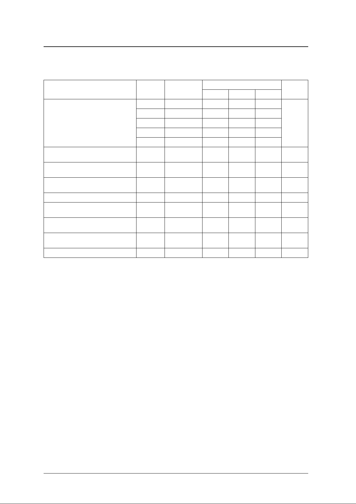
Absolute Maximum Ratings
GND = 0 V
Recommended Operating Conditions
GND = 0 V
Recommended External Components
Parameter Symbol Condition Rating Unit
Supply voltage range V
CC
−
0.5 to 7.0 V
Input voltage range V
IN
−
0.5 to VCC + 0.5 V
Operating temperature range T
opr
0 to 70
°
C
Storage temperature range T
stg
−
40 to 125
°
C
Po w er dissipation P
D
250 m W
Soldering temperature T
sld
260
°
C
Soldering time t
sld
10 s
Parameter Symbol Condition Rating Unit
Specifications supply voltage range V
CC
4.75 to 5.25 V
Operating supply voltage range V
CC
4.5 to 5.5 V
Operating temperature range T
opr
0 to 70
°
C
Pin No. Pin name Component Tolerance
4 FHOLD 1000pF capacitor K (±10%)
6 ISET
47kΩ resistor ± 1%
0.01µF capacitor Z (+80% to −20%)
12 MMTI 120kΩ resistor ± 1%
15 CAPLFC 0.01µF capacitor Z (+80% to −20%)
17 THOLD 1000pF capacitor K (±10%)
19 VREF4 0.1µF capacitor Z (+80% to −20%)
20 VREF2 0.1µF capacitor Z (+80% to −20%)
35 DPDI 47kΩ resistor ± 1%
36 DPDG 33k
Ω
resistor ± 1%
SM9403BM
NIPPON PRECISION CIRCUITS—5
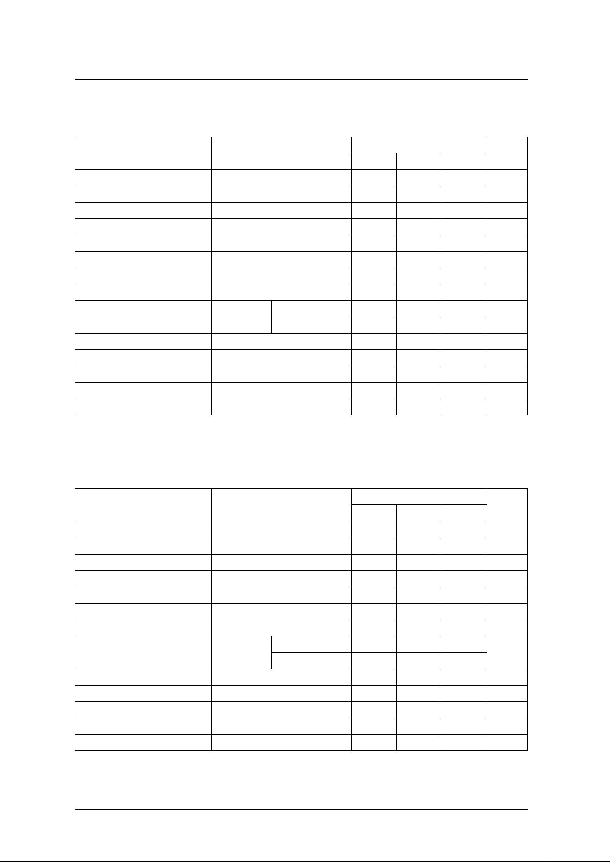
DC Electrical Characteristics
VCC = 5V ± 5%, GND = 0V, Ta = 0 to 70°C
Parameter Symbol Condition
Rating
Unit
min typ ma x
Current consumption
1
1. 33kΩ resistor connected between DPDG and AGN D 47kΩ resistor connected between DPDI and AGN D
120kΩ resistor connected between MMTI and AGN D 47kΩ resistor connected between ISET and AGN D
1000pF capacitor connected between FHOLD and AGN D 1000pF capacitor connected between THOLD and AG ND
0.1µF capacitor connected between VREF4 and AG ND 0.1µF capacitor connected between VREF2 and AG ND
0.01µF capacitor connected between CAPLFC and AGN D 0.01µF capacitor connected between ISET and AGN D
CA PAP, CAPAN, DPDA, DPDB, DPDC, DPDD, FSUB, TSUB connected to VREF2 or other 2V supply.
SENB, SDATA, SCLK connected to GND; All other pins (excluding supply and ground pins) open circuit.
Sleep mode 1: DPD system only in sleep condition.
Sleep mode 2: All block s except reference supply voltage generator in sleep condition.
Sleep mode 3: All blocks i n sleep condition.
I
CC1
Operating mode – 28 34
mA
I
CC2
Sleep mode 1 – 17 21
I
CC3
Sleep mode 2 – 2.0 2.6
I
CC4
Sleep mode 3 – – 1.0
∆
I
CCICC1
− I
CC2
9––
CAPSEEK, CAPSEL, DEFECT, SENB, SDATA,
SCLK HIGH-level input voltage
V
IH
0.8V
CC
––V
CAPSEEK, CAPSEL, DEFECT, SENB, SDATA,
SCLK LOW-level input voltage
V
IL
– – 0.2V
CC
V
CAPSEEK, CAPSEL, DEFECT HIGH-level input
current
I
IH1
VIN = V
CC
50 100 200 µ A
SENB, SDATA, SCLK HIGH-level input current I
IH2
VIN = V
CC
––3µA
CAPSEEK, CAPSEL, DEFECT, SENB, SDATA,
SCLK LOW-level input current
I
IL
VIN = GND
−
3– –µA
CA PAREA, CAPIN, CAPOUT, TR P, TROFF
HIGH-level output voltage
V
OHIOH
= −0.2mA VCC − 0.2 – – V
CA PAREA, CAPIN, CAPOUT, TR P, TROFF
L O W-level output voltage
V
OL1IOL
= 0.8mA – – 0.4 V
S D ATA L OW -level output voltage V
OL2IOL
= 7mA – – 1.0 V
SM9403BM
NIPPON PRECISION CIRCUITS—6
Focus Sample-and-Hold, Low-pass Filter Characteristics (FSUB → FER)
VCC = 5V ± 5%, GND = 0V, Ta = 0 to 70°C, FSUB and FER signals in phase
Tracking Sample-and-Hold, Low-pass Filter Characteristics (TSUB → TRE)
VCC = 5V ± 5%, GND = 0V, Ta = 0 to 70°C, TSUB and TRE signals in phase
Parameter Condition
Rating
Unit
min typ ma x
FSUB input signal range VREF2 reference
−
1.25 0 +1.25 V
FER output voltage range VREF2 reference
−
1.25 0 +1.25 V
FER output offset voltage VREF2 reference, VIN = V
REF2
– – ±8.0 m V
FER output offset voltage temperature drift VREF2 reference – – ±45 µV/°C
FER output signal slew rate LPF off 1 – – V/µs
FER output load regulation I
OUT
= ±3mA, VIN = V
REF2
– – ±10 mV
FSUB input impedance 100 – – k
Ω
FER output signal gain
−
0.17 0 +0.17 dB
FER output signal bandwidth
1
1. CL = 20pF, RL = 500
Ω
VIN = 1.5Vp-p,
−
3dB from DC
LPF off (FFE = HIGH) 500 – –
kHz
LPF on (FFE = LOW) 11 5 160 23 0
FER output gain peaking
1
DC to −3dB frequency
−
3 – +0.5 dB
Hold time FER output droop characteristic VIN = 200mVp-p, C
FHOLD
= 1000pF – – 0.025 %/µs
S/H acquisition time
∆
VIN = 200mV, target value ± 10% – – 1 µs
FER output hold error With respect to the previous value – – ±4 mV
Pow er-down state FER output impedance 1 – – M
Ω
Parameter Condition
Rating
Unit
min typ ma x
TSUB input signal range VREF2 reference
−
1.25 0 +1.25 V
TRE output voltage range VREF2 reference
−
1.25 0 +1.25 V
TRE output offset voltage VREF2 reference, VIN = V
REF2
– – ±8.0 m V
TRE output offset voltage temperature drift VREF2 reference – – ±45 µV/
°
C
TRE output load regulation I
OUT
= ±3mA, VIN = V
REF2
– – ±10 mV
TSUB input impedance 100 – – k
Ω
TRE output signal gain
−
0.17 0 +0.17 dB
TRE output signal bandwidth
1
1. CL = 20pF, RL = 500
Ω
VIN = 1.5Vp-p,
−
3dB from DC
TFE = HIGH 24 35 50
kHz
TFE = LOW 115 160 230
TRE output gain peaking
1
DC to −3dB frequency
−
3 – +0.5 dB
Hold time TRE output droop characteristic VIN = 200mVp-p, C
THOLD
= 1000pF – – 0.025 %/µs
S/H acquisition time
∆
VIN = 200mV, target value ±10% – – 1 µs
TRE output hold error With respect to the previous value – – ±4 mV
Power-down state TRE output impedance 1 – – M
Ω
 Loading...