NPC SM8580AM Datasheet
−
SM8580AM
Real-time Clock IC with 4-bit Interface
NIPPON PRECISION CIRCUITS INC.
OVERVIEW
The SM8580AM is a real-time clock IC based on a 32.768 kHz crystal oscillator, which features a 4-bit parallel interface for communication with an external microcontroller.
It comprises second-counter to year-counter clock and calendar circuits that feature automatic leap-year adjustment up to year 2099, alarm and timer interrupt functions, clock counter change detect functions, ±30-second
correction function, time error correction function, and built-in temperature sensor.
The 4-bit parallel interface is compatible with general-purpose SRAM over a high-speed bus.
and Built-in Temperature Sensor
FEATURES
■
High-speed bus 4-bit parallel interface
■
Date, day, hour, minute, and second-counter presettable alarm interrupt
■
1/4096 seconds to 255 minutes presettable interval
timer interrupt function
■
2 software-maskable alarm and timer interrupt
outputs
■
Clock counter change detect functions
■
4-digit western calendar display
■
Automatic leap year correction up to year 2099
■
±30-second adjust function
■
195 to +192ppm time error correction range
■
Built-in temperature sensor (analog voltage output)
■
2.4 to 5.5V interface voltage range
■
1.6 to 5.5V clock voltage range
■
0.6µA/3V (typ) current consumption
ORDERING INFORMATION
De vice Pack ag e
SM8580AM 24-pin SSOP
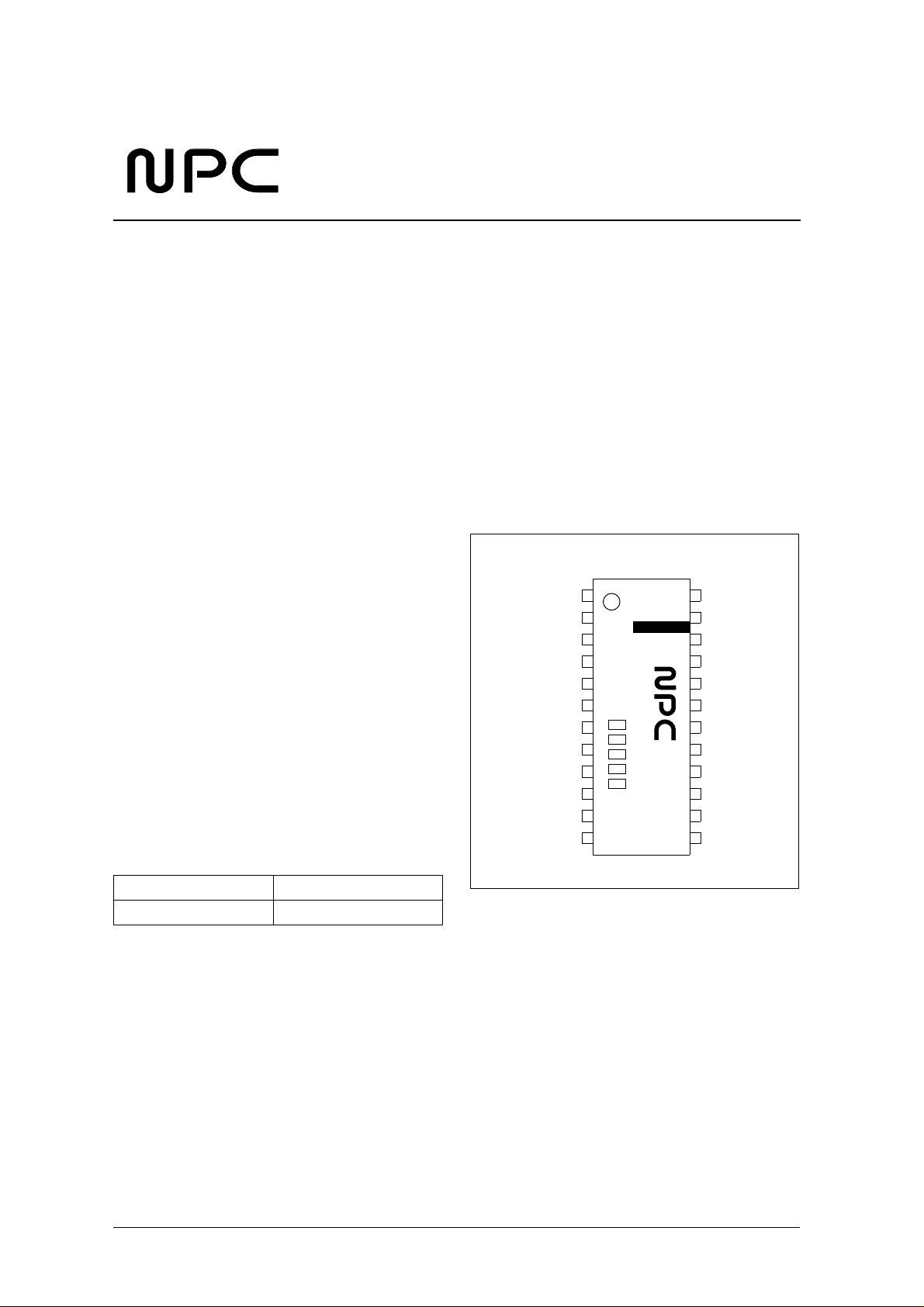
PINOUT
(Top view)
CE0N
FCON
FOUT
VTEMP
AIRQN
TIRQN
A0
A1
A2
A3
RDN
VSS
1
SM8580AM
12
24
VDD
XT
XTN
N.C.
N.C.
N.C.
CE1
D0
D1
D2
D3
13
WRN
NIPPON PRECISION CIRCUITS—1
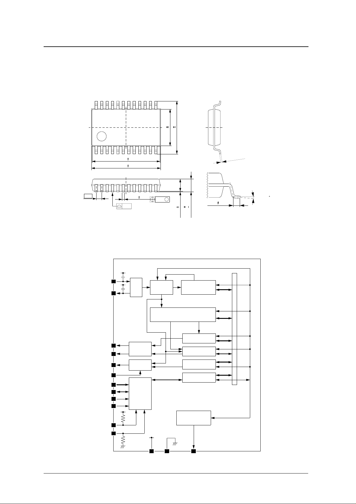
PACKAGE DIMENSIONS
(Unit: mm)
24-pin SSOP
10.05 0.20
10.20 0.30
SM8580AM
7.80 0.30
5.40 0.20
0.15
+
−
0.1
0.05
0.8
BLOCK DIAGRAM
XTN
AIRQN
TIRQN
FOUT
FCON
A0 to A3
D0 to D3
WRN
RDN
CE0N
XT
CE1
0.36 0.10
0.10
CG
CD
OSC
Interrupt
Control
FOUT
Control
BUS
Interface
M
0.12
Divider
Clock and Calendar
1.80
0.10
0.20
1.90
0.10 0.10
Digital Trimming
Controller
Counter
Alarm Register
Timer Register
FOUT Register
Control Register
Temperature
Sensor
0.50 0.20
Control line
0 to 10
VDD VSS
VTEMP
NIPPON PRECISION CIRCUITS—2
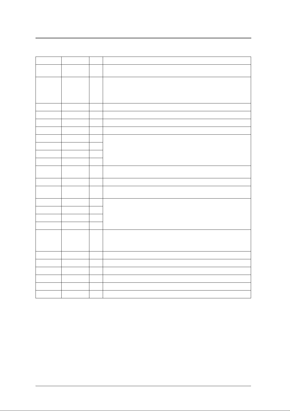
PIN DESCRIPTION
SM8580AM
Number Name I/O Function
1 CE0N I
2 FCON I
3 FOUT O Frequency set register, frequency output (CMOS output)
4 VTEMP O Temperature voltage output (analog output)
5 AIRQN O Alarm interrupt output (N-channel open-drain output)
6 TIRQN O Timer interrupt output (N-channel open-drain output)
7A0I
8A1I
9A2I
10 A3 I
11 RDN I
12 VS S – Ground
13 WRN I
14 D 3 I/O
15 D 2 I/O
16 D 1 I/O
17 D 0 I/O
18 CE1 I
19 NC – No connection
20 NC – No connection
21 NC – No connection
22 X T N O Oscillator output, with built-in oscillator capacitance C
23 XT I Oscillator output, with built-in oscillator capacitance C
24 V D D – Supply
1. Connect a 0.1µF capacitor between VDD and VS S.
Chip enable 0 input with built-in pull-up resistor.
The SM8580AM can be accessed when CE0N is LOW and CE1 is HIGH.
FOUT output frequency select control input (when CE1 is HIGH).
32.768kHz fixed frequency output when FCON is LOW.
Output frequency determined by bit FD when FCON is HIGH (when FE bit is 1).
Note that a HIGH-level voltage should be applied to FCON to avoid unwanted 32.768kHz output during
backup.
Address inputs.
Connect to the microcontroller address bus.
The selected register address is input on this bus when accessing the SM8580AM (positive logic).
Read strobe input. Data can be read from SM8580AM when RDN is LOW and WRN is HIGH.
An error will occur if both RDN and WRN are simultaneously LOW.
W rite strobe input. Data can be written to SM8580AM when RDN is HIGH and WRN is LOW.
An error will occur if both RDN and WRN are simultaneously LOW.
Data bus input/outputs.
Connect to the microcontroller data bus.
Chip enable 1 input with built-in pull-down resistor.
The SM8580AM can be accessed when CE0N is LOW and CE1 is HIGH.
FOUT is in output mode when CE1 is HIGH, regardless of the state of CE0N. FOUT is high impedance
when CE1 is LOW.
1
D
G
NIPPON PRECISION CIRCUITS—3
−
−
−
−
−
° C
−
°
SM8580AM
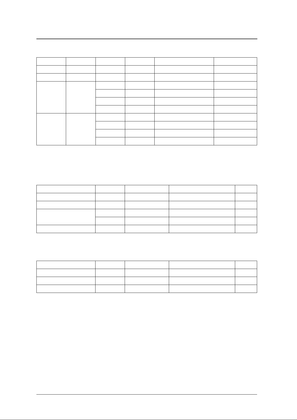
FOUT Output and SM8580AM Access Relationship
CE0N CE1 FCON FE bit FOUT output SM8580AM accessible
HIGH L OW
LOW LOW
HIGH HIGH
LOW HIGH
××
××
High impedance No
High impedance No
LO W 0 32.768kHz output No
LO W 1 32.768kHz output No
HIGH 0 High impedance No
HIGH 1 FD bit select frequency output No
LO W 0 32.768kHz output Yes
LO W 1 32.768kHz output Yes
HIGH 0 High impedance Yes
HIGH 1 FD bit select frequency output Yes
SPECIFICATIONS
Absolute Maximum Ratings
V
= 0 V
SS
Parameter Symbol Condition Rating Unit
Supply voltage range V
Input voltage range V
Output voltage range
Storage temperature range T
Recommended Operating Conditions
V
= 0 V
SS
Parameter Symbol Condition Rating Unit
Supply voltage range V
Clock supply voltage range V
Operating temperature range T
V
OUT1
V
OUT2
DD
IN
stg
DD
CLK
opr
All inputs, D0 to D3 V
TIRQN, AIRQN V
FOUT, D0 to D3, VTEMP V
0.3 to 7.0 V
SS
SS
0.3 to V
SS
0.3 to V
+ 0.3 V
DD
0.3 to 8.0 V
+ 0.3 V
DD
55 to 125
2.4 to 5.5 V
1.6 to 5.5 V
40 to 85
C
NIPPON PRECISION CIRCUITS—4
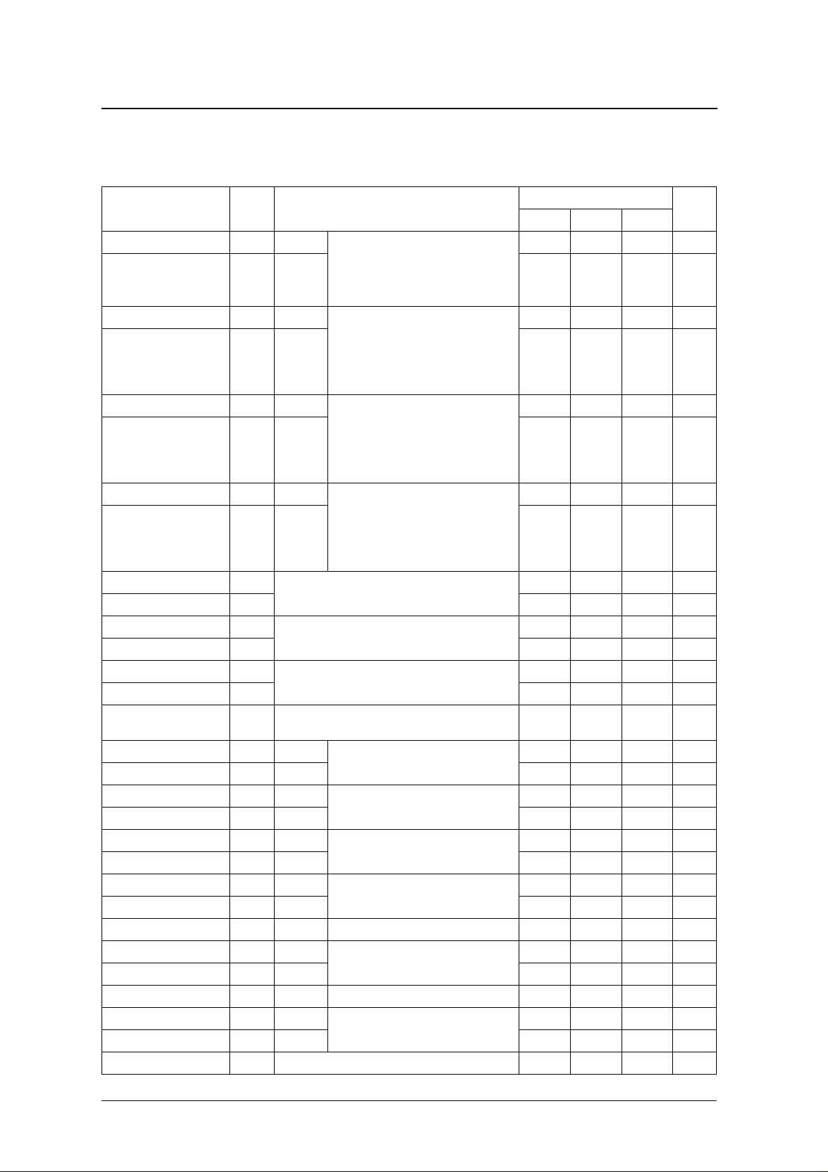
DC Electrical Characteristics
−
−
−
V
= 0V, V
SS
= 1.6 to 5.5V, T
DD
= − 40 to 85 ° C unless otherwise noted
a
SM8580AM
°
−
−
Parameter Symbol Condition
Current consumption 1 I
DD1
V
= 5V CE0N = RDN = WRN = V
DD
A0 to A3 = D0 to D3 = V
CE1 = FCON = V
Current consumption 2 I
DD2
V
= 3V – 0.6 1.0 µA
DD
AIRQN = TIRQN = FOUT = V
VTEMP output OFF (TEMP bit = 0)
Current consumption 3 I
DD3
V
= 5V Ta = 25
DD
CE0N = RDN = WRN = V
A0 to A3 = D0 to D3 = V
Current consumption 4 I
DD4
V
DD
CE1 = FCON = V
= 3V – 40 6 0 µA
AIRQN = TIRQN = FOUT = V
VTEMP output ON (TEMP bit = 1)
Current consumption 5 I
DD5
V
= 5V CE0N = CE1 = RDN = WRN = V
DD
A0 to A3 = D0 to D3 = V
FCON = V
Current consumption 6 I
DD6
V
DD
AIRQN = TIRQN = FOUT = VTEMP = Hi-Z,
= 3V – 1.7 4.5 µA
VTEMP output OFF (TEMP bit = 0),
FOUT = 32kHz output, C
Current consumption 7 I
DD7
V
= 5V CE0N = CE1 = RDN = WRN = V
DD
A0 to A3 = D0 to D3 = V
FCON = V
Current consumption 8 I
DD8
V
DD
AIRQN = TIRQN = FOUT = VTEMP = Hi-Z,
= 3V – 5.0 12 µ A
VTEMP output OFF (TEMP bit = 0),
FOUT = 32kHz output, C
HIGH-level input voltage 1 V
L O W -level input voltage 1 V
HIGH-level input voltage 2 V
L O W -level input voltage 2 V
HIGH-level input voltage 3 V
L O W -level input voltage 3 V
Input leakage current I
Pull-up resistance 1 R
Pull-up resistance 2 R
Pull-down resistance 1 R
Pull-down resistance 2 R
Pull-down resistance 3 R
Pull-down resistance 4 R
HIGH-level output voltage 1 V
HIGH-level output voltage 2 V
HIGH-level output voltage 3 V
L O W-level output voltage 1 V
L O W-level output voltage 2 V
L O W-level output voltage 3 V
L O W-level output voltage 4 V
L O W-level output voltage 5 V
Output leakage current I
IH1
V
= 4.5 to 5.5V,
DD
CE0N, FCON, RDN, WRN, A0 to A3, D0 to D3
IL1
IH2
V
= 2.4 to 3.6V,
DD
CE0N, FCON, RDN, WRN, A0 to A3, D0 to D3
IL2
IH3
V
= 1.6 to 5.5V,
DD
CE1
IL3
CE0N = V
LEAK
FCON = RDN = WRN = A0 to A3 = V
V
UP1
DD
V
UP2
DD
V
DWN1
DD
V
DWN2
DD
V
DWN3
DD
V
DWN4
DD
V
OH1
DD
V
OH2
DD
V
OH3
DD
V
OL1
DD
V
OL2
DD
V
OL3
DD
V
OL4
DD
V
OL5
DD
D0 to D3, AIRQN, TIRQN, FOUT, V
OZ
, CE1 = V
DD
= 5V
CE0N = V
= 3V 150 300 600 k Ω
= 5V
CE1 = V
= 3V 42.5 85 17 0 M Ω
= 5V
CE1 = 0.5V
= 3V 55 110 220 k Ω
= 5V
I
OH
= 3V 2.0 – 3.0 V
= 3V I
OH
= 5V
I
OL
= 3V 0 – 0.8 V
= 3V I
OL
= 5V
I
OL
= 3V 0 – 0.4 V
Rating
Unit
+ 0.3 V
+ 0.3 V
DD
+ 0.3 V
DD
C,
SS
SS
SS
min typ max
SS
,
DD
or V
,
DD
DD
SS
,
,
– 1.0 2.0 µA
–5075µA
,
DD
or V
,
DD
,
SS
= 0pF
L
,
SS
= 30pF
L
or V
DD
DD
SS
SS
,
DD
DD
,
,
– 3.0 7.5 µA
– 8.0 20 µ A
2.2 – V
V
0.3 – 0.8 V
SS
0.8V
DD
V
0.3 – 0.2V
SS
0.8V
DD
V
0.3 – 0.2V
SS
DD
–V
DD
–V
DD
0.5 – 0.5 µA
,
SS
,
,
,
75 150 300 k Ω
SS
20 40 80 M Ω
DD
30 60 120 k Ω
4.5 – 5.0 V
= − 1mA, D0 to D3, FOUT
= − 100µA, D0 to D3, FOUT 2.9 – 3.0 V
0 – 0.5 V
= 1mA, D0 to D3, FOUT
= 100µA, D0 to D3, FOUT 0 – 0.1 V
0 – 0.25 V
= 1mA, AIRQN, TIRQN
= V
OUT
DD
or V
SS
0.5 – 0.5 µA
V
V
NIPPON PRECISION CIRCUITS—5
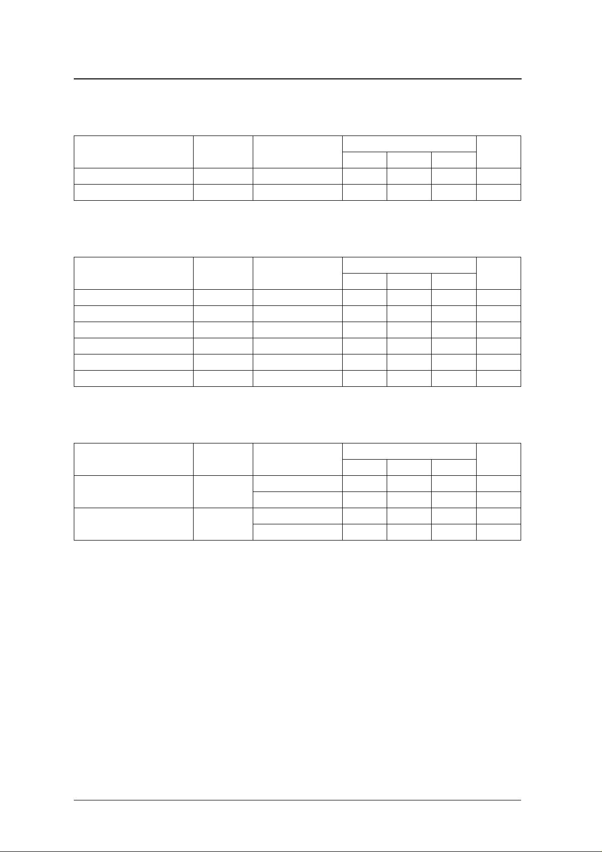
Terminal Capacitance Characteristics
Ta = 25°C, f = 1MHz
SM8580AM
Parameter Symbol Condition
Address input capacitance C
Data output capacitance C
ADD
DATA
min typ max
A0 to A3 – – 8 pF
D0 to D3 – – 15 pF
Rating
Oscillator Characteristics
Ta = 25°C, Seiko Epson C-002SH crystal (CI = 30kΩ, CL = 10pF) unless otherwise noted
Parameter Symbol Condition
Oscillator start time t
Oscillator stop voltage V
Frequency voltage characteristic f/V VDD = 1.6 to 5.5V
Frequency accuracy
Input capacitance C
Output capacitance C
STA
STO
ε
IC
G
D
VDD = 1.6 V – – 3. 0 s
VDD = 3.0V
VDD = 3.0V – 15 – pF
VDD = 3.0V – 10 – pF
min typ max
– – 1.5 V
−
2 – +2 ppm/V
−
20 – +20 ppm
Rating
AC Characteristics (1)
VSS = 0V, Ta = −40 to 85°C unless otherwise noted
Unit
Unit
Parameter Symbol Condition
FOUT duty Duty
Oscillator failure detection time t
OSC
Rating
Unit
min m ax min
VDD = 5V ± 10% 40 – 60 %
VDD = 3V ± 10% 40 – 60 %
VDD = 5V ± 10% 10 – – ms
VDD = 3V ± 10% 10 – – ms
NIPPON PRECISION CIRCUITS—6
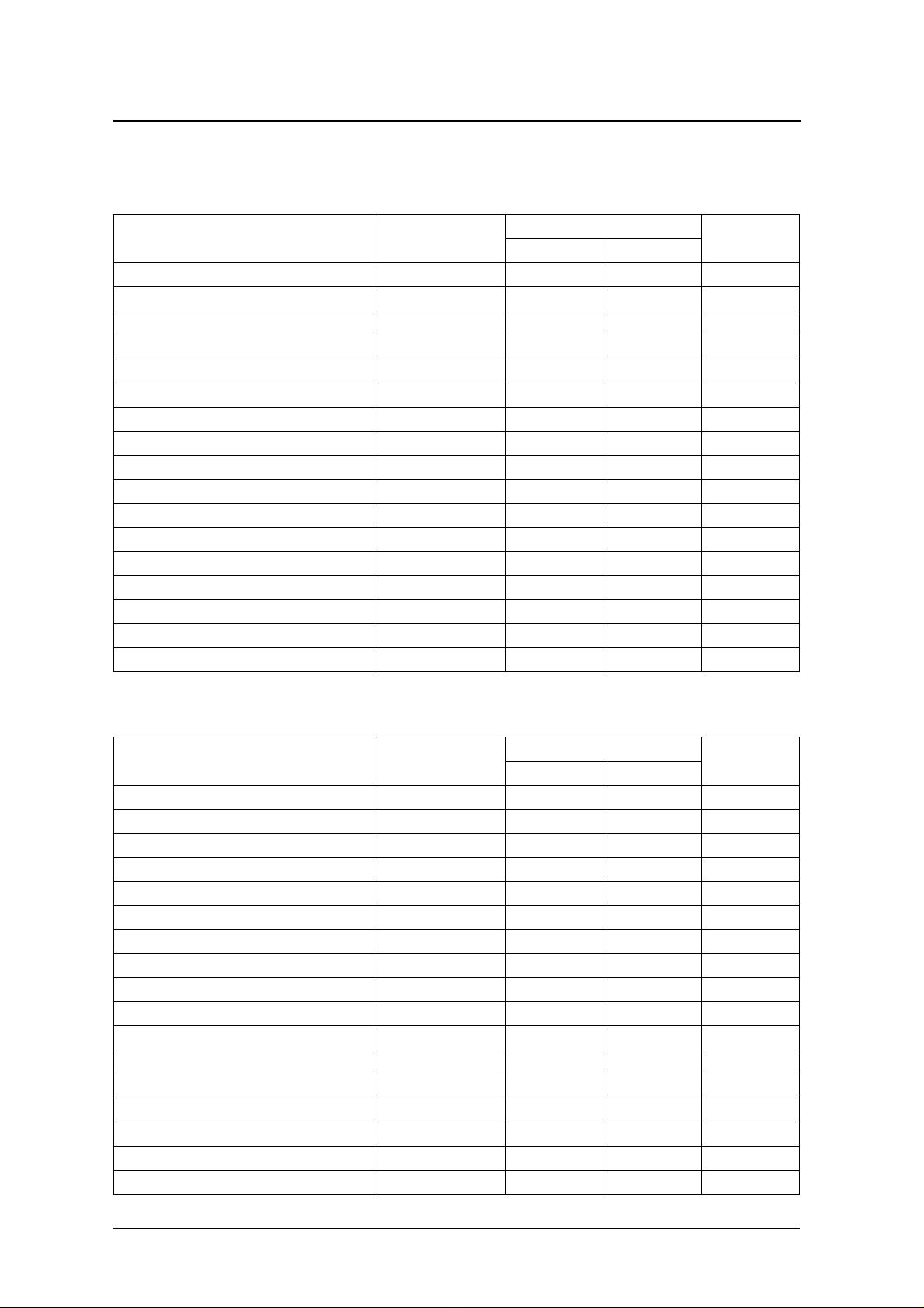
AC Characteristics (2)
SM8580AM
VDD = 2.4 to 3.6V, VSS = 0V, Ta = −40 to 85°C, inputs VI = 0.5VDD, outputs VO = 0.5V
output load capacitance CL = 100pF (t
Parameter Symbol
Read cycle time t
Address access time t
CE access time t
RD access time t
CE output set time t
CE output floating t
RD output set time t
RD output floating t
Output hold time t
W r ite cycle time t
Chip select time t
Address valid to end-of-write t
Address setup time t
Address hold time t
W r ite pulsewidth t
Input data set time t
Input data hold time t
ACC
, t
, t
ARD
)
ACS
Rating
min max
RC
ACC
ACS
ARD
CLZ
CHZ
OLZ
OHZ
OH
WC
CW
AW
AS
WR
WP
DW
DH
150 – ns
– 150 ns
– 150 ns
– 100 ns
5–ns
–60ns
5–ns
–60ns
10 – ns
150 – ns
140 – ns
140 – ns
0–ns
0–ns
130 – ns
80 – ns
0–ns
DD
Unit
VDD = 4.5 to 5.5V, VSS = 0V, Ta = −40 to 85°C, inputs VI = 0.5VDD, outputs VO = 0.5V
output load capacitance CL = 100pF (t
Parameter Symbol
Read cycle time t
Address access time t
CE access time t
RD access time t
CE output set time t
CE output floating t
RD output set time t
RD output floating t
Output hold time t
W r ite cycle time t
Chip select time t
Address valid to end-of-write t
Address setup time t
Address hold time t
W r ite pulsewidth t
Input data set time t
Input data hold time t
ACC
, t
, t
ARD
)
ACS
Rating
min max
RC
ACC
ACS
ARD
CLZ
CHZ
OLZ
OHZ
OH
WC
CW
AW
AS
WR
WP
DW
DH
85 – ns
–85ns
–85ns
–45ns
3–ns
–30ns
3–ns
–30ns
5–ns
85 – ns
70 – ns
70 – ns
0–ns
0–ns
65 – ns
35 – ns
0–ns
DD
Unit
NIPPON PRECISION CIRCUITS—7
 Loading...