NPC SM8578BV Datasheet

❏
SM8578BV
NIPPON PRECISION CIRCUITS INC.
OVERVIEW
The SM8578BV is a CMOS serial interface, realtime clock IC that uses a 32.768 kHz crystal oscillator for its reference timing.
It comprises second-counter to year-counter clock
and calendar circuits that feature automatic leap-year
adjustment, alarm and timer interrupt functions, as
well as oscillator stop, timer reloading, and other
detection functions. Data is transferred to and from
an external controller using a 3-wire serial interface.
It is available in compact 8-pin VSOP packages,
making it ideal for use in all types of portable, handheld equipment.
FEATURES
■
3-wire serial interface control
■
Day (day of the month), weekday (Sunday to Saturday), hour and minute alarm interrupt function
■
1/4096 seconds to 255 minutes presettable interval
timer interrupt function
■
Oscillator stop and timer reload detect functions
■
Automatic leap-year adjustment function (W estern
and Japanese calendars)
■
1.6 to 5.5 V supply voltage range
■
0.5 µA (typ. at 3 V) current consumption
■
C
oscillator capacitor built-in
D
■
Compact 8-pin VSOP package
Real-time Clock IC
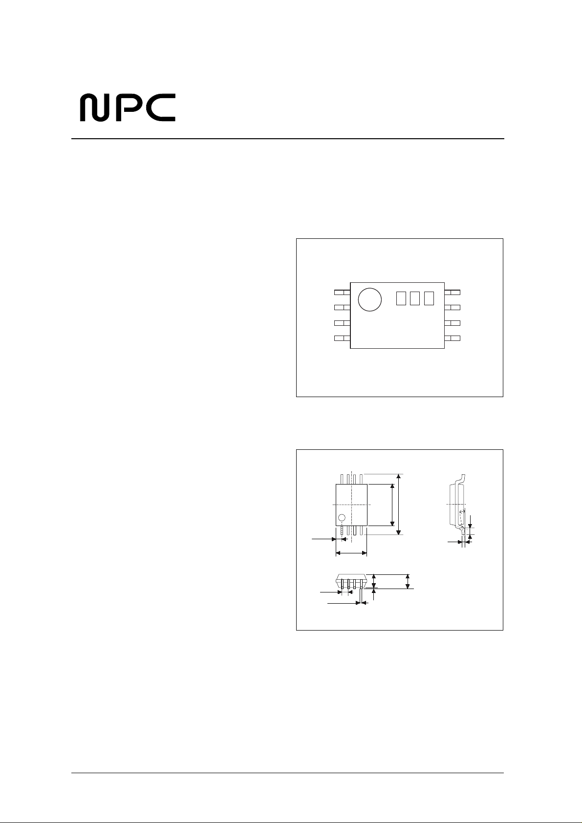
PINOUT
8-pin VSOP
Top view
INTN
XTN
XT
VSS
= date code
PACKAGE DIMENSIONS
Unit: mm
0.585 TYP
1
8578B
4
4.4±0.2
3.12±0.3
6.4±0.3
0.15
8
VDD
DATA
CLK
CE
5
0 to 10°
0.5±0.2
+0.1
-0.05
0.65
0.22±0.1
1.15±0.05
0.05±0.05
NIPPON PRECISION CIRCUITS—1
1.30 MAX

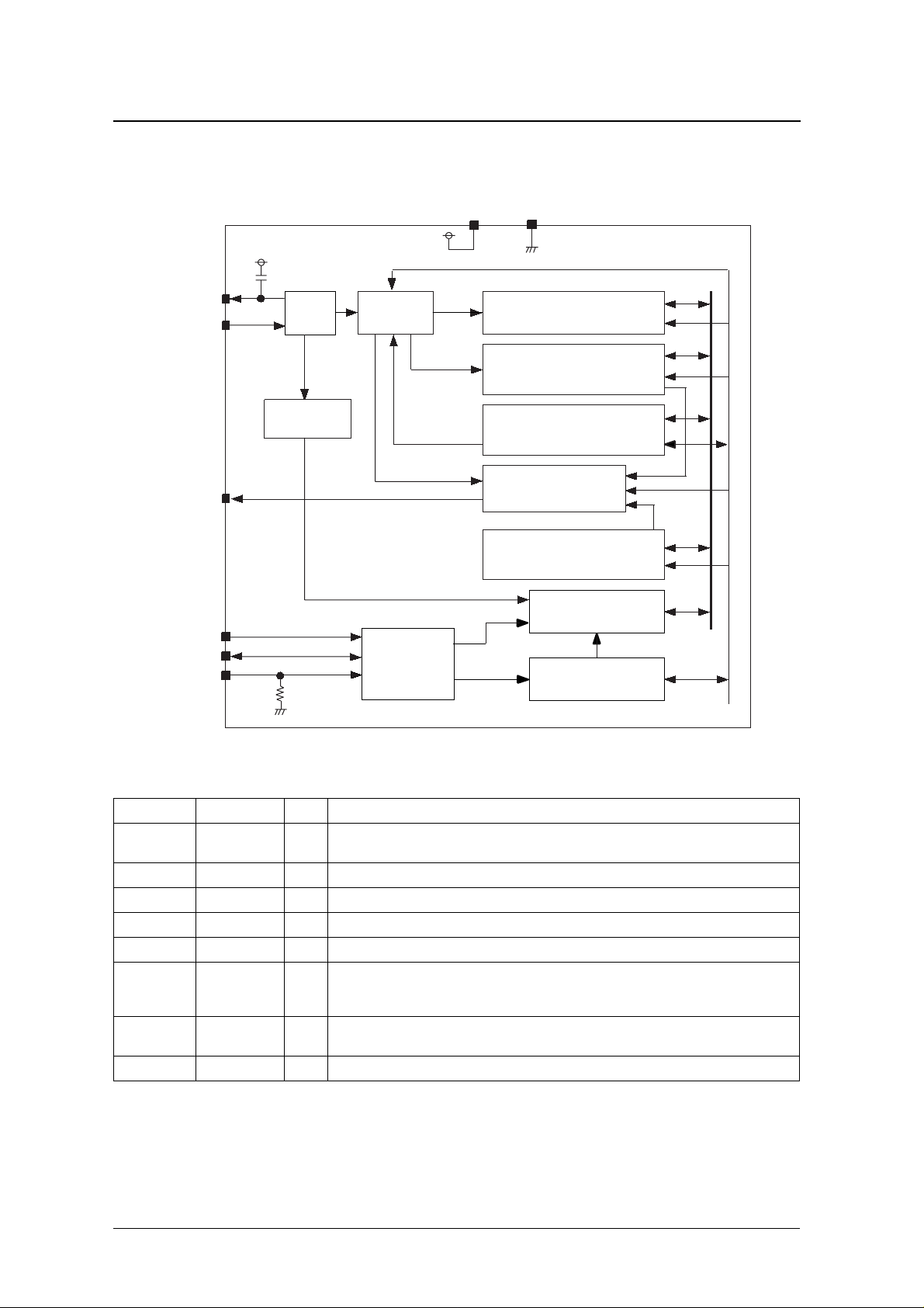
BLOCK DIAGRAM
SM8578BV
XTN
XT
INTN
CLK
DATA
CE
C
D
DETECT
OSC
OSC
DIVIDER
INPUT
CONTROLLER
VDD
INTERRUPT and FOUT
VSS
Control Line
CLOCK and CALENDAR
REGISTER
DIVIDER and
TIMER COUNTER
CONTROL REGISTER
CONTROLLER
ALARM REGISTER
SHIFT REGISTER
Internal Bus
CONTROL CIRCUIT
PIN DESCRIPTION
Number Name I/O Function
1 INTN O
2 XTN O Oscillator output. Oscillator capacitor C
3 XT I Oscillator input
4 VSS – Negative supply pin
5 CE I Chip enable. Chip is selected when HIGH. Pull-down resistor built-in
6 CLK I
7 DATA I/O
8 VDD – Positive supply voltage. A 0.1 µF pass capacitor should be connected between VDD and VSS.
Timer/alarm interrupt output and the setting frequency output,corresponding to the active internal mode.
N-channel open-drain output pin
built-in
D
Serial data clock.
In write mode, data is input on DATA on the rising edge of CLK.
In read mode, data is output on DATA on the rising edge of CLK.
Serial data input/output. When CE goes HIGH, initial 4-bit input data determines the device mode.
Subsequent data is transferred in write or read mode, as selected by the de vice mode.
NIPPON PRECISION CIRCUITS—2

−
−
−
−
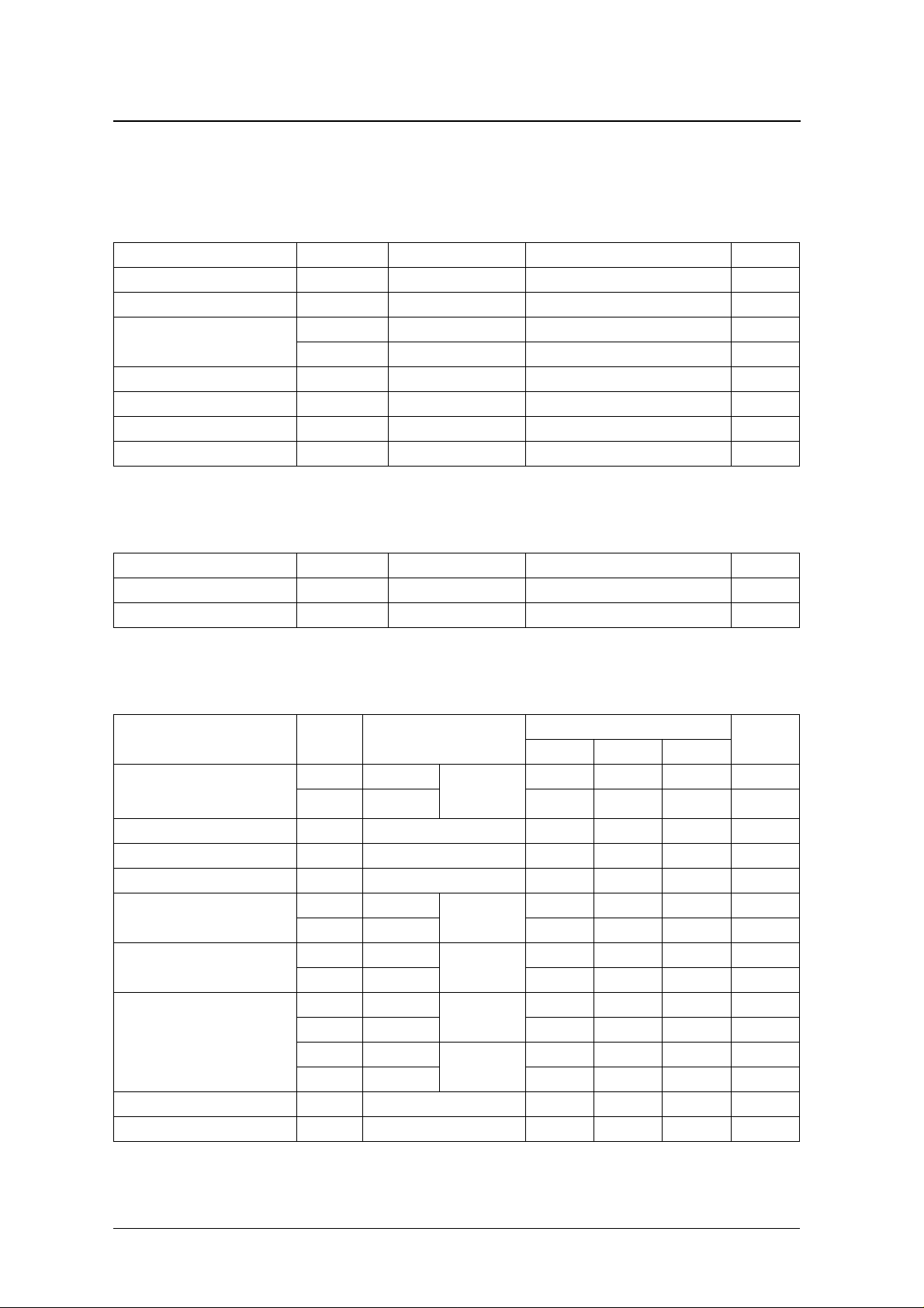
SPECIFICATIONS
Absolute Maximum Ratings
V
= 0 V
SS
Parameter Symbol Condition Rating Unit
Supply voltage range V
Input voltage range V
Output voltage range
Power dissipation P
Storage temperature range T
Soldering temperature T
Soldering time t
V
V
DD
OUT1
OUT2
STG
SLD
SLD
−
°
°
−
° C
−
SM8578BV
0.3 to 7.0 V
IN
All inputs V
INTN V
DATA V
D
SS
SS
0.3 to V
SS
0.3 to V
+ 0.3 V
DD
0.3 to 8.0 V
+ 0.3 V
DD
150 mW
55 to 125
255
10 s
C
C
Recommended Operating Conditions
V
= 0 V
SS
Parameter Symbol Condition Rating Unit
Supply voltage range V
Operating temperature range T
DD
opr
DC Electrical Characteristics
V
= 0 V, V
SS
Current consumption
HIGH-level input voltage V
LOW-level input voltage V
Input leakage current I
Input resistance
HIGH-level output voltage
LOW-level output voltage
Output leakage current I
Oscillator stop detection time t
= 1.6 to 5.5V , C
DD
= 10 pF, T
G
= − 40 to 85 ° C unless otherwise noted
a
Parameter Symbol Condition
I
I
LEAK
R
DWN1
R
DWN2
V
V
V
V
V
V
OSC
DD1
DD2
OH1
OH2
OL1
OL2
OL3
OL4
OZ
V
= 5.0 V CE = V
DD
V
= 3.0 V – 0.5 1.0 µA
DD
CE, CLK, DATA 0.8V
IH
CE, CLK, DATA 0 – 0.2V
IL
CE, CLK: V
V
= 5.0 V
DD
V
= 3.0 V 150 300 600 k Ω
DD
V
= 5.0 V
DD
V
= 3.0 V 2.0 – 3.0 V
DD
V
= 5.0 V
DD
V
= 3.0 V – – V
DD
V
= 5.0 V
DD
V
= 3.0 V – – V
DD
DATA, INTN: V
DATA, INTN =
V
DD
= V
IN
DD
CE: V
DATA: I
mA
DATA: I
mA
INTN: I
mA
OUT
= V
or V
IN
DD
OL
SS
SS
= V
OH
OL
= − 1
= 1
= 1
or V
DD
1.6 to 5.5 V
40 to 85
Rating
min typ m ax
– 1.0 2.0 µA
DD
–V
-0.5 – 0.5 µA
75 150 300 k Ω
4.5 – 5.0 V
––V
––V
SS
0.5 – 0.5 µA
10 – – ms
DD
DD
+ 0.5 V
SS
+ 0.8 V
SS
+ 0.25 V
SS
+ 0.4 V
SS
Unit
V
V
NIPPON PRECISION CIRCUITS—3

Oscillator Characteristics
T
= 25 ° C, C
a
= 10 pF, Seiko Epson C-002SH crystal (C
G
SM8578BV
= 30 k Ω , C
I
= 6 pF) unless otherwise noted
L
−
−
Parameter Symbol Condition
Oscillator start time t
Oscillator stop voltage V
STA
STO
Frequency voltage characteristic f/V V
Frequency accuracy
Output capacitance C
ε
IC
D
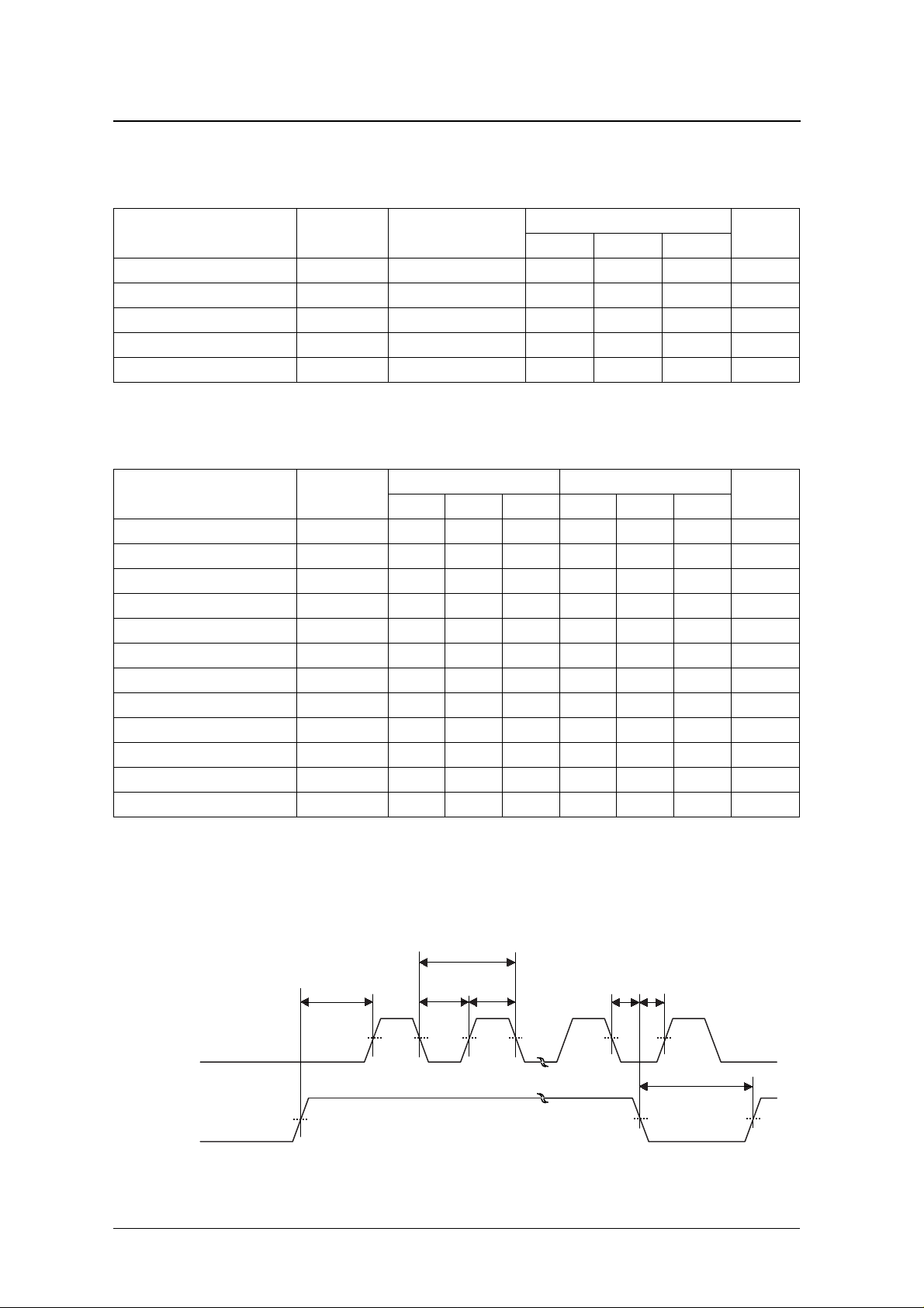
AC Characteristics
V
= 0 V, C
SS
CLK clock period t
CLK HIGH-level pulsewidth t
CLK LOW-level pulsewidth t
CE setup time t
CE hold time t
CE recovery time t
CLK hold time t
Write data setup time t
Write data hold time t
Read data output delay time
Output disable delay time
Input rise and fall time t
1. C
=50pF
L
2. C
=50pF, RL=10k Ω
L
= 50 pF, T
L
= − 40 to 85 ° C unless otherwise noted
a
Parameter Symbol
CLK
WH
WL
CS
CH
CR
CKH
DS
DH
1
2
t
RD
t
RZ
RF
Rating
min typ m ax
V
= 1.6 V – – 5.0 s
DD
Unit
– – 1.5 V
= 1.6 to 5.5 V
DD
V
= 5.0 V
DD
V
= 5.0 V – 15 – pF
DD
V
= 5 V ± 10% V
DD
2 – +2 ppm/V
10 – +10 ppm
= 3.0 V ± 1 0 %
DD
Unit
min typ ma x min typ ma x
600 – – 1200 – – ns
300 – – 600 – – ns
300 – – 600 – – ns
150 – – 300 – – ns
200 – – 400 – – ns
300 – – 600 – – ns
50 – – 100 – – ns
50 – – 100 – – ns
50 – – 100 – – ns
– – 200 – – 400 ns
– – 100 – – 200 ns
––20––40ns
CLK
C E
50%
t
CS
50%
t
WL
t
CLK
t
WH
t
CHtCKH
t
CR
NIPPON PRECISION CIRCUITS—4
 Loading...