NPC SM8224BM, SM8224BS Datasheet

SM8224B
NIPPON PRECISION CIRCUITS INC.
Dual-Tone Receiver IC
OVERVIEW
The SM8224B is a receiver and decoder that supports the Bellcore TR-NWT-000030 and SR-TSV-002476
standards calling number identification (caller ID) and call waiting dual-tone signals. It has separate caller ID
signal and call waiting signal inputs, which allows the gain for each input to be adjusted independently. It is
fabricated in CMOS and features a power-down function, realizing low power dissipation operation.
FEATURES
■
TR-NWT-000030 and SR-TSV-002476 standards
(Bellcore)
■
Call waiting
■
FSK decoder
■
High input sensitivity
■
Independent input gain adjustment for caller ID
signal and call waiting signal inputs
■
Power-down mode
■
Crystal oscillator circuit built-in
■
Single supply operation:4.5 to 5.5V
■
Molybdenum-gate CMOS process
APPLICATIONS
■
Telephones, fax machines and modems that support pre- and mid-conversation information services
■
Adapters for pre- and mid-conversation information service functions
■
Telephone answering machines
■
Facsimile machines
■
Computer peripheral equipment
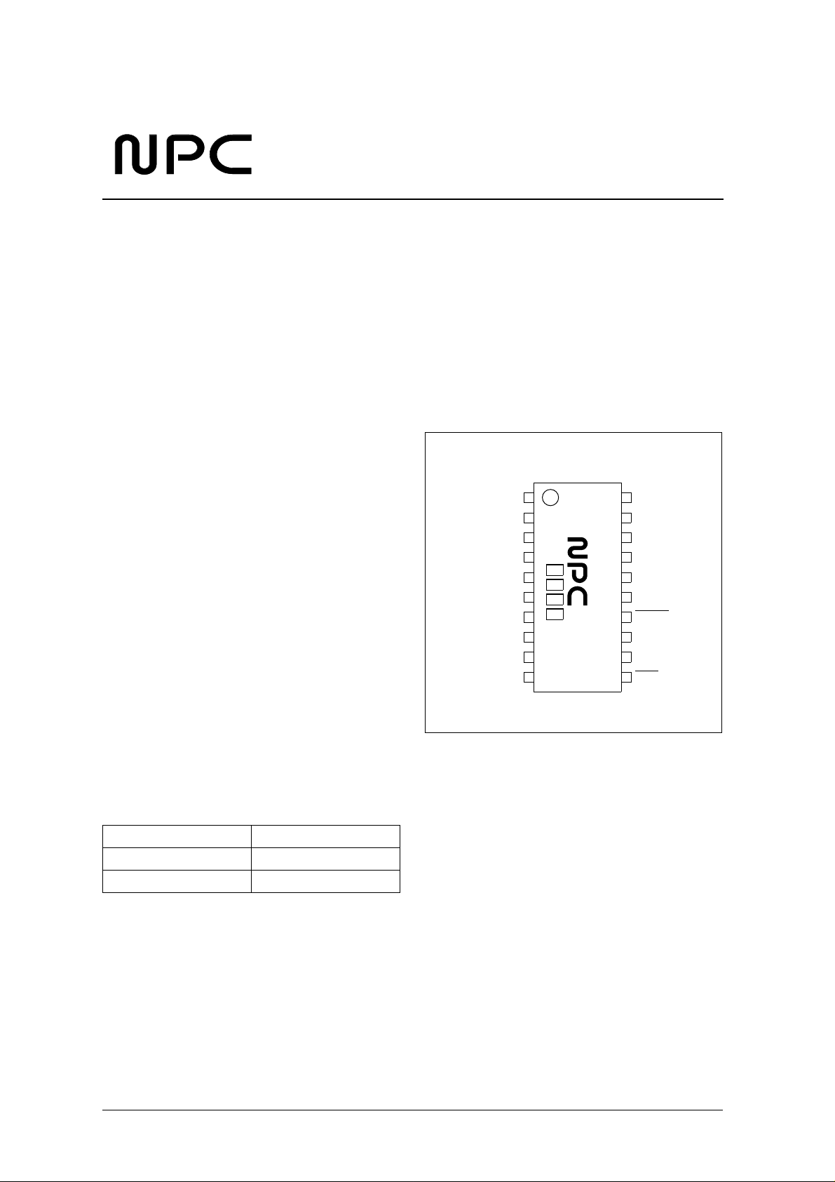
PINOUT
(Top view)
OSCOUT
AGND
TIP
RING
TRQ
GND
OSCIN
MODE
TEST
DOUT
1
20
DT1
DT2
SM8224B
DTQ
S0
S1
VDD
CDET
CR
DTDET
10
11
STR
ORDERING INFORMATION
De vice Pack ag e
SM8224BM 20-pin SSOP
SM8224BS 20-pin SOP
NIPPON PRECISION CIRCUITS—1

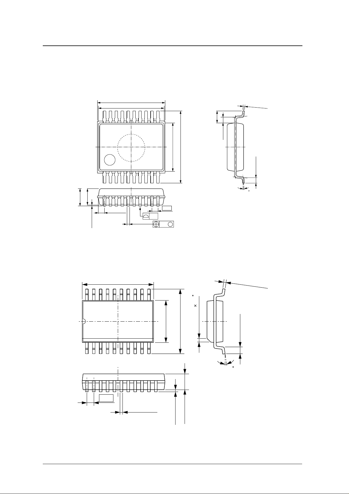
PACKAGE DIMENSIONS
(Unit: mm)
20-pin SSOP
SM8224B
20-pin SOP
2.10 max
1.80 ± 0.10
0.10 ± 0.10
0.68 ± 0.12
7.40 max
7.20 ± 0.05
0.30 ± 0.10
0.10
0.13
0.65
M
5.30 ± 0.05
7.90 ± 0.20
1.30 ± 0.10
0.62 typ
0 to 8
0.20
±
0.6 ± 0.15
0.05
12.75 ± 0.10
1.27
0.41 ± 0.05
7.50 ± 0.10
10.31 ± 0.20
2.34 ± 0.10
0.20 ± 0.10
0.275 ± 0.045
0.51 ± 0.2 45
0.76 ± 0.25
0 to 8
NIPPON PRECISION CIRCUITS—2

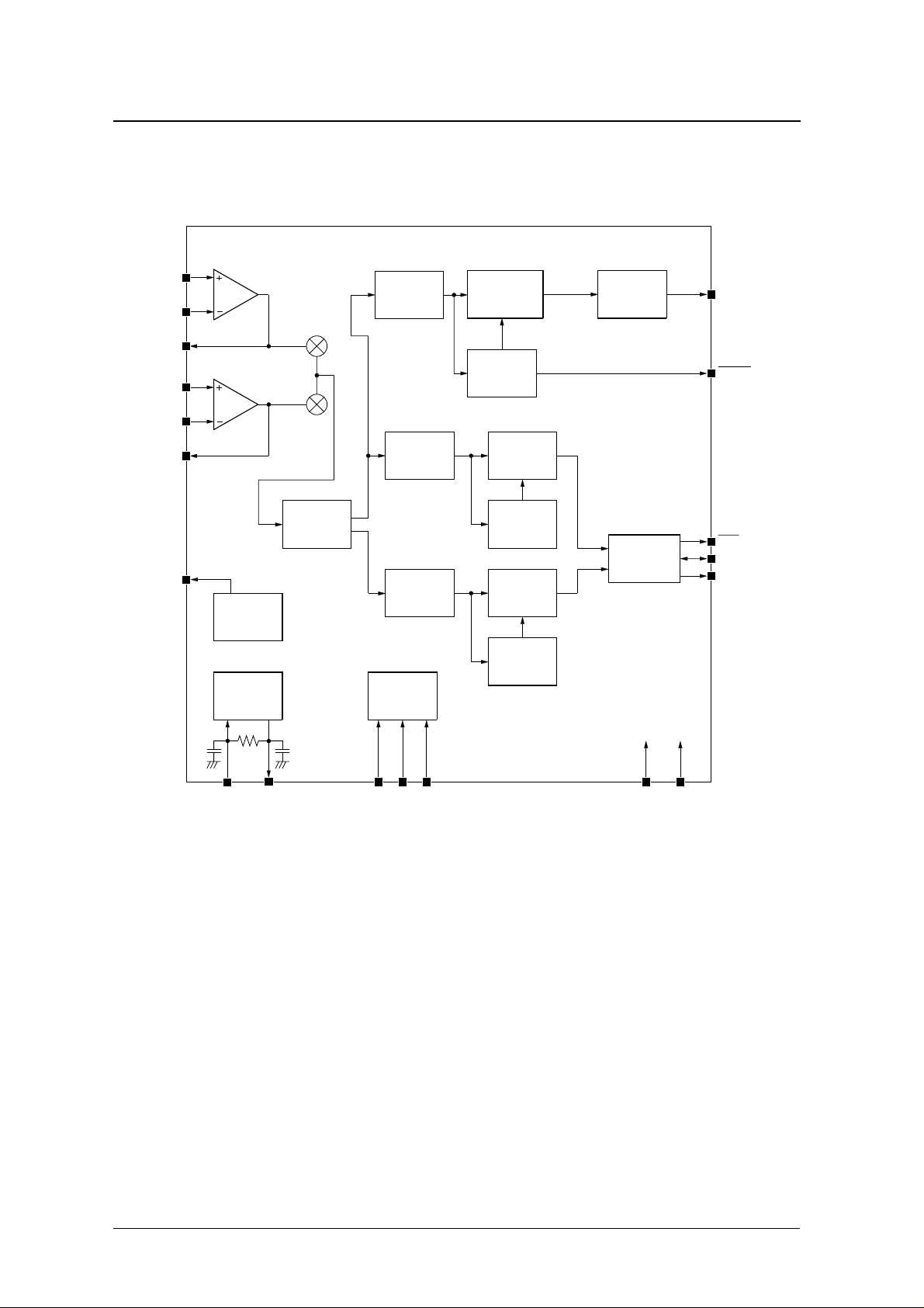
BLOCK DIAGRAM
SM8224B
TIP
RING
TRQ
DT1
DT2
DTQ
AGND
Bias
Circuit
Crystal
Oscillator
Circuit
Filter
Filter
Filter
(2130Hz)
Filter
(2750Hz)
Power-down
Circuit
FSK
Demodulator
Carrier
Detector
Detector
Circuit
(2130Hz)
Level
Detector
Detector
Circuit
(2750Hz)
Level
Detector
Output
Circuit
Time-constant
Circuit
DOUT
CDET
STR
CR
DTDET
OSCIN OSCOUT MODE GNDVDD
S0
S1
NIPPON PRECISION CIRCUITS—3

SM8224B
PIN DESCRIPTION
Number Name I/O Function
1 AG N D O Analog ground output. Internal reference voltage (V
2 TIP I Tip input. Connected to the telephone line through a protection circuit
3 RING I Ring input. Connected to the telephone line through a protection circuit
4 T R Q O Input-stage amplifier gain-select output. Used to adjust the gain of the input-stage amplifier.
5 G ND – Ground. Connected to the system ground potential.
6 OSCIN I Crystal oscillator input. The cr ystal oscillator element is connected between this pin and OSCOUT.
7 OSCOUT O Crystal oscillator output. The crystal oscillator element is connected between this pin and OSCIN.
8 MODE I When MODE is HIGH, and S1 and S0 are both LOW, the device is in power-down state. See table 2.
9 TEST – TEST pin. Set OPEN when normal using.
10 DOUT O Data output. Demodulated FSK signal output. HIGH level output when CDET goes HIGH.
11 STR O
12 DTDET O Dual-tone detector output. HIGH-level output when dual tone is detected.
13 C R I/O
14 CDET O FSK signal carrier detector output. L OW -level when active carrier is detected.
15 VD D – Supply
16 S1 I Function select bit 1. Selects the device mode in combination with S0 and MODE. See table 2.
17 S0 I Function select bit 1. Selects the device mode in combination with S1 and MODE. See table 2.
18 D TQ O Dual-tone signal input-stage amplifier output. Used to adjust the gain of the input-stage amplifier.
19 DT 2 I Dual-tone signal input-stage operational amplifier inverting input
20 DT 1 I Dual-tone signal input-stage operational amplifier non-inverting input
Dual-tone confirmation output. Function is selected by S0 and S1. See table 2.
Dual-tone confirmation: Active-LOW output when dual tone detection signal passes through RC time
constant delay circuit.
Dual tone RC time constant circuit connection. The dual tone detection signal passes through the RC
network to generate the ST R signal.
/2) output level
DD
NIPPON PRECISION CIRCUITS—4
 Loading...