NPC SM8220P, SM8220S, SM8221P, SM8221S Datasheet

NIPPON PRECISION CIRCUITS INC.
NIPPON PRECISION CIRCUITS-1
OVERVIEW
SM8220/SM8221
Calling Number Identification Receiver IC
The SM8220/SM8221 Calling Number Identification
Receiver IC is a CMOS integrated circuit, which provides
an interface to various calling information delivery services
such as Calling Number Delivery (CND) and Calling
Name Delivery (CNAM) compatible with the Bellcore
GR-30-CORE. The device also contains a power down circuit, a ring detect circuit and a carrier detect circuit for easier system implementation.
FEATURES
•Compatible with Bellcore GR-30-CORE
•Integrated band pass filter
•FSK demodulator
Bell 202 and ITU-T V.23
•High input sensitivity: −48 dBm typical
•Ring detect output
•Carrier Detect Output (SM8220)
•Power down mode: 1µA power down current
•Uses 3.579545 MHz crystal (SM8220) or external
clock source
•Power supply voltage: 3V to 5.5V
•Low power consumption
•Molybdenum-gate CMOS process
•Package
SM8220: 16 pin SOP, 16 pin DIP
SM8221: 8 pin SOP, 8 pin DIP
APPLICATIONS
•Calling Number Delivery service
•Adjunct Boxes
•Telephone Answering Machines
•Feature Phones
•Fax Machines
•Computer Interface Products
PINOUT
(Top View)
8
220
1
9
16
8
TIP
RING
AGND
RDIN
RDRC
RDET
PDWN
VDD
FOUT
DMIN
DOUT
NC
CDET
OSCOUT
GND
OSCIN
/CLKIN
1
9
16
8
SM8220S (16pin SOP) SM8220P (16pin DIP)
S
M
8
220
S
MS
P
1
4
5
8
TIP
RING
PDWN
GND
VDD
DOUT
CDET
CLKIN
1
4
5
8
SM8221S (8pin SOP) SM8221P (8pin DIP)
8
221
S
M
P
TIP
RING
AGND
RDIN
RDRC
RDET
PDWN
VDD
FOUT
DMIN
DOUT
NC
CDET
OSCOUT
GND
OSCIN
/CLKIN
TIP
RING
PDWN
GND
VDD
DOUT
CDET
CLKIN
8
221

NIPPON PRECISION CIRCUITS-2
SM8220/SM8221
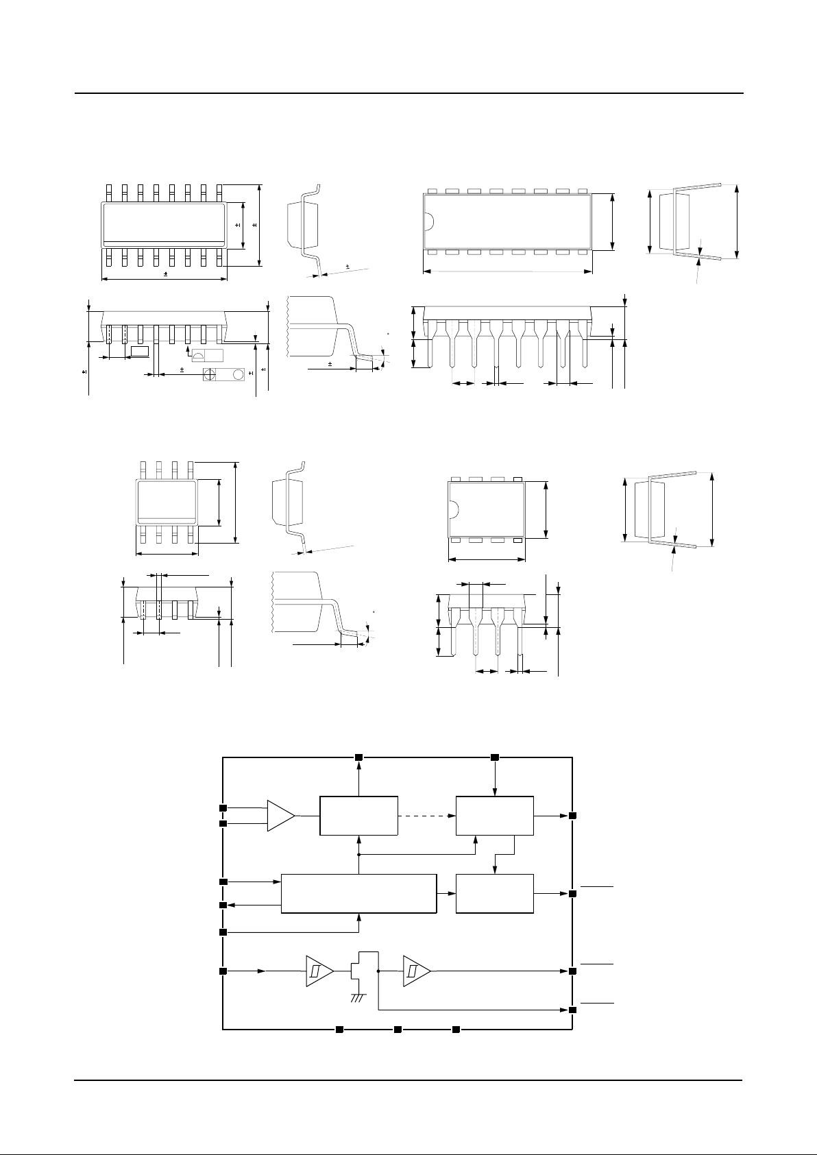
PACKAGE DIMENSIONS
(Unit: mm)
TIP
RING
OSCIN*
/CLKIN
OSCOUT*
PDWN
RDIN*
FOUT* DMIN*
DOUT
CDET
RDET*
Band Pass
Filter
FSK
Demodulator
Power Down Control
and Clock Generator
Carrier
Detect
(SM8221)
AGND* VDD
GND
*: Not available for SM8221.
RDRC*
BLOCK DIAGRAM
19.05
2.54
0.25
2.54 0.46 1.52
3.68 to 4.32
0.38 to 1.02
6.35
3.18 3.30
7.49 to 8.13
8.13 to 9.40
0 to 8
9.89 0.09
6.00 0.20
3.90 0.09
1.375 0.275
1.27
0.25
0.41 0.05
0.10
1.55 0.20
0.175 0.075
M
0.13 0.06
0.84 0.43
SM8220S (16 pin SOP) SM8220P (16 pin DIP)
SM8221S (8 pin SOP) SM8221P (8 pin DIP)
8.89
2.54
0.25
2.54 0.46
1.52
3.68 to 4.32
0.38 to 1.02
6.35
3.18 3.30
7.49 to 8.13
8.13 to 9.40
1.27
0.10 to 0.25
4.80 to 4.98
3.81 to 3.99
0.36 to 0.46
0.19 to 0.25
1.35 to 1.75
1.10 to 1.65
0.41 to 1.27
0 to 8
5.80 to 6.20

NIPPON PRECISION CIRCUITS-3
SM8220/SM8221
PIN DESCRIPTIONS
Number Name i/o Function
SM8220 SM8221
1 1 TIP i
2 2 RING i
3 - AGND o
4 - RDIN si
5 - RDRC od
6 - RDET o
7 3 PDWN si
8 4 GND 9 5 OSCIN i
/CLKIN
10 - OSCOUT o
11 6 CDET o
12 - NC 13 7 DOUT o
14 - DMIN i
15 - FOUT o
16 8 VDD -
(Note) si: Schmitt Triger Input, od: Open Drain Output.
Tip Input: This pin is connected to the tip side of the twisted pair telephone wires.
This pin must be DC isolated from the phone line.
Ring Input: This pin is connected to the ring side of the twisted pair telephone wires.
This pin must be DC isolated from the phone line.
Analog Ground: 1/2 V
DD voltage output. This pin must be grounded through 0.1 µF capacitor.
Ring Detect Input: The attenuated ring signal is connected to this pin for the ring detection.
Ring Detect RC Terminal: An RC network will be connected to this pin to set time delays for
the ring signal detection.
Ring Detect Output: This pin is an output of a schmitt trigger buffer which input is connected
to RDRC pin. The low level at this pin indicates that the ring signal is detected.
Power Down Control: This pin must be kept at low level for the normal operation.
When it is high, the device will be in the power down.
Under the power down mode, OSCOUT, CDET and DOUT pins are set to high level and
AGND, FOUT pins are set to high impedance.
Device Ground: This pin is connected to the system ground.
Crystal Oscillator Input: A crystal will be connected between this pin and OSCOUT pin.
This pin may be driven from an external clock source.
Crystal Oscillator Output: A crystal will be connected between this pin and OSCIN pin.
This pin must be kept open when OSCIN pin is driven from an external clock source.
Carrier Detect Output: When low, this output indicates that a valid carrier present on the line.
No connection pin.
Data Out: This pin presents the output of the demodulator while CDET pin is low.
When CDET pin goes high, this pin is held high.
Demodulator Input: This pin is connected from FOUT pin through a 0.1µF capacitor.
No other components should be connected to this pin.
Band Pass Filter Output: This pin is connected to DMIN pin through a 0.1µF capacitor.
No other components should be connected to this pin.
Power Supply: Positive power supply pin.
 Loading...