NPC SM8213AM Datasheet
SM8213AM
NIPPON PRECISION CIRCUITS INC.
POCSAG Decoder For Multiframe Pagers
OVERVIEW
The SM8213AM is a POCSAG-standard (Post
Office Code Standardization Advisory Group) signal
processor LSI, which conforms to CCIR recommendation 584 concerning standard international wireless calling codes.
The SM8213AM supports call messages in either
tone, numerical or character outputs at signal speeds
of 512, 1200 or 2400 bps. The signal input stage features a built-in filter.
Each of the addresses (max. 7 + 1 dummy = 8) can
be assigned to any frame, which also makes the
device configurable for many additional services.
Each address can be independently set to ON/OFF.
Furthermore, built-in buffer memory means decoded
information can be fetched in sync with the microcontroller clock, thereby reducing the microcontroller CPU time required. Intermittent-duty method
(battery saving (BS) method) control signals, compatible with PLL operation, and Molybdenum-gate
CMOS structure makes possible the construction of
low-voltage operation, low power dissipation systems.
25 to 75% duty factor signal coverage
■
8 rate error detection condition settings
■
76.8 kHz system clock (crystal oscillator)
■
76.8 or 38.4 kHz clock output pin
■
Built-in oscillator capacitor and feedback resistor
■
2.0 to 3.5 V operating supply voltage
■
Molybdenum-gate CMOS process realizes low
■
power dissipation
16-pin SSOP
■
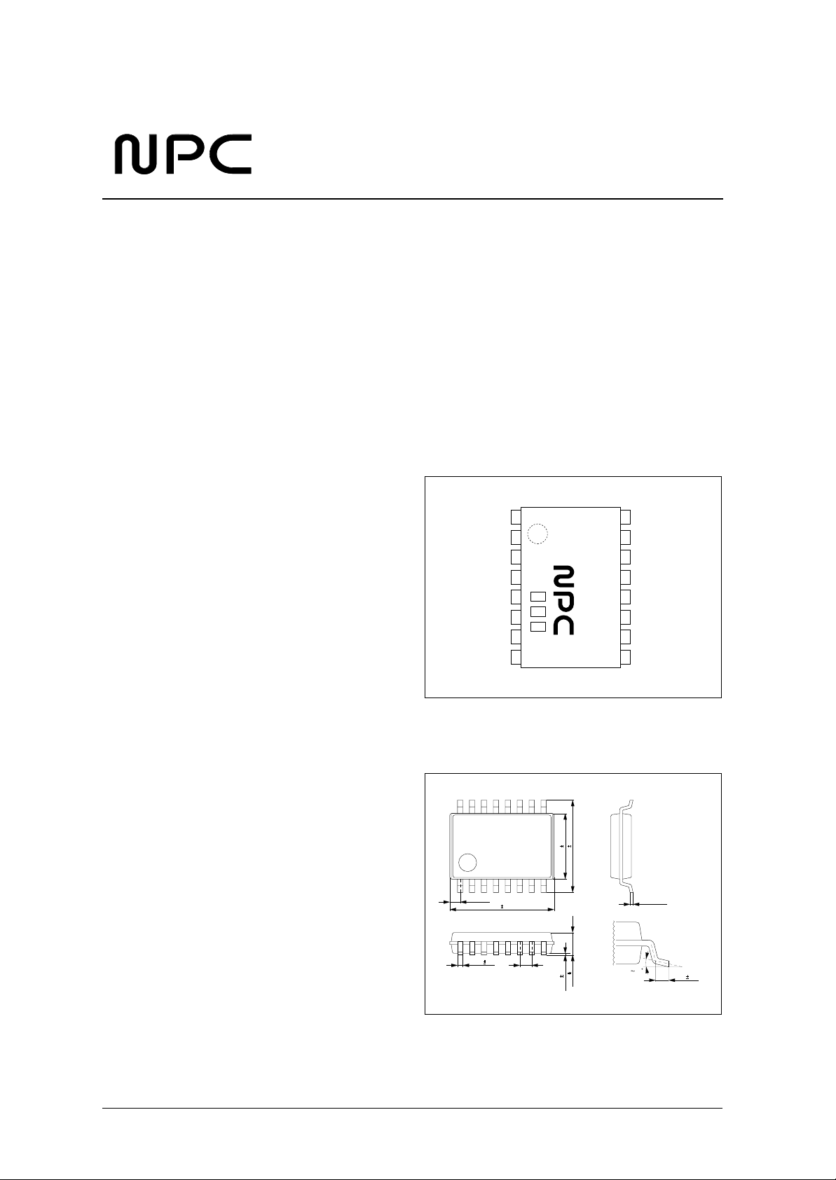
PINOUT
T op V iew
BS1
BS2
BS3
SIGNAL
XT
XTN
1
8
16
8213AM
VDD
ATTN
SDI
SDO
SCKXVSS
AREA
RSTN
9
CLKOVSS
The SM8213AM is available in 16-pin SSOPs.
FEATURES
Conforms to POCSAG standard for pagers
■
512, 1200 or 2400 bps signal speed
■
Multiframe compatible (each address individually
■
controllable)
8 addresses × 4 sub-addresses (total of 32
■
addresses) control
(8 addresses comprise 7 actual addresses + 1
dummy address)
Built-in buffer memory (1 code word)
■
Supports tone, numeric or character call messages
■
Built-in input signal filter, with filter ON/OFF and
■
4 selectable filter characteristics
PLL-compatible battery saving method (BS1,
■
BS2, BS3 outputs)
BS1 (RF control main output signal) 61-step setup
■
time setting
BS3 (PLL setup signal) 61-step setup time setting
■
BS2 (RF DC-level adjustment signal) before/dur-
■
ing reception selectable adjustment timing
1-bit and 2-bit burst error auto-correction function
■
PACKAGE DIMENSIONS
Unit: mm
4.4 0.2
6.2 0.3
0.6TYP
6.8 0.3
0.80.36 0.1
1.5 0.1
0.05 0.05
010
0.15
+ 0.10
- 0.05
0.4 0.2
NIPPON PRECISION CIRCUITS—1
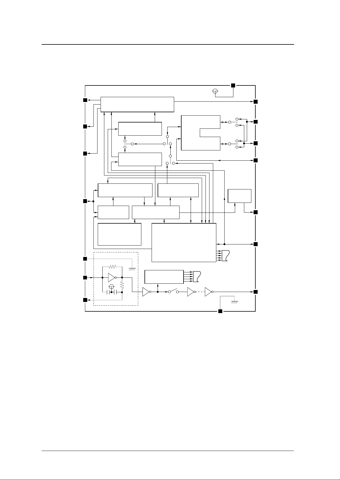
BLOCK DIAGRAM
SM8213AM
VDD
BS1
BS2
BS3
SIGNAL
XVSS
Timing Control
Flag Register
Address Register
Receive Data Register
Digital PLL
Preamble Pattern
Sync Code
Idle Code
Data Comparator
Buffer Register
(Ring)
Buffer Register
Error Correction
Main Control
Circuit
ATTN
SDI
SDO
SCK
Timer
AREA
RSTN
Each Switch
and Register
XT
XTN
Clock Control
Each Working Block
CLKO
VSS
NIPPON PRECISION CIRCUITS—2
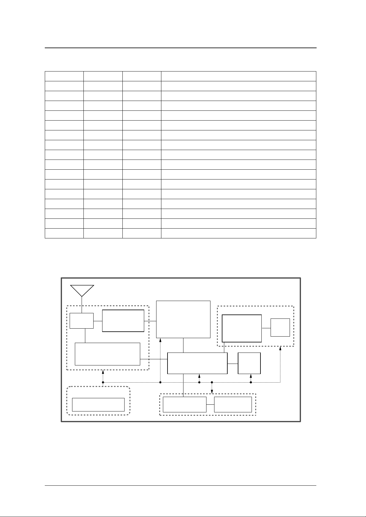
PIN DESCRIPTION
SM8213AM
Number Name I/O
1 BS1 O RF control main output signal
2 BS2 O RF DC-level adjustment signal
3 BS3 O PLL setup signal
4 SIGNAL I NRZ signal input pin
5 XVSS – Crystal oscillator ground. Capacitor connected between XVSS and VDD
6 XT I Oscillator input pin
7 XTN O Oscillator output pin
8 VSS – Ground
9 CLKO O 76.8 or 38.4 kHz clock output
10 RSTN I Hardware clear (reset)
11 AREA O Sync code detection output (HIGH for minimum 1 sec. on detection)
12 SCK I CPU-to-decoder data transfer sync clock
13 SDO O Status and received data output to CPU
14 SDI I Data input from CPU (including ID data)
15 ATTN O Interrupt detect signal output pin (Ready for data transmission when LOW)
16 VDD – Supply voltage
1. I = input, O = output
1
Description
SM8213AM Paging Receiver Block Diagram
POCSAG
RF
Waveform
Recovery
Decoder
SM8213
PLL Circuit
CPU Unit
Supply Unit
D/D Converter LCD Driver
Alert
Melody
SP
IC
ID
ROM
LCD
NIPPON PRECISION CIRCUITS—3
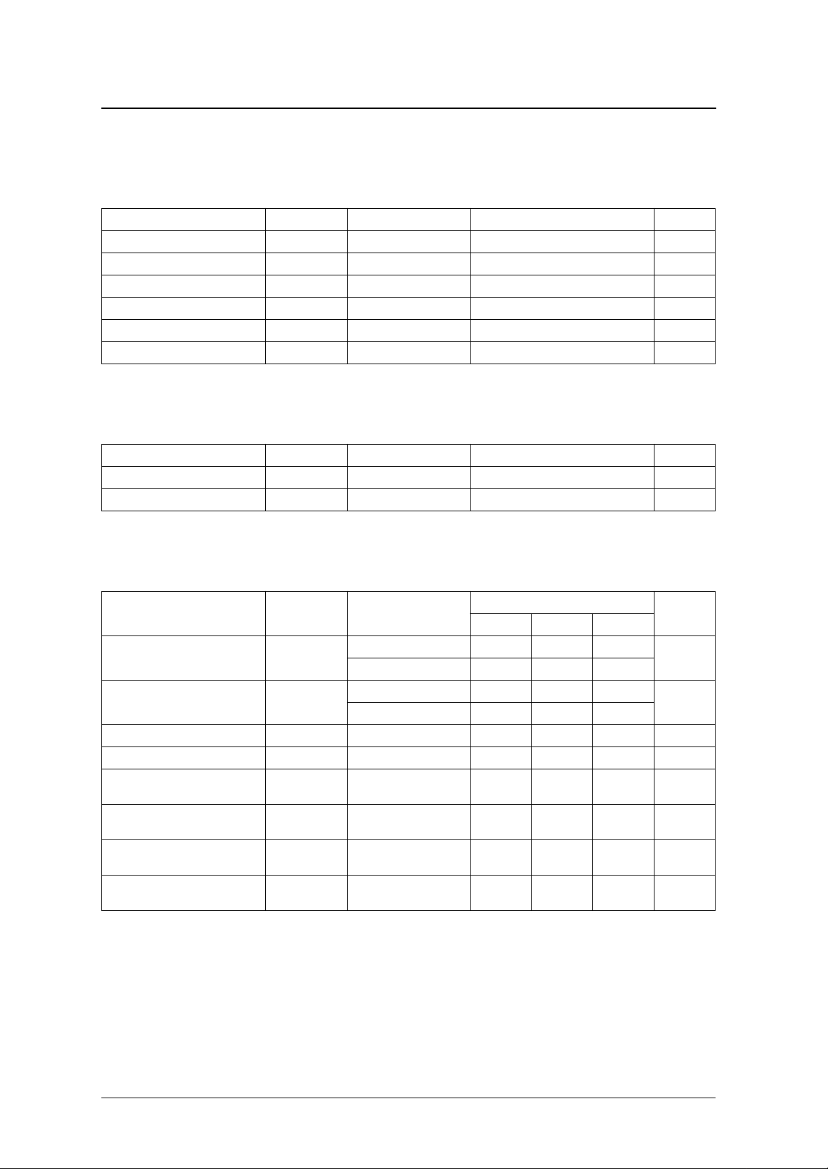
SPECIFICATIONS
Absolute Maximum Ratings
V
= 0 V
SS
Parameter Symbol Condition Rating Unit
Supply voltage range V
Input voltage range V
Power dissipation P
Storage temperature range T
Soldering temperature T
Soldering time t
Recommended Operating Conditions
DD
IN
D
stg
sld
sld
SM8213AM
−
0.3 to 7.0 V
−
V
0.3 to V
SS
+ 0.3 V
DD
250 mW
−
40 to 125
255
° C
° C
10 s
V
= 0 V
SS
Parameter Symbol Condition Rating Unit
Supply voltage range V
Operating temperature range T
DD
opr
DC Characteristics
Recommended operating conditions unless otherwise noted
Parameter Symbol Condition
V
= 3.0 V – 3.0 6.0
Operating current consumption
(IDLE mode)
Standby supply current
1
2
HIGH-level input voltage (all inputs) V
LOW-level input voltage (all inputs) V
HIGH-level output current
(all outputs except XTN)
LOW-level output current
(all outputs except XTN)
HIGH-level output current
(all outputs except XTN)
LOW-level output current
(all outputs except XTN)
I
I
DD1
DD2
I
OH
I
OL
I
OH
I
OL
IH
IL
DD
V
= 2.0 V – 2.0 4.0
DD
V
= 3.0 V – 3.0 6.0
DD
V
= 2.0 V – 2.0 4.0
DD
V
OH
V
OL
V
OH
V
OL
= 2.6 V, V
= 0.4 V, V
= 1.6 V, V
= 0.4 V, V
= 3.0 V 0.6 1.4 – mA
DD
= 3.0 V 1.0 2.2 – mA
DD
= 2.0 V 0.3 0.7 – mA
DD
= 2.0 V 0.7 1.5 – mA
DD
2.0 to 3.5 V
−
20 to 70
Rating
min typ max
0.8V
DD
––V
– – 0.2V
° C
Unit
µA
µA
DD
V
1. CLKO output is inactive. The consumption current is slightly higher when RSTN is going LOW.
2. Oscillator circuit is working.
NIPPON PRECISION CIRCUITS—4
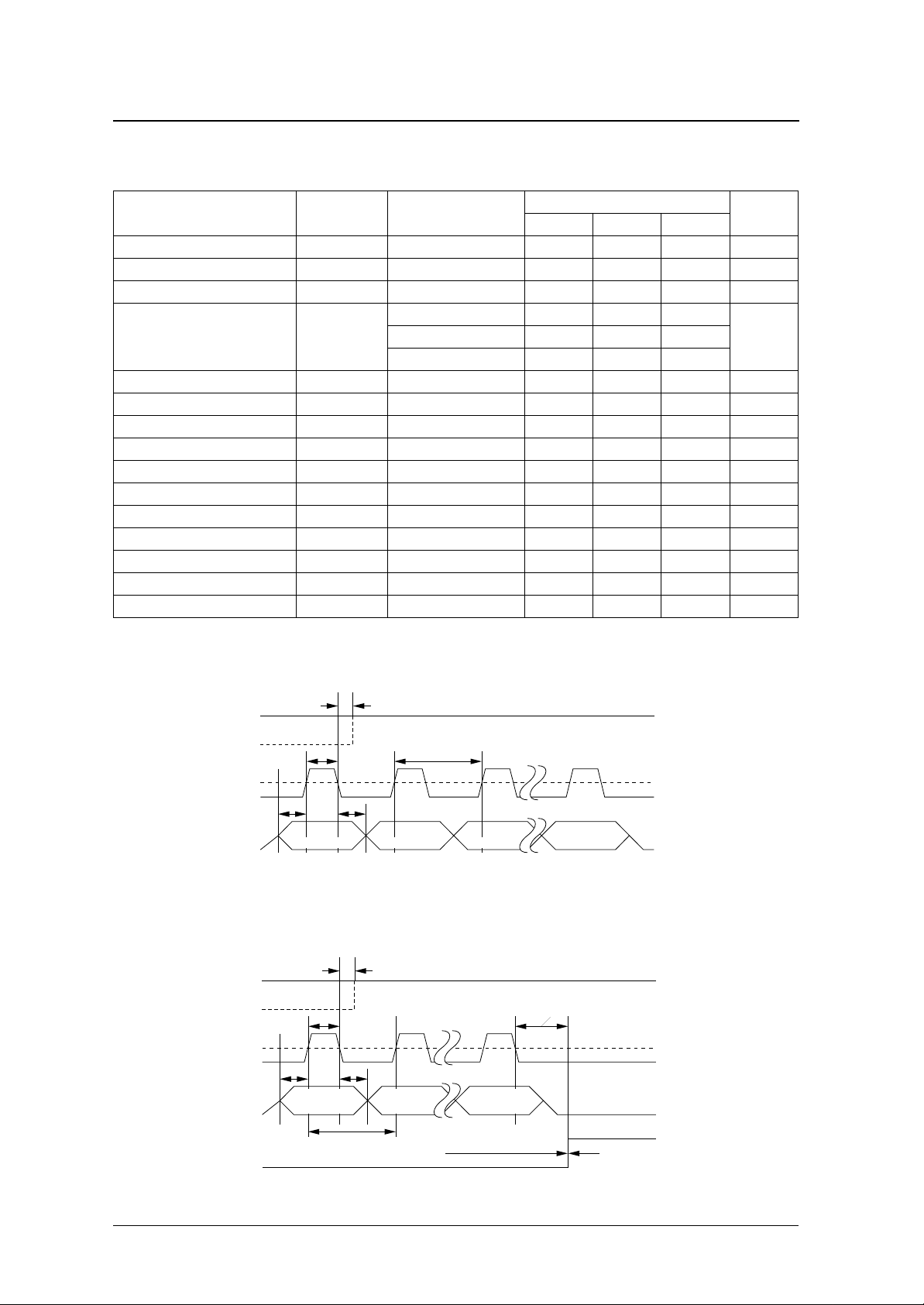
SM8213AM
AC Characteristics
Recommended operating conditions unless otherwise noted
Parameter Symbol Condition
XT clock frequency f
XT clock duty cycle D
SCK clock pulsewidth t
SCK clock interval
(except WRITE mode)
SCK clock interval (WRITE mode) t
SDI data setup time t
SDI data hold time t
SDO data setup time t
SDO data hold time t
ATTN data setup time t
ATTN data hold time t
CLKO clock rise time t
CLKO clock fall time t
CLKO clock delay time D
RSTN pulsewidth t
CYXT
XT
PWSC
t
CYSC
CYSC
SSDI
HSDI
SSDO
HSDO
SATT
HATT
RCLK
FCLK
CLKO
PWRS
512 bps 5 – 1900
2400 bps 5 – 415
No load – – 500 ns
No load – – 500 ns
Rating
min typ max
−
250 ppm 76.8 +250 ppm kHz
Unit
25–75%
2 – 150 µs
µs1200 bps 5 – 830
5 – 830 µs
1––µs
1––µs
3––µs
––0µs
0––µs
1––µs
––1µs
1––ms
Parameter/address set timing
tHATT
ATTN
tPWSC
SCK
12332
tSSDI tHSDI
SDI
INPUT
DATA 1
Auxiliary operating mode set timing
tHATT
ATTN
tPWSC
SCK
SDI
128
Decoder
Setting1
tCYSC
1/ 2*VDD
INPUT
DATA 2
INPUT
DATA 3
START command : 66 bit time max
Others : 2 bit time max
INPUT
DATA 32
1/ 2*VDD
tHSDItSSDI
Decoder
Setting 2
Decoder
Setting 8
Decoder Mode
tCYSC
Next ModeCurrent Mode
NIPPON PRECISION CIRCUITS—5
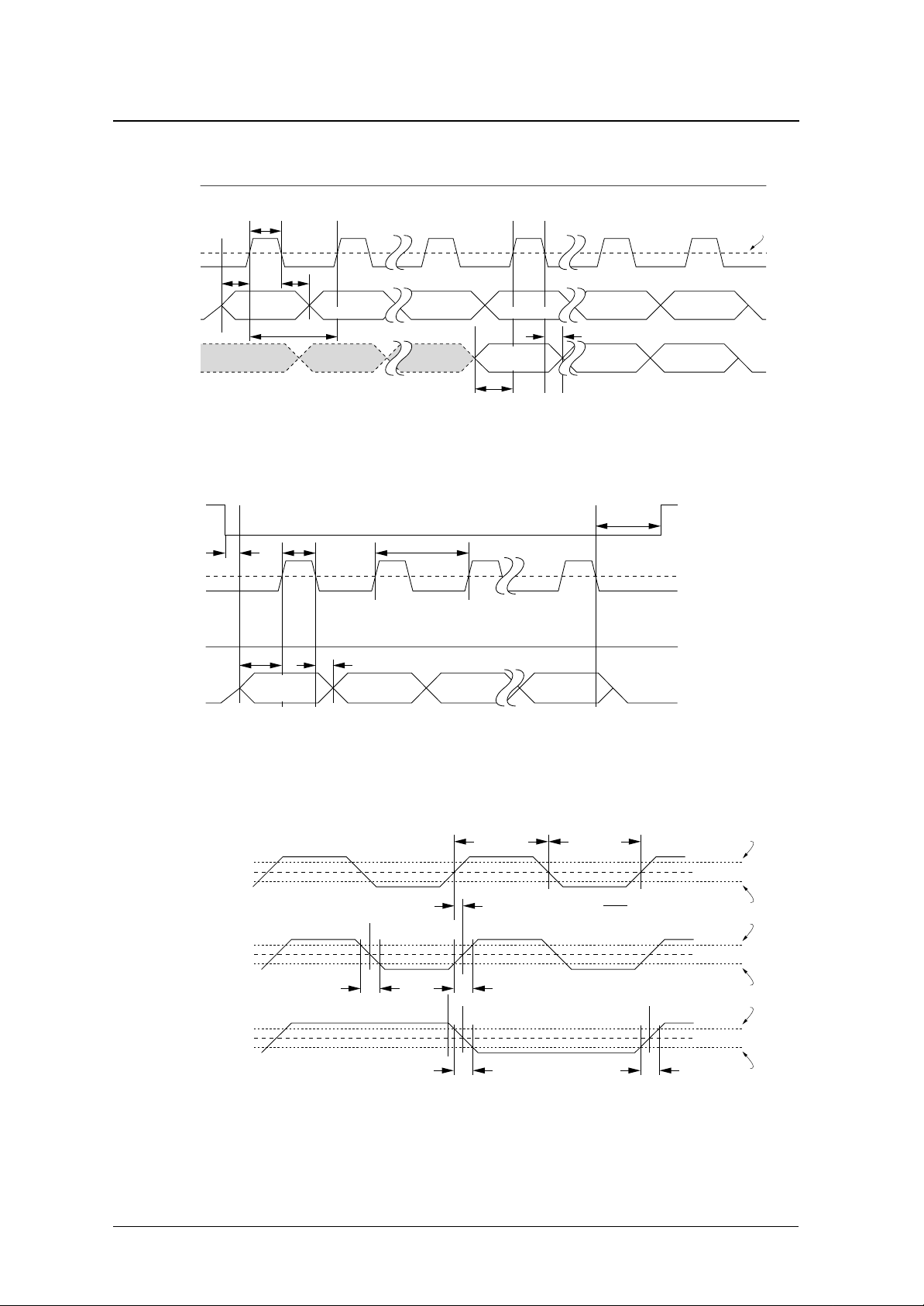
Status data read timing
ATTN
tPWSC
SCK
1289
tHSDItSSDI
SDI
READ
COMMAND 1
tCYSC
SDO
Don't
Care 1
Received data transfer timing
READ
COMMAND 2
Don't
Care 2
SM8213AM
READ
COMMAND 8
Don't
Care 8
COMMAND 9
STATUS
DATA 1
tSSDO
READ
tHSDO
15 16
READ
COMMAND 15
STATUS
DATA 7
READ
COMMAND 16
STATUS
DATA 8
1/ 2*VDD
ATTN
tSATT
SCK
SDI
tSSDO tHSDO
SDO
CLKO clock output timing
(XT)
(76.8kHz)
CLKO
(76.8kHz Mode)
OUTPUT
DATA 1
tHATT
tPWSC
12332
OUTPUT
DATA 2
tCYSC
DCLKO
OUTPUT
DATA 3
OUTPUT
DATA 32
αβ
α
XT =
D
α+β
tRCLKtFCLK
1/ 2*VDD
0.7*VDD
1/ 2*VDD
0.3*VDD
0.7*VDD
1/ 2*VDD
0.3*VDD
0.7*VDD
CLKO
(38.4kHz Mode)
1/ 2*VDD
tRCLKtFCLK
NIPPON PRECISION CIRCUITS—6
0.3*VDD
FUNCTIONAL DESCRIPTION
SM8213AM
Unless otherwise specified, values in diagrams without parentheses are for 512 bps, in ( ) are for 1200
value of PL5 (MSB) to PL0 (LSB), and “N” represents the value of RF5 (MSB) to RF0 (LSB).
bps, and in [ ] are for 2400 bps. “M” represents the
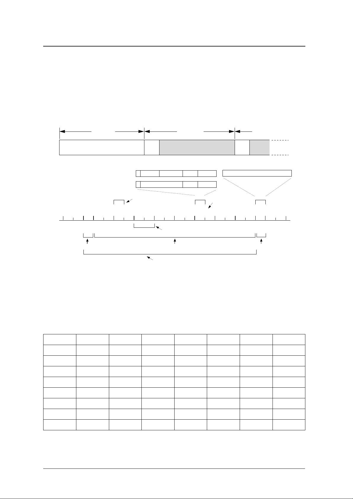
Receive Format
The receive format conforms to CCIR RPC No. 1 (POCSAG).
Preamble 1st Batch 2nd Batch
Continuous 575 - bit "1, 0" bit pattern
Address signal
Message signal
7
SC
01
Sync
Code
12
0
1
19 20 21 22 31
Address bits Function bits Check bits
Message bits
1 Code Word
234
1 Frame(= 2 Code Words)
Check bits
Sync
Code
32
Even - parity bit
Even - parity bit
1
Sync Code Word
Frame No.
567
SC
32
0
Sync Code Part
Frame Part
Sync Code Part
1 Batch
Figure 1. Receive signal format
Sync signal (SC)
The sync signal is a continuous code word in the
received signal, used for word synchronization. It
even-parity bit, making a 32-bit signal. The sync
code word pattern is shown in table 1.
comprises 31 bits in an M-series bit pattern plus one
Table 1. Sync code format
Bit number Bit value Bit number Bit value Bit number Bit value Bit number Bit value
1091170251
2 1101180261
3 1110190270
4 1121201281
5 1130210291
6 1140221300
7 0151230310
8 0160241320
NIPPON PRECISION CIRCUITS—7
SM8213AM
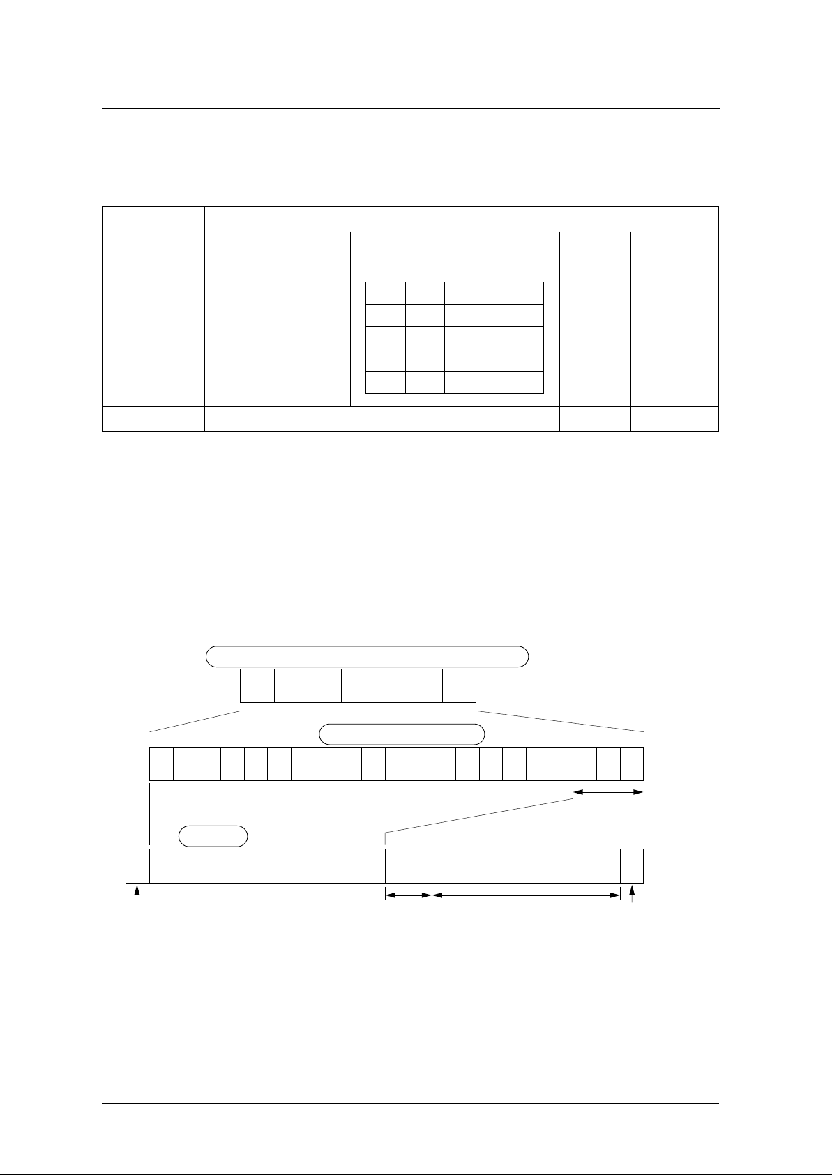
Code words (address and message signals)
Each code word comprises 32 bits as shown in table 2.
Table 2. Code word format
Code word
Address signal 0 Address bits
Message signal 1 Message bits Check bits Even-parity bit
1. The MSB is the address/message code word control bit. It is 0 for an address signal, and 1 for a message signal.
2. Bits 2 to 21 contain the address or message information.
3. Bits 22 to 31 are BCH(31,21) format generated check bits, where BCH(n,k) = BCH(word length, number of information bits).
4. The LSB is an even-parity bit for bits 1 to 31.
1 (MSB)
1
2 to 19
2
Function bits
20 21 Function
0 0 A call
0 1 B call
1 0 C call
1 1 D call
Bit number
2
20, 21
3
22 to 31
Check bits Even-parity bit
32 (LSB)
Call number to call sign conversion
This conversion expands a 7-digit decimal call number into a 21-bit binary call sign, as shown in figure
2.
After expansion, the high-order 18 bits are assigned
to bits 2 to 19 (address signal), and the low-order 3
bits are the user-defined frame identification pattern,
which is stored in ID-ROM. The two function bits
define which of four call functions is active.
4
7 - digit decimal call signal (gap code) (8 to 2000000)
1234567
MSB LSB
21 - bit binary conversion
123456789101112131415161718192021
identification
1 2 19 20 21 323122
0
Flag : "0" = Adderss signal
Call sign
Bits 2 to 19 (18 bits)
Function bits
Bits 22 to 31 (10 bits)
BCH(31, 21) generated check bits
Figure 2. Call number to call sign conversion
Frame
pattern
P
Even - parity bit
(for bits 1 to 31)
NIPPON PRECISION CIRCUITS—8
Idle signal
SM8213AM
In the POCSAG format, for pager systems that send
numeric data, the message information content varies and as a result an idle signal or another address
signal is inserted after the message to indicate the
end of the message.
That is, if no address word or message word exists
for a frame within a batch or for a code word within
a frame, the idle pattern, shown in table 3, is trans-
Table 3. Idle code format
Bit number Bit value Bit number Bit value Bit number Bit value Bit number Bit value
1091171251
2 1100181260
3 1110190270
4 1120200281
5 1131210290
6 0140220301
7 1150230311
8 0161241321
mitted in its place. Then during message signal
reception, the message ends when the idle signal is
detected.
The SM8213AM supports 2 methods of determining
the end of message. Namely, a message ends when
either an idle signal or another address is received
(POCSAG format), or when an interrupt signal from
the CPU is received.
Receive signal duty factor
During preamble detection, the preamble pattern
(1,0) is recognized at duty factors from 25% (min) to
75% (max) of the (1,0) preamble cycle.
Error correction and detection
The SM8213AM performs error correction (or
detection) on each code word as described in table 4.
Table 4. Error correction
Item Description
Preamble Pattern Detection Selectable 1 to 8 rate errors in 6 to 544 bits
Synchronization Code word Detection 2 random errors in 32 bits
Self Address Code word Detection 2 random errors in 32 bits
Message Code word 1-bit and 2-bit burst errors in 31 bits
An error is deemed to have occurred when 2 or more
signal edges occur within 1-bit unit time, and a rate
error is deemed to have occurred when the number of
Note that there are 8 selectable error correction conditions for the preamble pattern.
errors exceeds the counter value. Refer to the “Preamble Mode” section for a discussion of the error
counter.
NIPPON PRECISION CIRCUITS—9
Battery Saving (BS1, BS2, BS3)
SM8213AM
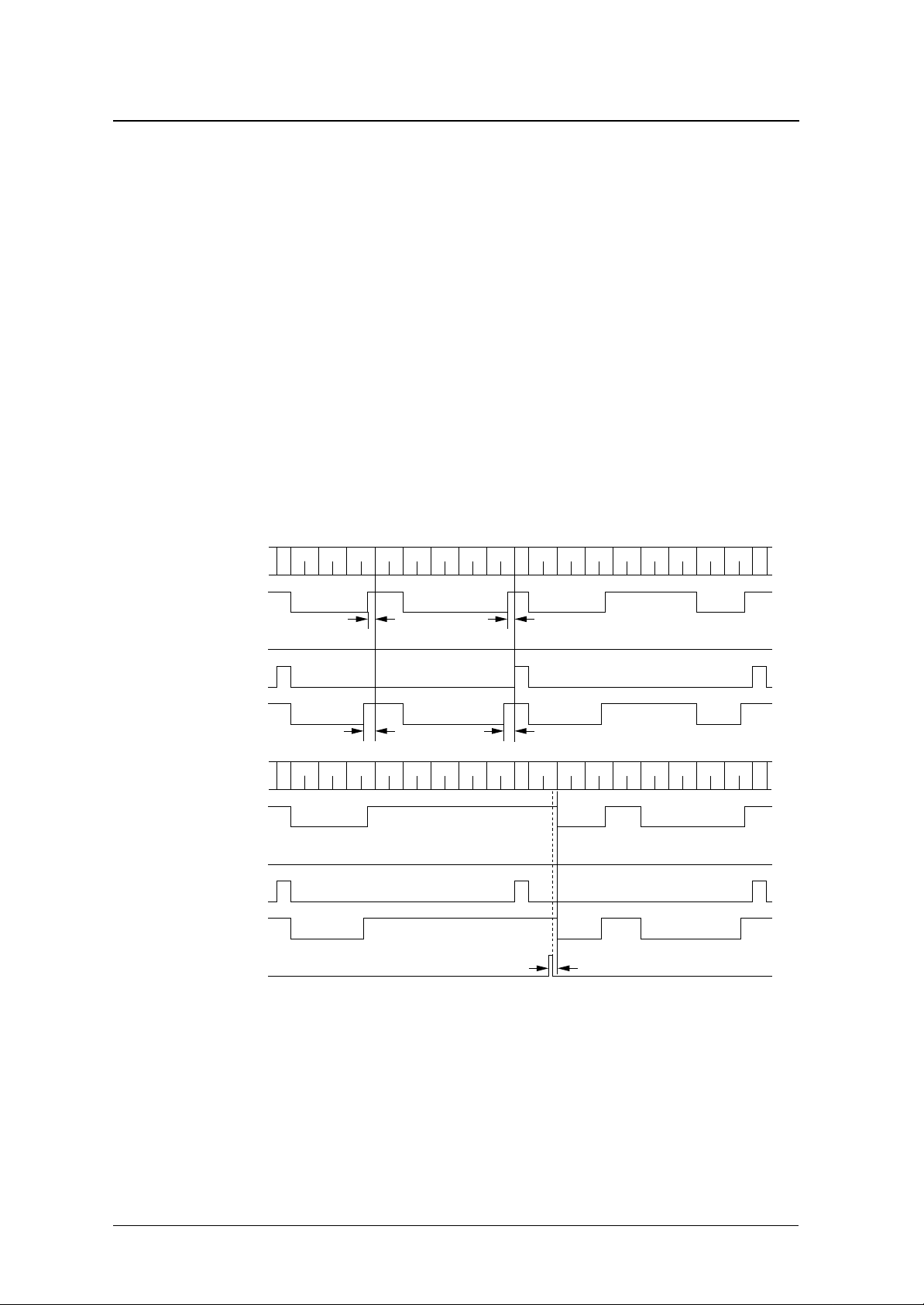
The SM8213AM controls the intermittent-duty operation of the RF stage, which reduces battery consumption, and three output control signals (BS1,
BS2, BS3). The function each signal controls in each
mode is described below.
■
BS1 (RF-control main output signal)—The RF
stage is active when BS1 is HIGH. The risingedge setup time for receive timing is set by flags
RF0 to RF5 (61 steps). The maximum setup time
is 25.417 ms at 2400 bps, 50.833 ms at 1200 bps,
and 119.141 ms at 512 bps. Note that 3E
and
H
3FH are invalid settings for BS1.
■ BS2 (RF DC-level adjustment signal)—BS2 is
used to control the discharge of the receive signal
DC-cut capacitor. The function of BS2 is determined by flag BS2, as described below.
• When flag BS2 is 0, pin BS2 goes HIGH
together with BS1 and then goes LOW again
Receive code
BS1
01234567 01 345672
SYN
ICW
MES
ADD
ICW
MES
ICW
ADD
MES
MES
MES
Address does not match
after the BS1 setup time (idle mode). In preamble and lock mode (during address/message
reception), it stays LOW.
• When flag BS2 is 1, pin BS2 goes HIGH during
lock mode sync code receive timing and idle
mode signal receive timing. In preamble mode,
it stays LOW.
■ BS3 (PLL setup signal)—BS3 is used to control
PLL operation when the PLL is used. The risingedge setup time for receive timing is set by flags
PL0 to PL5 (61 steps). The maximum setup time
is 25.833 ms at 2400 bps, 51.667 ms at 1200 bps,
and 121.094 ms at 512 bps. Note that 3F
invalid setting for BS3.
Note that the setup times should be set up such that
(BS3 rising-edge setup time) > (BS1 rising-edge
setup time).
MES
ICW
ICW
ICW
ADD
MES
SYN
MES
MES
MES
MES
ICW
ICW
ADD
MES
MES
MES
MES
ICW
ADD
Self address
MES
ADD
is an
H
MES
SYN
BS2
(flag BS2 option = 0)
BS2
(flag BS2 option = 1)
BS3
Receive code
BS1
BS2
(flag BS2 option = 0)
BS2
(flag BS2 option = 1)
BS3
BREAK command
1.953*Nms (0.833*Nms)
[0.417*Nms]
1.953*Mms
(0.833*Mms) [0.417*Mms]
01234567 01 345672
SYN
MES
MES
ICW
ICW
ICW
ICW
ADD
Self address
1.953*Mms
(0.833*Mms) [0.417*Mms]
MES
MES
MES
MES
MES
MES
1.953*Nms (0.833*Nms)
[0.417*Nms]
MES
MES
MES
SYN
MES
MES
MES
ICW
ADD
MES
MES
BREAK detection to reception stop (32 bit max.)
Figure 3. BS1, BS2 and BS3 timing (Lock mode, frame 3)
MES
MES
ICW
ADD
MES
MES
ICW
ICW
ICW
SYN
NIPPON PRECISION CIRCUITS—10
 Loading...