SM8211M
NIPPON PRECISION CIRCUITS INC.
OVERVIEW
The SM8211M is a POCSAG-standard (Post Office
Code Standardization Advisory Group) signal processor LSI, which conforms to CCIR recommendation 584 concerning standard international wireless
calling codes.
The SM8211M supports call messages in either tone,
numerical or character outputs at signal speeds of
512 bps or 1200 bps using a 76.8 kHz system clock,
or 2400 bps using a double-speed 153.6 kHz system
clock. Note that output timing values for 2400 bps
mode operation are not shown in this datasheet, but
can be obtained by halving the values for 1200 bps
mode operation.
CMOS structure and low-voltage operation realize
low power dissipation, plus an intermittent-duty
receive method (battery-saving function) reduces
battery consumption.
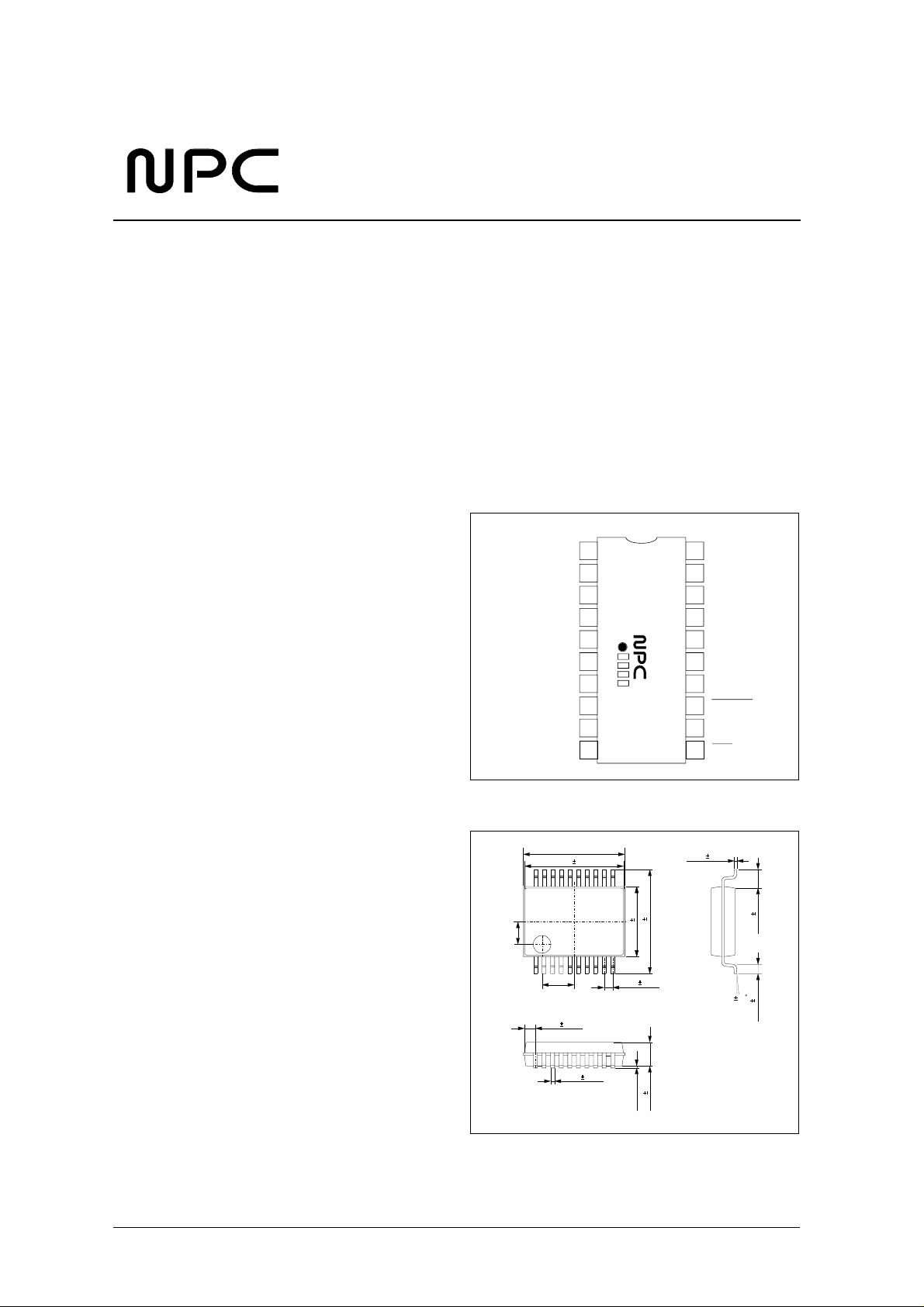
The SM8211M is available in 20-pin SSOPs.
FEATURES
■
Conforms to POCSAG standard for pagers
■
512 or 1200 bps signal speed
■
Supports tone, numeric or character call messages
■
Battery-saving function for low battery consumption
■
BS1 (RF control main output signal) and BS3
(PLL setup signal) 60-step setup time setting—for
BS3, 50.8 ms (max) at 1200 bps and 119.1 ms
(max) at 512 bps
Note that (BS3 setup time) − (BS1 setup time)
should be set to ≥ 2.
■
BS2 (RF DC-level adjustment signal) before/during reception selectable adjustment timing
■
6 addresses × 4 sub-addresses (total of 24
addresses)
■
1-bit and 2-bit burst error auto-correction function
(messages only)
■
25 to 75% duty factor signal coverage (during preamble detection)
■
8 rate error detection condition settings
■
8 receive mode settings
■
76.8 or 153.6 kHz system clock (crystal oscillator
or external clock input)
■
Built-in oscillator capacitor
POCSAG Decoder For Pagers
Built-in input signal filter, with filter ON/OFF and
■
4 selectable filter characteristics
1.2 to 3.5 V (76.8 kHz system clock) or 2.0 to 3.5
■
V (153.6 kHz system clock) operating supply voltage
Molybdenum-gate CMOS process realizes low
■
power dissipation
20-pin SSOP
■
PINOUT
1XVDD
2BS1
3BS2
4BS3
5VDD
6TEST1
7TEST2
8TX-CLK
9TX-DATA
10BREAK 11 RST
PACKAGE DIMENSIONS
7.40max
7.20 0.05
1.50
2.35
0.68 0.12
0.30 0.15
5.30 0.05
0.65 0.12
− 0.10
+ 0.05
0.15
SM8211M
7.90 0.20
1.80 0.05
20 XTN
19 XT
18 SYN-VAL
17 RX-CLK
16 ADD-DET
15 VSS
14 SIG-IN
13 BACKUP
12 RX-DATA
0.20 0.05
4
4
1.30 0.10
0.60 0.15
NIPPON PRECISION CIRCUITS—1
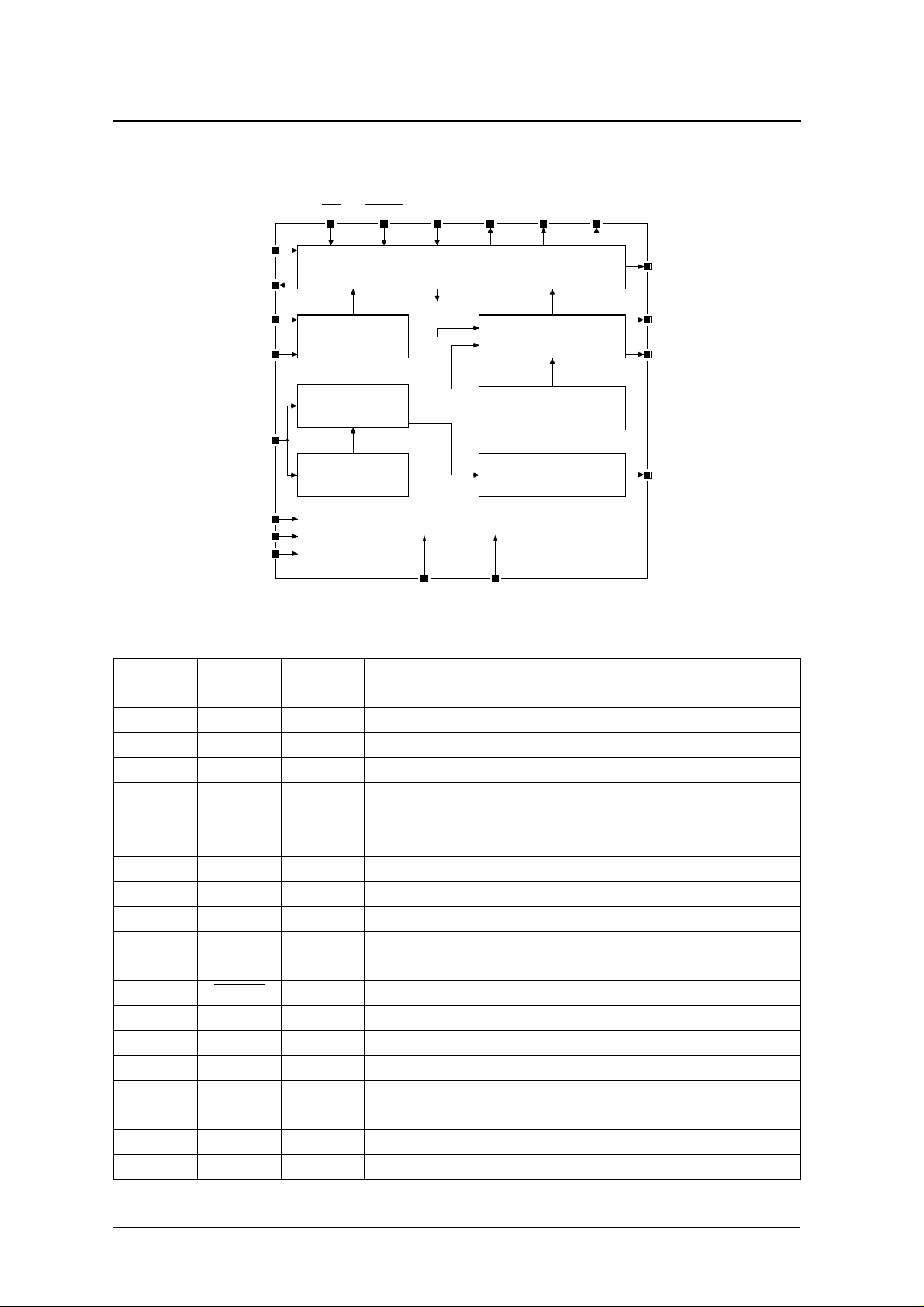
BLOCK DIAGRAM
SM8211M
XT
XTN
TX-CLK
TX-DATA
SIG-IN
VDD
XVDD
VSS
PIN DESCRIPTION
RST
BACKUP
Flag register
Address register
Receive data register
Digital PLL
BREAK BS1 BS2 BS3
Timing control
Data comparator
Preamble pattern
Sync code
Idle code
Error correction
TEST1 TEST2
RX-CLK
ADD-DET
SYN-VAL
RX-DATA
Number Name I/O Description
1 XVDD – Oscillator circuit supply pin. Capacitor connected between XVDD and VSS.
2 BS1 O RF control main output signal
3 BS2 O RF DC-level adustment signal
4 BS3 O PLL setup signal
5 VDD – Supply voltage
6 TEST1 I Test pin. Leave open for normal operation.
7 TEST2 I Test pin. Leave open for normal operation.
8 TX-CLK I ID data read sync clock
9 TX-DATA I ID data input
10 BREAK I Message transmission interrupt
11 RST
I Hardware reset input
12 RX-DATA O Received data output (to CPU)
13 BACKUP I Power save
14 SIG-IN I NRZ signal input pin
15 VSS – Ground
16 ADD-DET O Address detection output. HIGH on detection
17 RX-CLK O Received data output sync clock
18 SYN-VAL O Sync code detection output. HIGH on detection
19 XT I 76.8 or 153.6 kHz oscillator or external clock input pin
20 XTN O Oscillator output pin
I:Input O:Output
NIPPON PRECISION CIRCUITS—2
−
−
−
°
°
−
° C
SM8211M
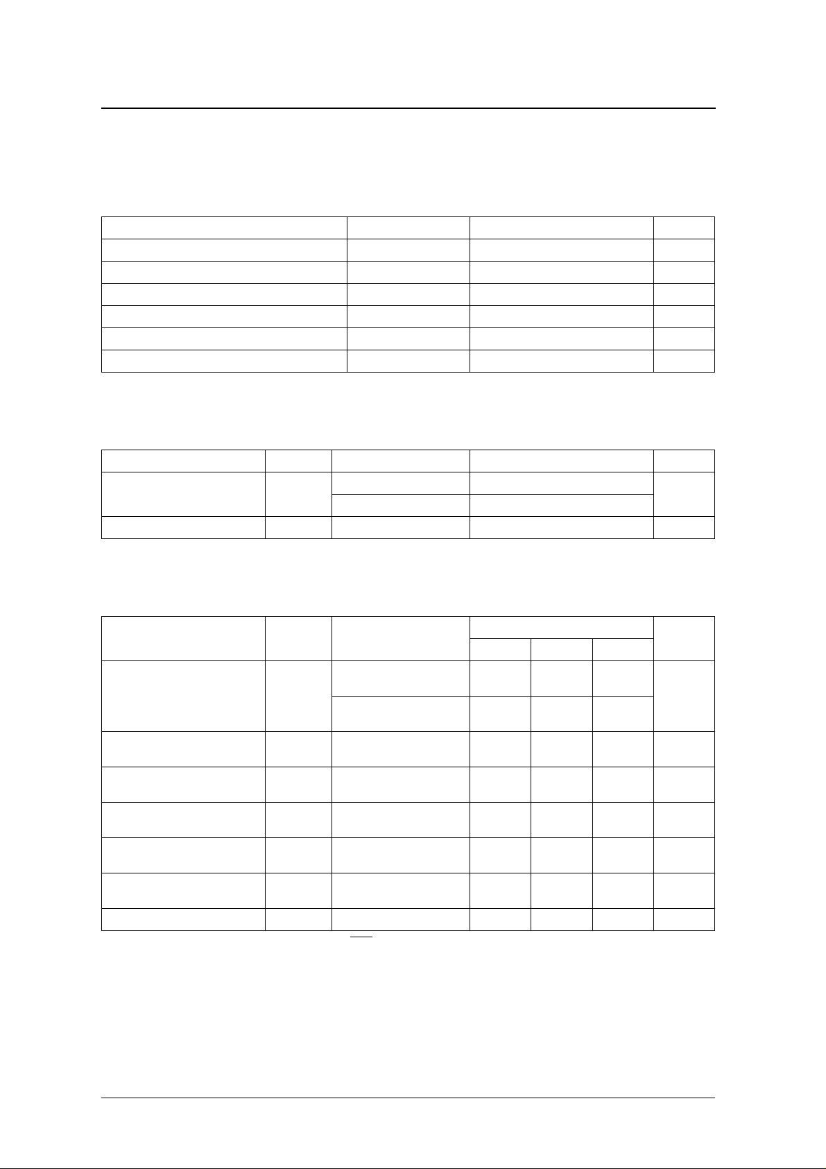
SPECIFICATIONS
Absolute Maximum Ratings
V
= 0 V
SS
Parameter Symbol Rating Unit
Supply voltage range V
Input voltage range V
Power dissipation P
Storage temperature range T
Soldering temperature T
Soldering time t
Recommended Operating Conditions
µ
−
µ
µ
DD
IN
D
stg
sld
sld
0.3 to 7.0 V
0.3 to V
+ 0.3 V
DD
250 mW
40 to 125
260
10 s
C
C
V
= 0 V
SS
Parameter Symbol Condition Rating Unit
76.8 kHz system clock 1.2 to 3.5
Supply voltage range V
Operating temperature range T
DD
opr
153.6 kHz system clock 2.0 to 3.5
DC Characteristics
V
= 1.2 to 3.5 V, V
DD
Parameter Symbol Condition
Consumption current
HIGH-level input voltage
(all inputs)
LOW-level input voltage
(all inputs)
HIGH-level output voltage
(all outputs except XTN)
LOW-level output voltage
(all outputs except XTN)
Input leakage current
(all inputs except XT)
Standby supply current I
1. The consumption current is slightly higher when RST is going LOW.
SS
1
= 0 V, T
= − 20 to 70 ° C unless otherwise noted
a
XT = 76.8 kHz,
V
= 3.5 V
I
V
V
V
V
I
DDS
DD
IH
IL
OH
OL
IL
DD
XT = 153.6 kHz,
V
= 3.5 V
DD
I
= − 20 µ A, V
OH
I
= 20 µ A, V
OH
V
= V
IN
DD
T
= 25 ° C – – 1.0
a
= 2.0 V V
DD
= 2.0 V – – 0.1 V
DD
or V
SS
20 to 70
Rating
min typ max
– 20.0 30.0
– 25.0 35.0
0.8V
DD
– – 0.2V
0.1 – – V
DD
––V
DD
–– ± 1.0
V
Unit
A
V
A
A
NIPPON PRECISION CIRCUITS—3
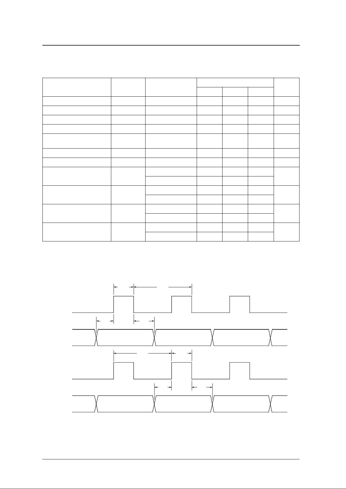
AC Characteristics
V
= 1.2 to 3.5 V, V
DD
SS
= 0 V, T
SM8211M
= − 20 to 70 ° C unless otherwise noted
a
µ
µ
µ
µ
−
µ
µ
µ
µ
µ
Parameter Symbol Condition
TX-CLK pulsewidth t
TX-CLK pulse cycle t
TX-DATA setup time t
TX-DATA hold time t
XT pulse frequency t
XT pulse duty cycle D
BREAK pulsewidth t
RX-CLK pulse cycle
RX-CLK pulsewidth
RX-DATA lead time
RX-DATA hold time
1
1
1
1
PWTX
CYTX
STX
HTX
CYXT
PWBR
t
CYRX
t
PWRX
t
SRX
t
HRX
XT
512 bps – 1953 –
1200 bps – 833 –
512 bps – 124 –
1200 bps – 52 –
512 bps – 1341 –
1200 bps – 573 –
512 bps – 488 –
1200 bps – 208 –
1. Internal digital PLL operation is subject to some change.
Rating
Unit
min typ max
13 – 100
450 – –
1.0 – –
1.0 – –
250 ppm
76.8 or
153.6
+250 ppm kHz
s
s
s
s
25–75%
13 – –
s
s
s
s
s
AC timing
TX-CLK
TX-DATA
RX-CLK
RX-DATA
t
PWTX
t
STX
t
CYRX
t
CYTX
t
HTX
t
PWRX
t
SRX
t
HRX
NIPPON PRECISION CIRCUITS—4
SM8211M
FUNCTIONAL DESCRIPTION
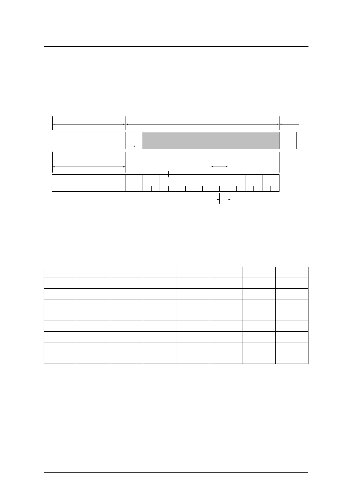
Receive Format
The receive format conforms to CCIR RPC No. 1
(POCSAG).
Preamble
SC SC
1st batch
2nd and
successive
batches
Continuous 576-bit "1,0" bit pattern
... 1 0 1 0 1 0 1 0 1 0 ...
Sync code word
Frame number
0SC 1234567
1 code word (32 bits)
1 frame (= 2 code words)
Figure 1. Receive signal format
Sync signal (SC)
The sync signal is a continuous code word in the
received signal, used for word synchronization. It
even-parity bit, making a 32-bit signal. The sync
code word pattern is shown in table 1.
comprises 31 bits in an M-series bit pattern plus one
Table 1. Sync code word
Bit number Bit value Bit number Bit value Bit number Bit value Bit number Bit value
1091170251
2 1101180261
3 1110190270
4 1121201281
5 1130210291
6 1140221300
7 0151230310
8 0160241320
NIPPON PRECISION CIRCUITS—5
SM8211M
Code words (address and message signals)
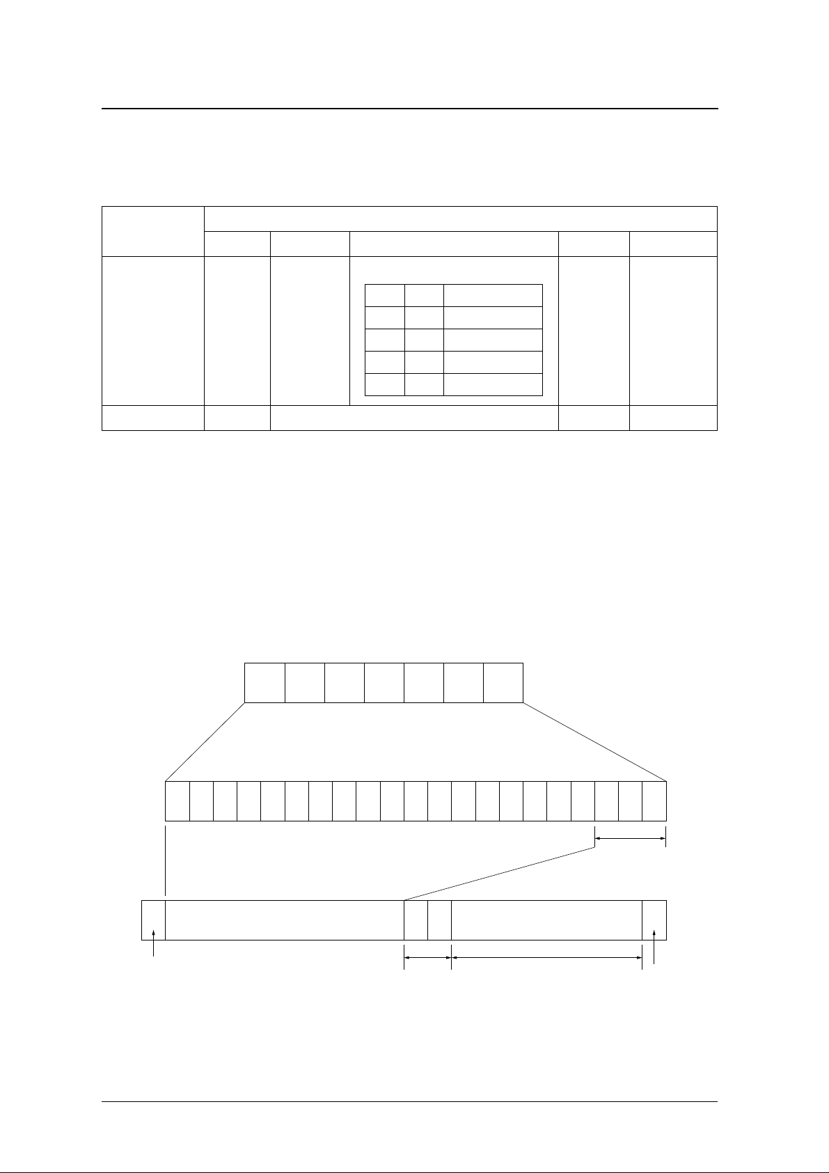
Each code word comprises 32 bits as shown in table 2.
Table 2. Code word format
Code word
1 (MSB)
1
2 to 19
2
20, 21
2
22 to 31
3
32 (LSB)
4
Function bits
20 21 Function
0 0 A call
Bit number
Address signal 0 Address bits
0 1 B call
Check bits Even-parity bit
1 0 C call
1 1 D call
Message signal 1 Message bits Check bits Even-parity bit
1. The MSB is the address/message code word control bit. It is 0 for an address signal, and 1 for a message signal.
2. Bits 2 to 21 contain the address or message information.
3. Bits 22 to 31 are BCH(31,21) f ormat generated check bits , where BCH(n,k) = BCH(w ord length, number of information bits).
4. The LSB is an even-parity bit for bits 1 to 31.
Call number to call sign conversion
This conversion expands a 7-digit decimal call number into a 21-bit binary call sign, as shown in figure
2.
bits are the user-defined frame identification pattern,
which is stored in ID-ROM. The two function bits
define which of four call functions is active.
After expansion, the high-order 18 bits are assigned
to bits 2 to 19 (address signal), and the low-order 3
7-digit decimal call
signal (gap code)
MSB LSB
21-bit binary
conversion
Call sign
1 2 3 4 5 6 7 8 9 10 11 12 13 14 15 16 17 18 19 20 21
Flag:
0 = address signal
1 = message signal
1
2 3 4 5 6 7
Bits 2 to 19 (18 bits)
20 21 321 Bits 22 to 31 (10 bits)
Function bits BCH(31,21) generated check bits
Figure 2. Call number to call sign conversion
Frame
identificaton
pattern
Even-parity bit
(for bits 1 to 31)
NIPPON PRECISION CIRCUITS—6

SM8211M
Idle signal (dummy signal)
An idle word can be inserted into either the address
or message signal to indicate that the word contains
no information. The idle word bit pattern is shown in
table 3. Message reception is halted when the
receiver detects an idle word.
In pager systems that send numeric data, the number
of frames varies with the type of message being sent.
In this case, an idle signal is transmitted to indicate
completion of the message.
Table 3. Idle code word
Bit
number
1 0 17 1
2 1 18 1
3 1 19 0
4 1 20 0
5 1 21 0
6 0 22 0
7 1 23 0
8 0 24 1
9 1 25 1
100260
110270
120281
131290
140301
150311
Bit value
Bit
number
Bit value
Battery Saving (BS1, BS2, BS3)
The SM8211M controls the intermittent-duty operation of the RF stage, which reduces battery consumption, and outputs three control signals (BS1, BS2,
BS3). The function each signal controls in each
mode is described below.
■ BS1 (RF-control main output signal)—The RF
stage is active when BS1 is HIGH. The risingedge setup time for receive timing is set by flags
RF0 to RF5 (60 steps). The maximum setup time
is 49.167 ms at 1200 bps, and 115.234 ms at 512
bps.
Note that 3C, 3D, 3E and 3F are invalid settings
for BS1.
■ BS2 (RF-control output signal)—BS2 is used to
control the discharge of the receive signal DC-cut
capacitor. The function of BS2 is determined by
flag BS2, as described below.
• When flag BS2 is 0, pin BS2 goes HIGH
together with BS1 and then goes LOW again
after the BS1 setup time. However, in lock
mode (during address/message reception), it
stays LOW.
• When flag BS2 is 1, pin BS2 goes HIGH during
lock mode sync code receive timing, and preamble mode and idle mode signal receive timing.
■ BS3 (RF-control output signal)—BS3 is used to
control PLL operation when the PLL is used. The
rising-edge setup time for receive timing is set by
flags PL0 to PL5 (60 steps). The maximum setup
time is 50.833 ms at 1200 bps, and 119.141 ms at
512 bps.
Note that 3E and 3F are invalid settings for BS3.
Note also that (BS3 rising-edge setup time) − (BS1
rising-edge setup time) should be ≥ 2.
161321
Receive signal duty factor
During preamble detection, the preamble pattern
(1,0) is recognized at duty factors from 25% (min) to
75% (max) of the (1,0) preamble cycle.
NIPPON PRECISION CIRCUITS—7
 Loading...