NPC SM6781BV Datasheet

preliminary
−∆
SM6781BV
NIPPON PRECISION CIRCUITS INC.
Ni-MH/Ni-Cd Battery Charger IC
OVERVIEW
The SM6781BV is a quick charge control IC for Nickel Metal Hydride (NiMH) and Nickel-Cadmium (NiCd)
rechargeable batteries. Quick charging ends in response to negative delta voltage detection (– ∆ V) and maximum charging time detection functions. Also, quick charge mode is placed on hold if the battery voltage
becomes abnormal, until normal conditions are restored. The SM6781BV requires few external components to
realize a high-stability quick charge battery charger.
FEATURES
■
Ni-MH/Ni-Cd battery quick charge control
■
V and maximum charge time cutoffs
■
15min (typ) −∆ V detection invalid time
■
– 4mV (typ) −∆ V detection accuracy
■
Inhibit function
■
Charge condition LED indicator output
(on, pulsed, off)
■
Low power dissipation standby mode (< 1 µ A)
■
8-pin VSOP package
PINOUT
(Top view)
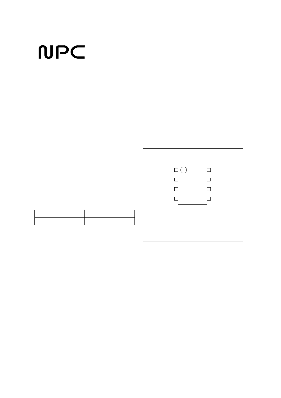
TIME CHGN
LEDN
BATT
INH
NC
ORDERING INFORMATION
Device Package
SM6781BV 8-pin VSOP
VSS
PACKAGE DIMENSIONS
(Unit: mm)
TBD
VDD
NIPPON PRECISION CIRCUITS—1

preliminary
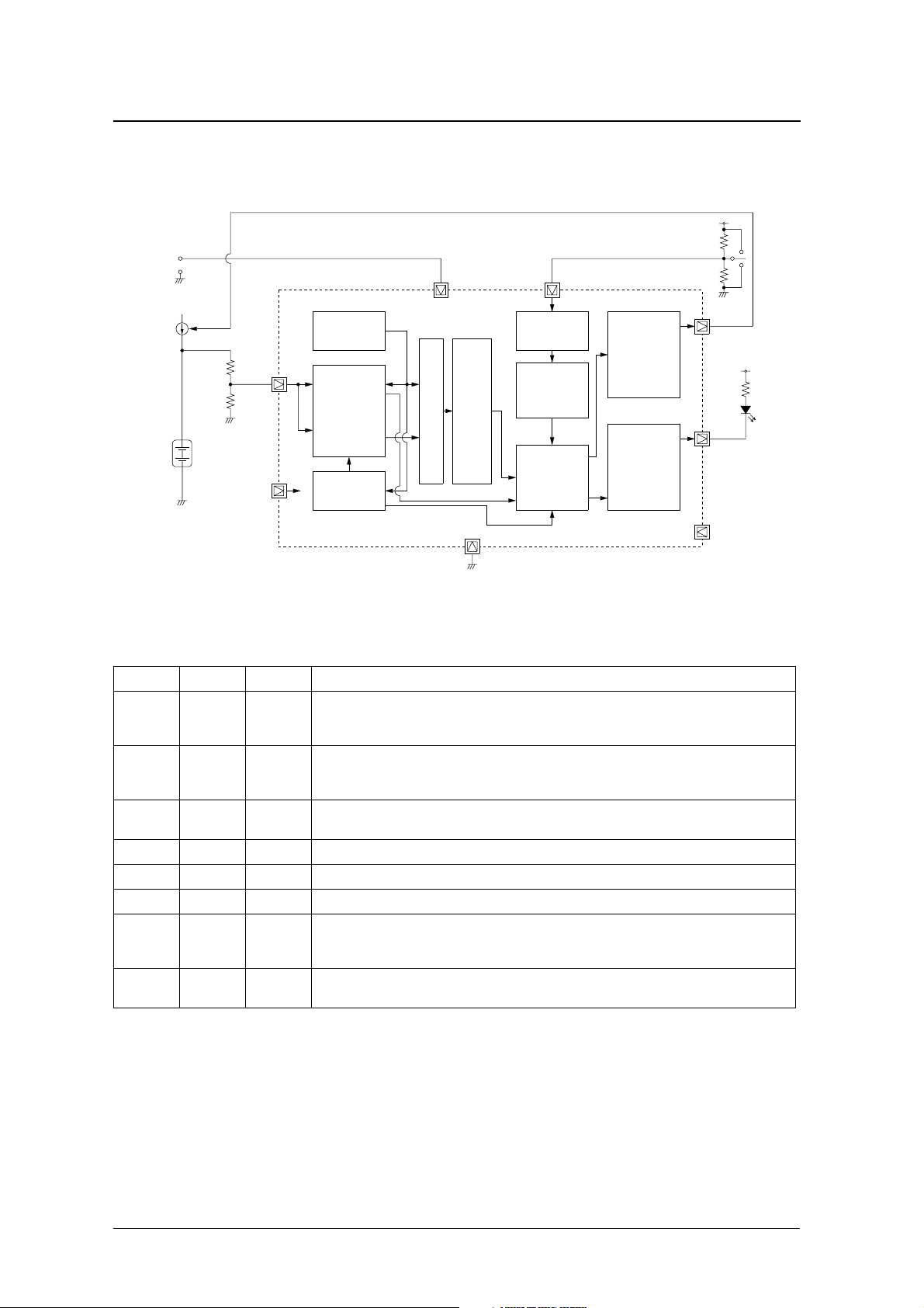
BLOCK DIAGRAM
DC
Input
SM6781BV
VDD
TIMEVDD
Current
Source
Battery
Pack
BATT
INH
Reference
Regulators
Max/Min
Cell-voltage
Check
OSC
A/D
−∆V
Function
Block
VSS
Timer Mode
Selector
Timing Control
Charge Control
PIN DESCRIPTION
Number Name I/O Description
1 TIME I
2 LEDN O
3BATT I
4 VSS – Ground
5 VDD – Supply
6 NC – No connection (must be open)
7INH I
8 CHGN O
Timer mode select input (3-level)
HIGH and LOW levels applied using pull-up and pull-down, respectively. MID-level is applied using a
voltage divider resistor network with voltage VDD/2.
Charge status display LED driver output (open-drain output)
LOW-level output in quick charge mode. 1Hz pulse output when abnormal battery voltage is detected
during quick charge. High impedance when charging finishes.
Battery voltage detector input.
Connect a high-impedance resistor voltage divider between the poles of the battery for voltage detection.
Inhibit input
Charging operation is stopped when HIGH. Charging recommences with the same charging parameters
when INH goes LOW again.
Charge control (open-drain output)
High impedance output when charging current is flowing. LOW-level output when charging current stops.
CHGN
CHG Driver
VDD
Logic
LEDN
LED Driver
Logic
NC
NIPPON PRECISION CIRCUITS—2

preliminary
−
−
−
°
°
SPECIFICATIONS
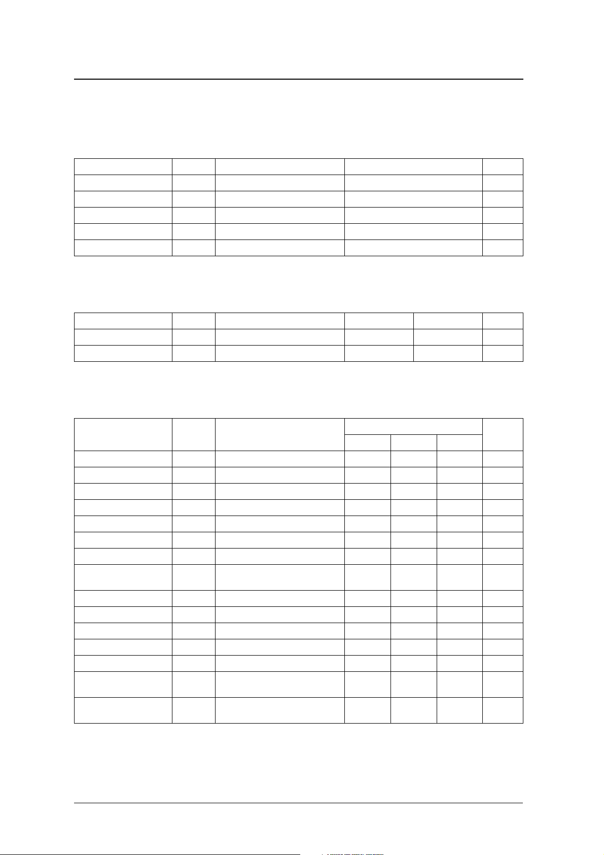
Absolute Maximum Ratings
V
= 0V
SS
Parameter Symbol Condition Rating Unit
Supply voltage range V
Input voltage range V
Storage temperature range T
Operating temperature range T
Power dissipation P
DC Characteristics 1
DD
IN
stg
opr
D
−
−
−
−
SM6781BV
0.3 to 7.0 V
0.3 to 7.0 V
55 to 125
– 25 to 85
150 mW
C
C
V
= 4.0 to 5.5V, V
DD
Parameter Symbol Condition Rating Variation Unit
Minimum battery voltage V
Maximum battery voltage V
= 0V, Ta = 25 ° C
SS
DC Characteristics 2
V
= 4.0 to 5.5V, V
DD
Parameter Symbol Condition
VDD supply voltage V
BATT input voltage V
INH HIGH-level input voltage V
INH LOW-level input voltage V
TIME HIGH-level input voltage V
TIME MID-level input voltage V
TIME LOW-level input voltage V
BATT −∆ V detection voltage
range
LEDN output pulse frequency f
BATT standby voltage V
VDD current consumption I
VDD standby current I
LEDN, CHGN sink current I
INH, TIME input leakage
current
LEDN, CHGN output leakage
current
= 0V, Ta = 0 to 85 ° C unless otherwise noted
SS
MNV
MXV
BATT
V
LED
STB
I
DD
IH1
IL1
IH2
IM
IL2
DET
STB
DD
OL
I
OZ
V
< V
BATT
V
BATT
V
= 5V, no load – – 0.5 mA
DD
V
= 5V, V
DD
V
= V
OL
V
L
INH
charge cutoff or prohibition 0.6 ± 0.2 V
MNV
> V
charge cutoff or prohibition 2.0 ± 0.1 V
MXV
Rating
min typ max
4.0 5.0 5.5 V
0–V
0.7 – – V
– – 0.1 V
V
0.5 – – V
DD
(V
/2) − 0.5 – (V
DD
– – 0.5 V
1–2V
–1–Hz
V
1.5 – V
DD
= V
BATT
+ 0.8V 10 – – mA
SS
= V
= V
TIME
, no load – – 1 µA
DD
to V
SS
DD
– – ± 1 µA
5– –µA
DD
/2) + 0.5 V
DD
0.5 V
DD
Unit
V
NIPPON PRECISION CIRCUITS—3
 Loading...