

preliminary
−
±3 °
10 °
SM6611 series
NIPPON PRECISION CIRCUITS INC.
Miniature High-Precision Temperature Switch IC
OVERVIEW
The SM6611 series are temperature switch ICs that change state (invert) when the chip temperature exceeds a
preset temperature. The switches are designed with temperature hysteresis to prevent unstable output when the
temperature is in the vicinity of the preset temperature.
There are 6 output switching temperatures in the series, available in 2 output configurations, making the
SM6611 series devices ideal for a wide range of applications.
FEATURES
■
2.4 to 12.0V operating supply voltage
■
20 to 100 ° C operating temperature range
■
C temperature accuracy
■
45 to 95 ° C output switch temperatures in 10 ° C
steps
■
C temperature hysteresis
■
30µA (typ) low current consumption
■
Output configuration
• SM6611 × AH open-drain active-LOW output
• SM6611 × BH CMOS active-HIGH output
■
6-pin SOT23-6W package
APPLICATIONS
■
Motherboard overheating protection
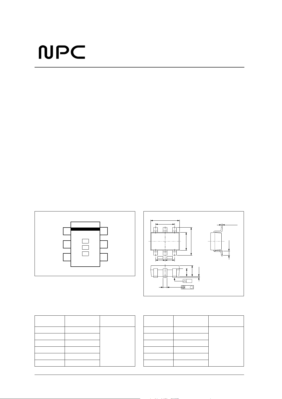
PINOUT
(Top view)
■
Battery-pack temperature protection
PACKAGE DIMENSIONS
(Unit: mm)
2.9 ± 0.2
1.9 ± 0.2
6
VDD
T1
OUT
1
2
3
T2
+ 0.2
+ 0.1
1.8 − 0.1
0.8 ± 0.1
0.12
5
VSS
4
T3
0.95 0.95
0.40 − 0.05
ORDERING INFORMATION
SM6611 × AH series SM6611 × BH series
Device
SM6611AAH 45 ° C
SM6611BAH 55 ° C
SM6611CAH 65 ° C
SM6611DAH 75 ° C
SM6611EAH 85 ° C
SM6611FAH 95 ° C
Output switch
temperature
Output configuration
Open-drain active-
LOW output
Device
SM6611ABH 45 ° C
SM6611BBH 55 ° C
SM6611CBH 65 ° C
SM6611DBH 75 ° C
SM6611EBH 85 ° C
SM6611FBH 95 ° C
Output switch
temperature
0.1
2.8 ± 0.2
1.1 ± 0.1
M
0 to 0.1
Output configuration
+ 0.1
0.125 − 0.05
0.2 min.
CMOS active-HIGH
output
NIPPON PRECISION CIRCUITS—1
preliminary
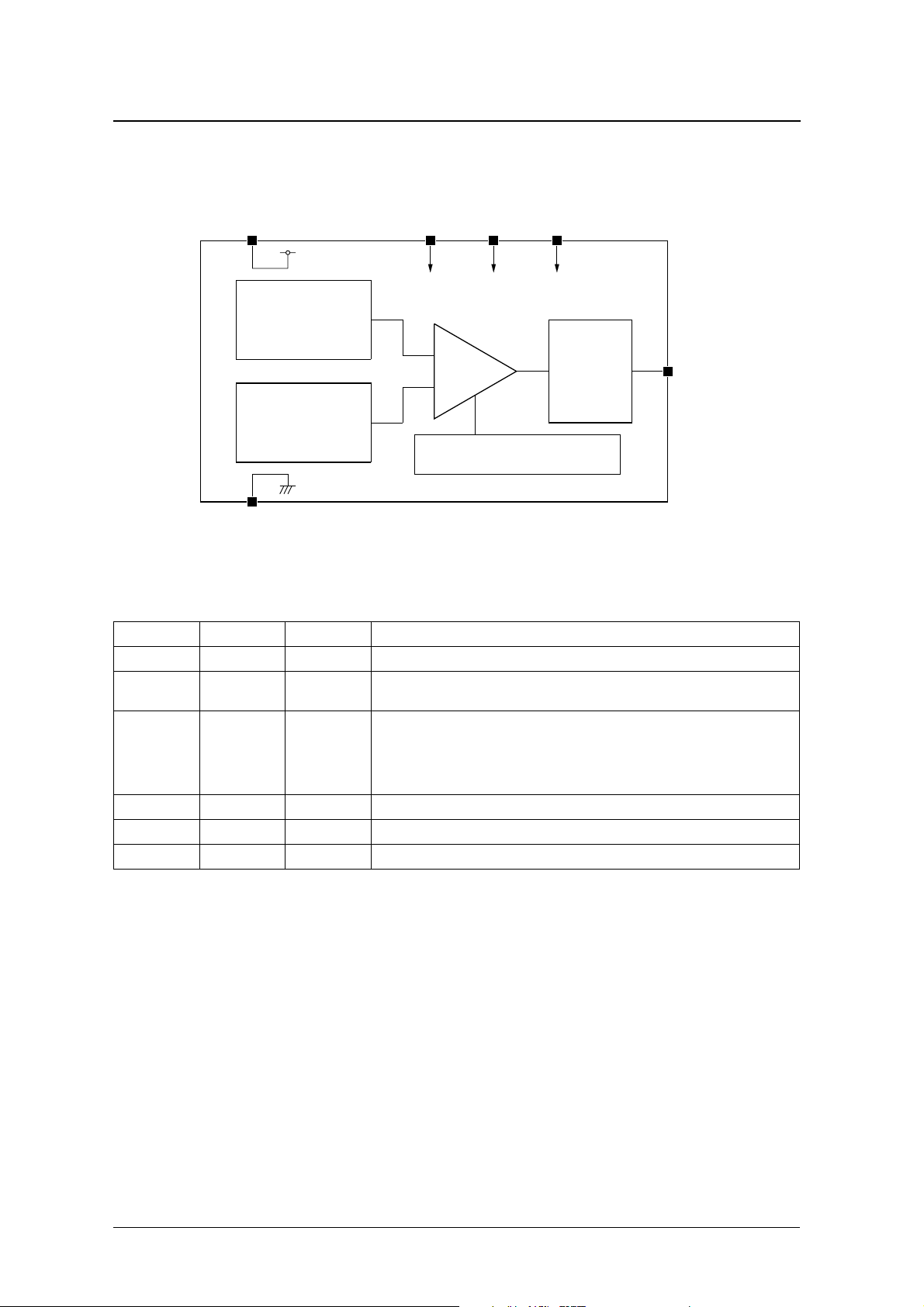
BLOCK DIAGRAM
SM6611 series
VDD
Output inverting
temperature detect
Reference
temperature sensor
VSS
PIN DESCRIPTION
Number Name I/O Description
1 VDD – Supply voltage
2T1–
3 OUT O
4 T3 – Test pin 3. This pin is used for test purposes by NPC. Connect to VSS for normal operation.
5 VSS – Ground
6 T2 – Test pin 3. This pin is used for test purposes by NPC. Connect to VSS for normal operation.
TEST1
Test pin 1. This pin is used for test purposes by NPC. It has a built-in pull-up resistor. Leave
open for normal operation.
Output.
SM6611 × AH: Open-drain output. A pull-up resistor of 100k Ω should be connected to this
pin. Goes LOW when the switch preset temperature is exceeded.
SM6611 × BH: CMOS output. Goes LOW to HIGH when the switch preset temperature is
exceeded.
TEST2 TEST3
Comparator
Hysteresis control
Output
buffer
OUT
NIPPON PRECISION CIRCUITS—2

preliminary
SPECIFICATIONS
Absolute Maximum Ratings
V
= 0V
SS
Parameter Symbol Rating Unit
Supply voltage range V
Power dissipation P
Storage temperature range T
Recommended Operating Conditions
V
= 0V
SS
Parameter Symbol Rating Unit
Supply voltage range V
Operating temperature range T
DD
STG
DD
OPR
−
−
° C
SM6611 series
D
−
° C
−
−
∆
−
0.3 to 15 V
2.5 mW
40 to 125
2.4 to 12 V
20 to 100
DC Characteristics
V
= 2.4 to 12V, V
DD
Parameter Symbol Condition
Supply voltage V
Current consumption I
LOW-level output voltage V
HIGH-level output voltage V
Open-drain output maximum voltage V
Open-drain output leakage current I
Output switch temperature accuracy
Hysteresis temperature T
= 0V, Ta = − 20 to 100 ° C unless otherwise noted
SS
DD
DD
OL
OH
OMAX
LEAK
T
HYST
Rating
min typ max
2.4 – 12 V
– 30 100 µA
I
= 1mA, V
SINK
I
= 3mA, V
SINK
CMOS output (SM6611 × BH),
I
SOURCE
Open-drain output (SM6611 × AH) – – 12 V
V
= 2.4V, V
DD
45 to 95 ° C
TH
> 2.4V – – 0.3 V
DD
> 4V – – 0.4 V
DD
V
1.0 – – V
= 0.5mA, V
= 12V, (SM6611 × AH)
OUT
DD
> 2.4V
DD
1 – +1 µA
3–+3 ° C
–10– ° C
Unit
NIPPON PRECISION CIRCUITS—3

preliminary
SM6611 series
NIPPON PRECISION CIRCUITS INC. reserves the right to make changes to the products described in this data sheet in order to
improve the design or performance and to supply the best possible products. Nippon Precision Circuits Inc. assumes no responsibility for
the use of any circuits shown in this data sheet, conveys no license under any patent or other rights, and makes no claim that the circuits
are free from patent infringement. Applications for any devices shown in this data sheet are for illustration only and Nippon Precision
Circuits Inc. makes no claim or warranty that such applications will be suitable for the use specified without further testing or modification.
The products described in this data sheet are not intended to use for the apparatus which influence human lives due to the failure or
malfunction of the products. Customers are requested to comply with applicable laws and regulations in effect now and hereinafter,
including compliance with export controls on the distribution or dissemination of the products. Customers shall not export, directly or
indirectly, any products without first obtaining required licenses and approvals from appropriate government agencies.
NIPPON PRECISION CIRCUITS INC.
4-3, Fukuzumi 2-chome
Koto-ku, Tokyo 135-8430, Japan
Telephone: +81-3-3642-6661
NIPPON PRECISION CIRCUITS INC.
Facsimile: +81-3-3642-6698
http://www.npc.co.jp/
Email: sales
npc.co.jp
@
NP0022AE 2001.02
NIPPON PRECISION CIRCUITS—4
 Loading...