NPC SM5882AS, SM5883AS, SM5883BS, SM5885CS Datasheet

Σ
Σ∆
Σ∆
DECO SM588 × series
NIPPON PRECISION CIRCUITS INC.
Audio 3rd-order Σ∆ D/A Converter
OVERVIEW
The Σ DECO SM588 × series, fabricated using NPC’s Molybdenum-gate CMOS process, are D/A converter ICs
for digital audio, that provide all the basic converter functions in miniature 8-pin packages. They each feature
built-in 8-times oversampling digital filter, Σ∆ jitter-compensated D/A converter, and post-analog lowpass filter converter stages required for digital audio. They can sample at up to 96kHz for 16 or 24-bit input word
length. A type with built-in deemphasis filter is also available for applications requiring deemphasis.
FEATURES
3-wire Input
■
2-channel stereo configuration
■
256fs, 384fs, or 512fs system clock (applied by
product / version)
■
Input format
3-wire serial, MSB first, rear-packed
16 or 24-bit (applied by product / version)
■
8-times oversampling digital filter
• 32 dB stopband attenuation
• ±0.05 dB passband ripple
■
2-channel D/A converter
• 3rd-order noise shaper
• Oversampling operation
■
3rd-order post-analog lowpass filter
■
4.5 to 5.5 V supply voltage
■
8-pin SOP
■
Molybdenum-gate CMOS process
2-wire Input with Deemphasis Filter
■
2-channel stereo configuration
■
256fs, 384fs, or 512fs system clock (applied by
product / version)
■
Input format
2-wire serial, MSB first, rear-packed
16 or 24-bit (applied by product / version)
■
Deemphasis filter (fs = 44.1 kHz sample rate)
■
8-times oversampling digital filter
• 32 dB stopband attenuation
• ±0.05 dB passband ripple
■
2-channel D/A converter
• 3rd-order noise shaper
• Oversampling operation
■
3rd-order post-analog lowpass filter
■
4.5 to 5.5 V supply voltage
■
8-pin SOP
■
Molybdenum-gate CMOS process
APPLICATIONS
■
Audio equipment
PINOUTS
3-wire input 2-wire input with built-in deemphasis filter
CLK
1
4
5
88
8
5
DATA
BCKI
LRCI
ORDERING INFORMATION
Device Package
SM5882AS
SM5883AS
SM5883BS
SM5885CS
LO
VDD
VSS
RO
8-pin SOP
DATA
DEEM
LRCI
CLK
1
5
88
4
NIPPON PRECISION CIRCUITS—1
LO
8
VDD
VSS
RO
5

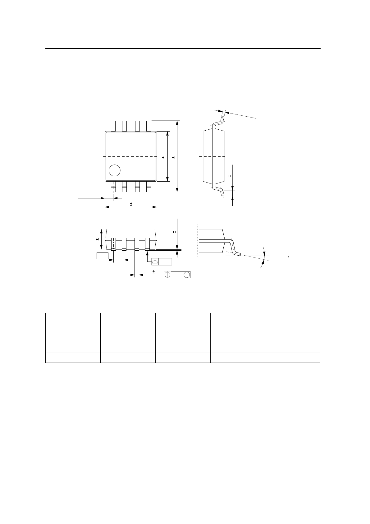
PACKAGE DIMENSIONS
(Unit : mm)
Weight : 0.07g
SM588 × series
4.4 0.2
6.2 0.3
0.15
+
−
0.05
0.1
0.4 0.2
0.695typ
5.2 0.3
0.05 0.05
1.5 0.1
1.27
0.10
0.4 0.1
0.12
M
SERIES LINEUP
Device Input length Type Pin 2 function Master clock
SM5882AS 16 2-wire input Deemphasis control 384fs
SM5883AS 16 3-wire input Bit clock input 384fs
SM5883BS 16 3-wire input Bit clock input 256fs
SM5885CS 24 3-wire input Bit clock input 512fs
0 to 10
NIPPON PRECISION CIRCUITS—2

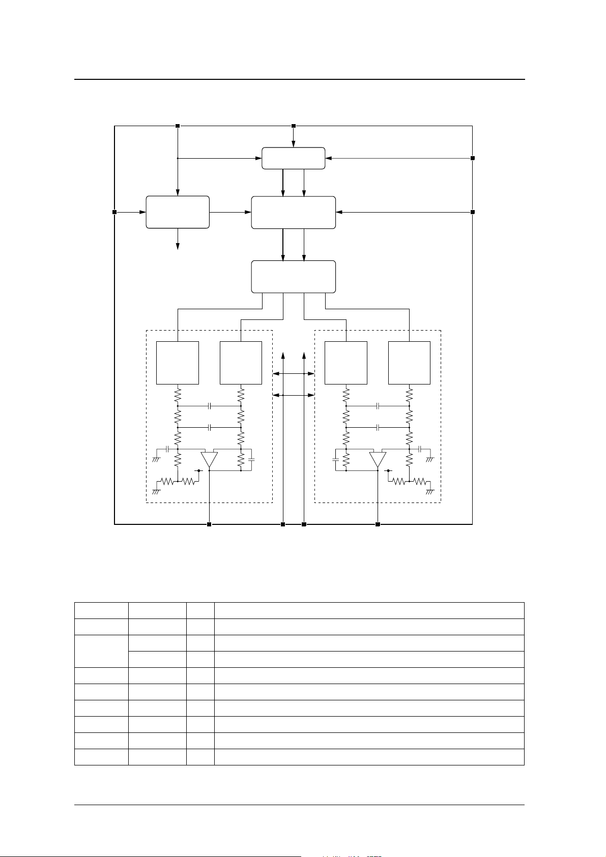
BLOCK DIAGRAM
LRCI DATA
SM588 × series
CLK
Timing
control
9 Level
DEM DAC
9 Level
DEM DAC
Input interface
LR
Filter & attenuation
operation block
LR
Noise shaper
operation block
9 Level
DEM DAC
BCKI*
DEEM**
9 Level
DEM DAC
+−
LO VSS RO
* : Not available for 2-wire input type
** : Not available for 3-wire input type
VDD
+−
PIN DESCRIPTION
Number Name I/O Description
1 DATA I Serial data input
1
2
3 LRCI I Sample rate (fs) clock input. Left-channel input when HIGH, and right-channel input when LOW.
4 CLK I External clock input
5 RO O Right-channel analog output
6 VSS – Ground
7 VDD – Supply
8 LO O Left-channel analog output
BCKI
DEEM
2
I Bit clock input
I Deemphasis ON/OFF control (44.1 kHz, ON when HIGH)
1. 3-wire type
2. 2-wire type with built-in deemphasis filter
NIPPON PRECISION CIRCUITS—3

SM588 × series
SPECIFICATIONS
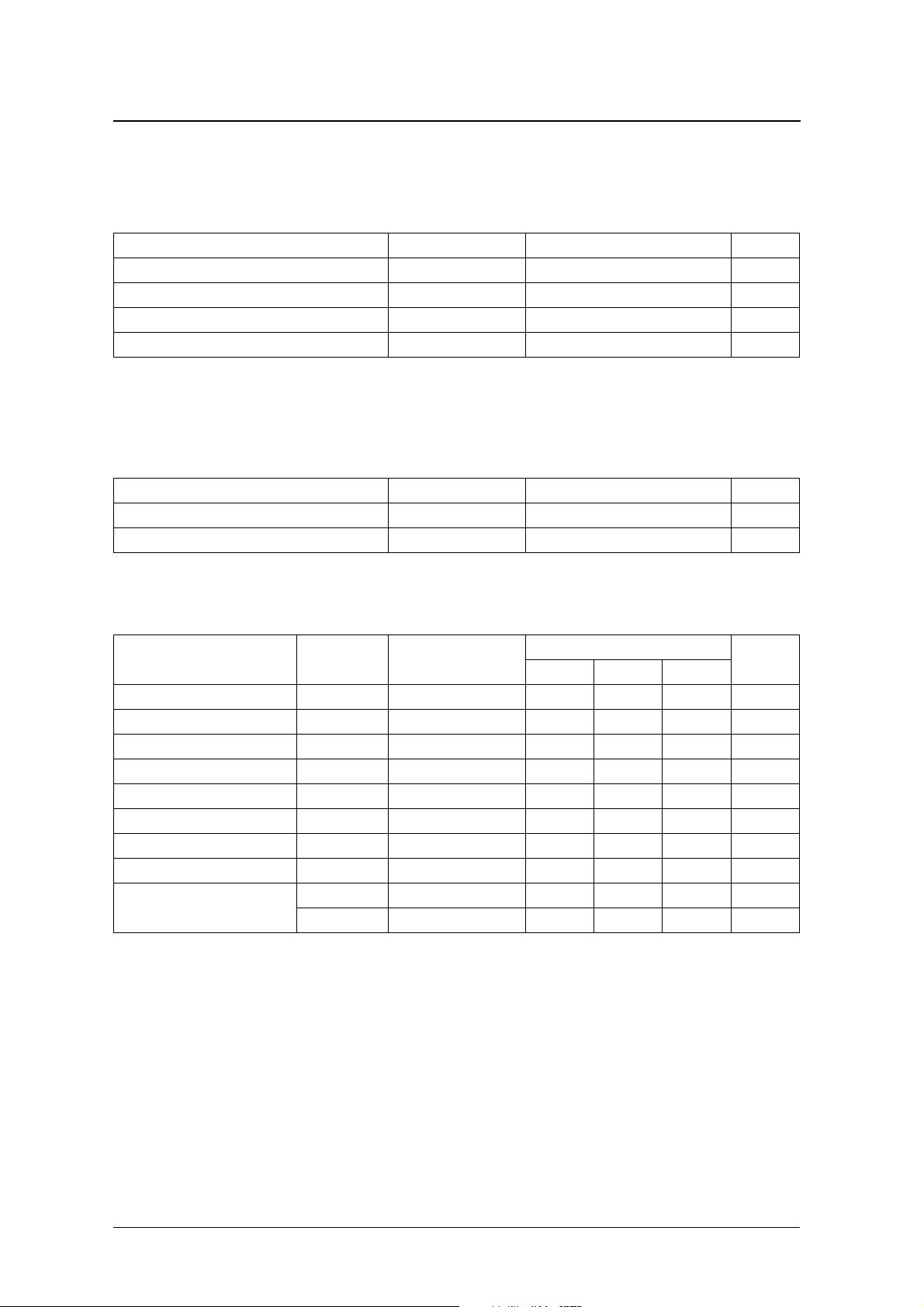
Absolute Maximum Ratings
V
= 0 V
SS
Parameter Symbol Rating Unit
Supply voltage range V
Input voltage range
Storage temperature range T
Power dissipation P
1. All inputs
Also applicable during supply switching.
Recommended Operating Conditions
1
−
−
+
−
°
−
° C
0.3 to 7.0 V
V
SS
0.3 to V
0.3 V
DD
55 to 125
300 mW
C
V
STG
DD
IN
D
V
= 0 V
SS
Parameter Symbol Rating Unit
Supply voltage V
Operating temperature T
DD
OPR
DC Characteristics
V
= 4.5 to 5.5 V, V
DD
Parameter Symbol Condition
Current consumption
1
CLK HIGH-level input voltage V
CLK LOW-level input voltage V
CLK AC-coupled input voltage V
HIGH-level input voltage
LOW-level input voltage
CLK HIGH-level input current I
CLK LOW-level input current I
Input leakage current
1. V
= 5 V, CLK clock input frequency f
DD
Input data: NPC pattern.
2
2. Pins BCKI (3-wire type), DEEM (2-wire type with deemphasis filter), DATA, LRCI
= 0 V, Ta = − 40 to 85 ° C
SS
2
2
V
= 16.9344 MHz (384fs type)/11.2896 MHz (256fs type)/22.5792MHz (512fs type), no output load.
CLK
I
DD
INAC
V
I
LH
I
IH1
IL1
IH2
IL2
IH
IL
LL
Clock input 0.7V
Clock input – – 0.3V
V
= V
IN
DD
V
= 0 V 20 62 170 µA
IN
V
= V
IN
DD
V
= 0 V – – 1.0 µA
IN
4.5 to 5.5 V
40 to 85
Rating
min typ max
– 12.5 25.0 mA
DD
––V
DD
0.7 – – V
0.5V
DD
– – 0.2V
––V
DD
20 62 170 µA
– – 1.0 µA
Unit
V
p-p
V
NIPPON PRECISION CIRCUITS—4

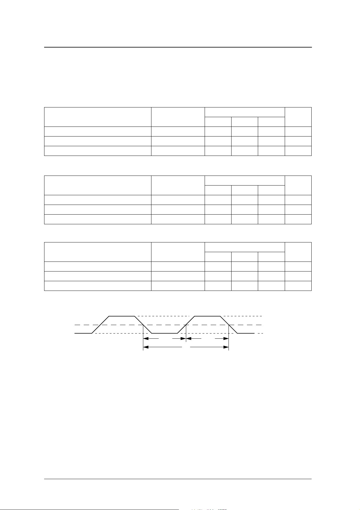
AC Digital Characteristics
V
= 4.5 to 5.5 V, V
DD
System clock (CLK)
256fs type
= 0 V, Ta = − 40 to 85 ° C
SS
SM588 × series
Parameter Symbol
HIGH-level clock pulsewidth t
LOW-level clock pulsewidth t
Clock pulse cycle t
384fs type
Parameter Symbol
HIGH-level clock pulsewidth t
LOW-level clock pulsewidth t
Clock pulse cycle t
512fs type
Parameter Symbol
HIGH-level clock pulsewidth t
LOW-level clock pulsewidth t
Clock pulse cycle t
CWH
CWL
XI
CWH
CWL
XI
CWH
CWL
XI
Rating
Unit
min typ max
20.0 – 125 ns
20.0 – 125 ns
40.0 – 250 ns
Rating
Unit
min typ max
13.15 – 125 ns
13.15 – 125 ns
26.3 – 250 ns
Rating
Unit
min typ max
10 – 125 ns
10 – 125 ns
20 – 250 ns
CLK
t
CWL
V
IH1
0.5V
DD
V
t
CWH
t
XI
NIPPON PRECISION CIRCUITS—5
IL1
 Loading...