∑∆
SM5879AV
NIPPON PRECISION CIRCUITS INC.
3rd-order Σ∆ , 2-channel D/A Converter
OVERVIEW
The SM5879AV is a 3rd-order ∑∆ , two-channel D/A
convertor LSI for digital audio reproduction equipment. This device incorporate NPC's molybdenumgate CMOS technology and incorporates an 8-times
oversampling digital filter and analog 3rd-order ∑∆
post-converter low-pass filters.
The SM5879AV also incorporates built-in digital
bass boost and deemphasis filters, an attenuator, and
soft mute function. Low-voltage operation is also
supported.
This device features a compact 24-pin VSOP package and a D/A converter that provides both compact
size and low power consumption.
FEATURES
■
2.7 to 3.3 V operating supply voltage
■
44.1 kHz sampling frequency
■
16.9344 MHz (384fs) system clock
■
Built-in crystal oscillator circuit
■
16-bit, MSB first, rear-packed serial data input
format ( ≤ 64 fs bit clock)
■
8-times oversampling digital filter
• 32 dB stopband attenuation
• +0.05 to -0.05 dB passband ripple
■
Deemphasis filter operation
• 36 dB stopband attenuation
• -0.09 to +0.23 dB deviation from ideal deemphasis filter characteristics
■
Attenuator
• 7-bit attenuator (128 steps) set by microcontroller
■
Soft mute function set by parallel setting
• (approximately 1024/fs total muting time)
■
Mono setting
• Left or right channel mono selectable by microcontroller
■
Built-in infinity-zero detection circuit
■
, two-channel D/A converter
• 3rd-order noise shaper
• 32fs oversampling
■
Built-in 3rd-order post-converter low-pass filters
■
24-pin VSOP package
■
Molybdenum-gate CMOS process
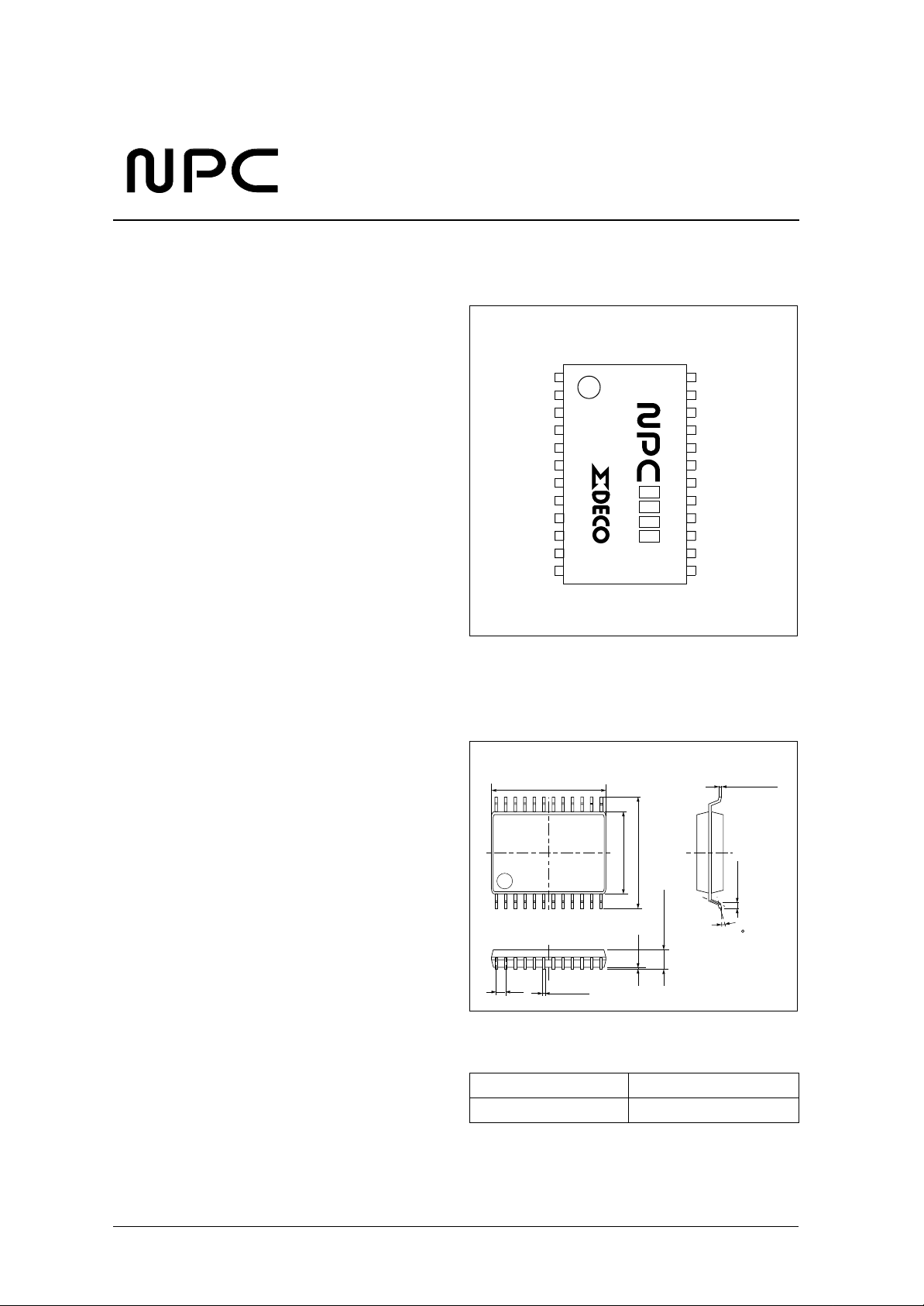
PINOUT
(TOP VIEW)
DVDD
TEST
P / M
AVDDR
RO
AVSSR
TO1
AVSSL
LO
AVDDL
MUTEO
DVSS
1
SM5
879
A
V
12 13
24
PACKAGE DIMENSIONS
Unit: mm
24-pin VSOP
7.8 ± 0.1
5.6 ± 0.1
7.6 ± 0.2
−0.1
+0.2
1.25
0.1 ± 0.1
+0.1
0.22
0.65
−0.05
ORDERING INFOMATION
Device Package
SM5879AV 24pin VSOP
LRCI
BCKI
DI
BB2 / BBON
BB1 / MDT
DEEM / MCK
MUTE / MLEN
XVDD
XTO
XTI
XVSS
CKO
+ 0.05
0.15 − 0.02
0.5 ± 0.2
0 to 10
NIPPON PRECISION CIRCUITS—1

−
−
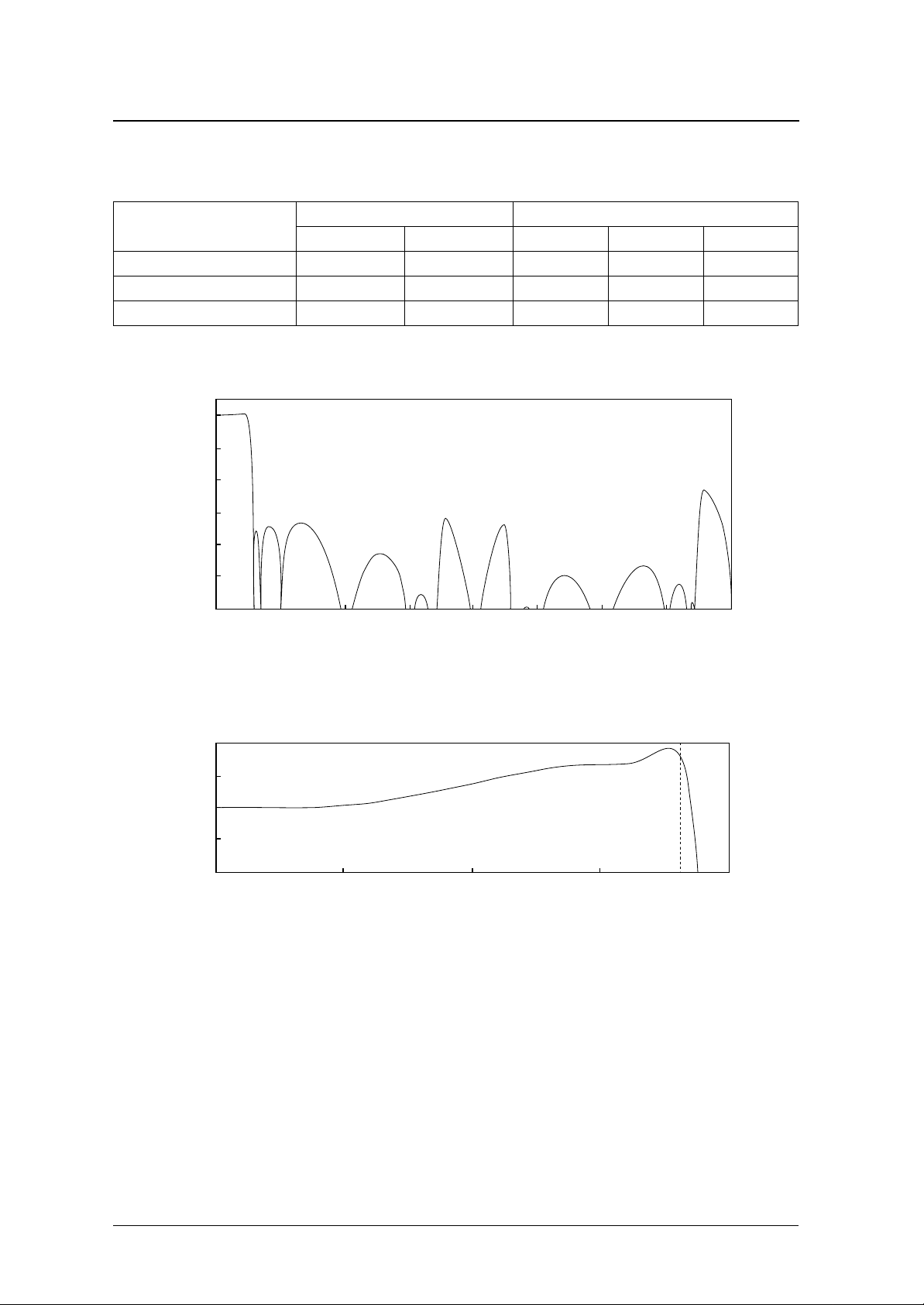
Theoretical Filter Characteristics
Deemphasis OFF overall characteristics
SM5879AV
Parameter
Passband ripple 0 to 0.4535fs 0 to 20.0 kHz
Stopband attenuation 0.5465fs to 7.4535fs 24.1 to 328.7 kHz 32 – –
Built-in analog LPF compensation 0.4535fs 20.0 kHz –
Frequency band Attenuation (dB)
f @ fs = 44.1 kHz min typ max
0.05 – +0.05
0.34 –
Overall frequency characteristic (deemphasis OFF)
0
10
20
30
Gain(dB)
40
50
60
0.0 1.0 2.0 3.0 4.0 5.0 6.0 7.0 8.0
Frequency (Fs)
Passband characteristic (deemphasis OFF)
0.0
0.2
0.4
Gain(dB)
0.6
0.8
0.000 0.125 0.250 0.375 0.500
0.4535
Frequency (Fs)
NIPPON PRECISION CIRCUITS—2

−
−
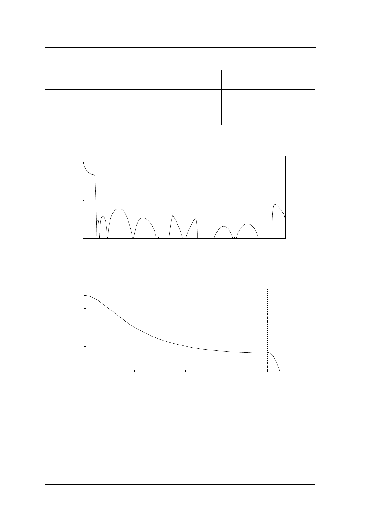
Deemphasis ON overall characteristics
SM5879AV
Parameter
Deviation from ideal deemphasis filter
characteristics
Stopband attenuation 0.5465fs to 7.4535fs 24.1 to 328.7 kHz 36 – –
Built-in analog LPF compensation 0.4535fs 20.0 kHz –
0 to 0.4535fs 0 to 20.0 kHz
Frequency band Attenuation (dB)
f @ fs = 44.1 kHz min typ max
0.09 – +0.23
0.34 –
Overall frequency characteristic (deemphasis ON)
0
10
20
30
Gain(dB)
40
50
60
0.0 1.0 2.0 3.0 4.0 5.0 6.0 7.0 8.0
Frequncy (Fs)
Passband characteristic (deemphasis ON)
0
2
4
6
8
Gain(dB)
10
12
0.000 0.125 0.250 0.375 0.500
0.4535
Frequncy (Fs)
NIPPON PRECISION CIRCUITS—3

SM5879AV
PIN DESCRIPTION
Number Name I/O Description
1 DVDD I- Digital supply pin.
2 TEST I Input for testing LSI. Test mode when HIGH.
3 P/M I Parallel/microcontroller setting selection pin. Parallel setting when HIGH.
4 AVDDR - Right-channel analog supply pin.
5 RO O Right channel analog output pin.
6 AVSSR - Right-channel analog ground pin.
7 TO1 O Test mode output. Normally LOW.
8 AVSSL - Left-channel analog ground pin.
9 LO O Left-channel analog output pin.
10 AVDDL O Left-channel analog supply pin.
11 MUTEO O Infinity-zero detection output
12 DVSS - Digital ground pin
13 CKO O Oscillator clock output. 16.9344 MHz.
14 XVSS - Crystal oscillator ground pin
15 XTI I Crystal oscillator or 16.9344-MHz external clock input pin
16 XTO O Crystal oscillator output pin
17 XVDD - Crystal oscillator supply pin
18 MUTE/ MLEN I
19 DEEM/ MCK I
20 BB1/ MDT I
21 BB2/ BBON IO
22 DI I Serial data input pin
23 BCKI I Bit clock input pin
24 LRCI I Sample rate clock (fs) input pin. Left channel when HIGH, and right channel when LOW.
P/M=H; soft mute control pin. Mute is active when HIGH.
P/M=L; microcontroller interface clock
P/M=H; deemphasis control pin. Deemphasis is ON when HIGH.
P/M=L; microcontroller interface clock
P/M=H; bass boost setting switch pin 1
P/M=L; microcontroller interface serial data
P/M=H; bass boost setting switch pin 2
P/M=L; bass boost detection output
NIPPON PRECISION CIRCUITS—4

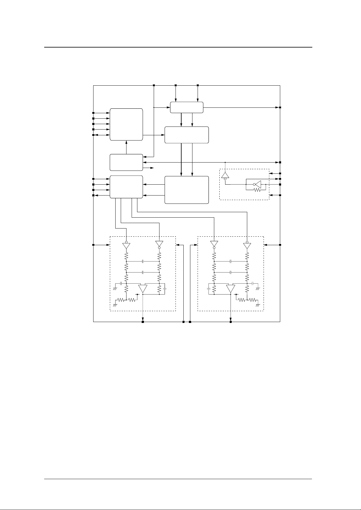
BLOCK DIAGRAM
SM5879AV
LRCI DIBCKI
P /M
MUTE / MLEN
DEEM / MCK
BB1 / MDT
BB2 / BBON
DVSS
DVDD
TEST
TO1
AVDDL
Microcontroller
interface
Timing
control
PWM data
generation block
Filter & attenuation
L
R
Input interface
LR
operation block
LR
Noise shaper
operation block
MUTEO
CKO
XVSS
XTO
XTI
XVDD
AVDDR
+−
LO RO
AVSSRAVSSL
+−
NIPPON PRECISION CIRCUITS—5

SM5879AV
SPECIFICATIONS
Absolute Maximum Ratings
DV
= AV
SS
Supply voltage range DV
Input voltage range
XTI input voltage range V
Storage temperature range T
Power dissipation P
Soldering temperature T
Soldering time t
1. Pins TEST, P/ M, MUTE/ MLEN, DEEM/ MCK, BB1/ MDT, BB2/ BBON, DI, BCKI, LRCI
Also applicable during supply switching.
SSL
= AV
SSR
= XV
= 0 V, AV
SS
DD
= AV
DDL
= AV
DDR
Parameter Symbol Rating Unit
, AV
, XV
DD
DD
DD
1
V
IN1
IN
stg
D
sld
sld
−
−
+
−
+
−
°
°
−
−
−
−
−
−
−
°
0.3 to 7.0 V
DV
XV
SS
SS
0.3 to DV
0.3 to XV
55 to 125
0.3 V
DD
0.3 V
DD
C
250 mW
255
C
10 s
Recommended Operating Conditions
DV
= AV
SS
Supply voltage range DV
Supply voltage variation
Operating temperature range T
note) Since DVDD, XVDD, AVDDL, and AVDDR are connected via the LSI base board, current may flow if potential difference occurs among them.
SSL
= AV
SSR
= XV
= 0 V, AV
SS
DD
= AV
DDL
= AV
DDR
Parameter Symbol Rating Unit
, AV
DV
DV
XV
DV
DV
XV
, XV
DD
DD
DD
XV
DD
DD
DD
SS
SS
,
DD
AV
,
DD
AV
,
DD
XV
,
SS
AV
,
SS
AV
SS
SS
opr
2.7 to 3.3 V
±0.1 V
20 to 70
C
NIPPON PRECISION CIRCUITS—6
 Loading...