

Σ
DECO SM5865CM
NIPPON PRECISION CIRCUITS INC.
OVERVIEW
The SM5865CM is a 24-bit input D/A converter LSI
for high-quality digital audio equipment. It comprises newly developed DEM (dynamic element
matching) circuits, 3rd-order Σ∆ noise shaper and
31-level quantizer to realize super low total harmonic distortion and wide dynamic range. Also, the
device is widely reduced residual quantization noise
up to high-frequency bandwidth in the audio band so
the order of the required final-stage analog lowpass
filter can be reduced, making it ideal for application
with high-frequency sampling format. The output
stage employs differential current outputs for highaccuracy analog signals, with appropriate lowpass
filtering of the output signal. This device can be used
in combination with an 8-times oversampling digital
filter of SM5847AF and others like that for the com-
patibility with 192kHz sampling format.
FEATURES
D/A Converter for Digital Audio
PINOUT
(Top view)
DVSS
DI
BCKI
WCKI
IWSL
RSTN
TSTN
TO
DVDD
CKI
CKDVN
CVSS
1
SM5
865 M
C
12
24
13
AVSSA
RA
IOUTA
VBA
N.C.
AVDDA
AVDDB
RB
IOUTB
VBB
N.C.
AVSSB
■
Mono-channel D/A converter LSI
■
High performance
• 0.00030 % (–110.5dB) typ. THD + N
• 117 dB typ. Dynamic range
• 120 dB typ. S/N
■
Input interface
• 20 or 24-bit word length
• MSB first, right-justified format
• 8 or 4 times oversampling at fs = 16/32/44.1/48/
88.2/96/176.4/192 kHz
■
System clock frequency
• 192/256/384/512/768/1024 fs
■
Single 5 V operating supply voltage
■
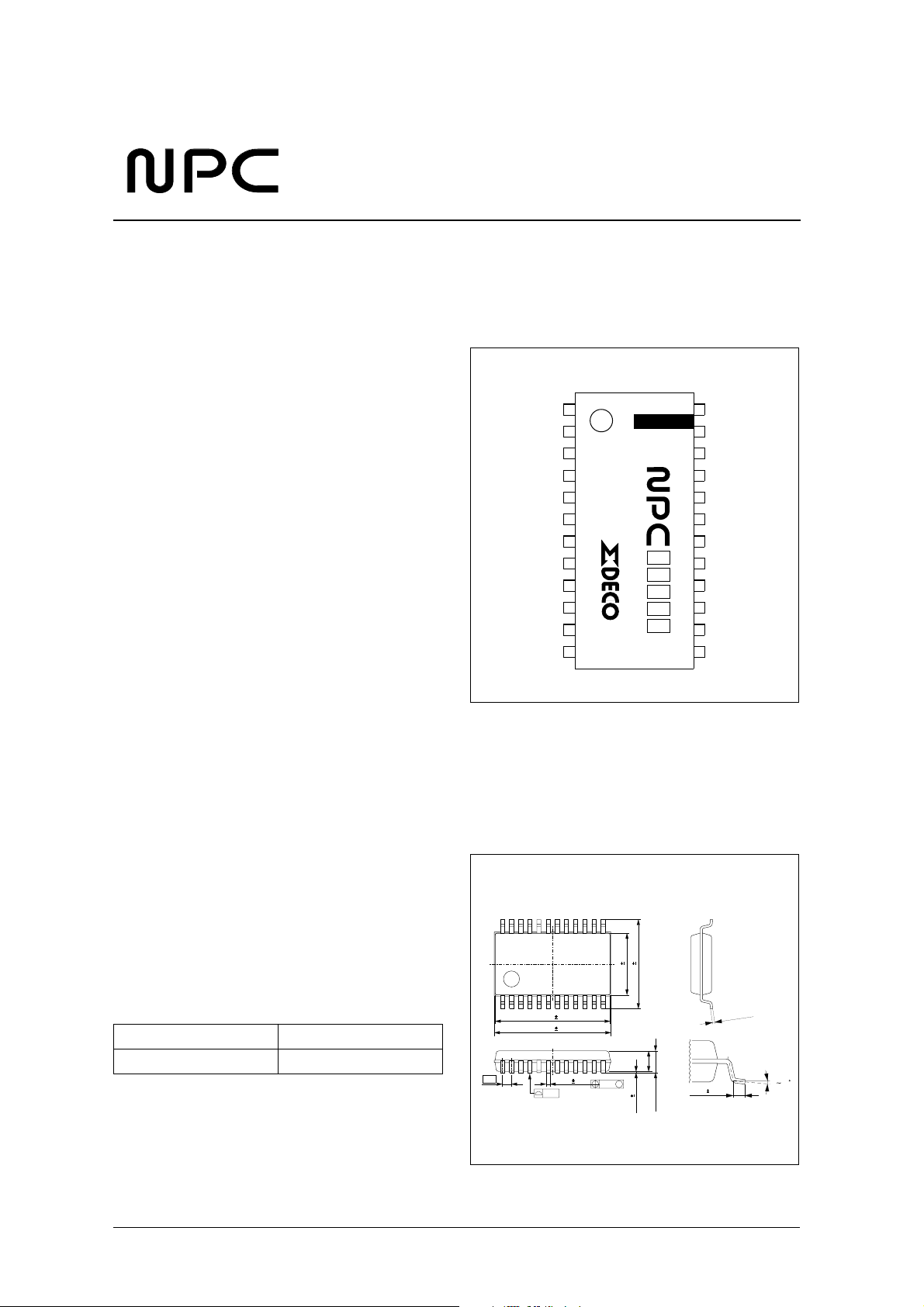
24-pin SSOP package
■
Molybdenum-gate CMOS process
ORDERING INFORMATION
Device Package
SM5865CM 24-pin SSOP
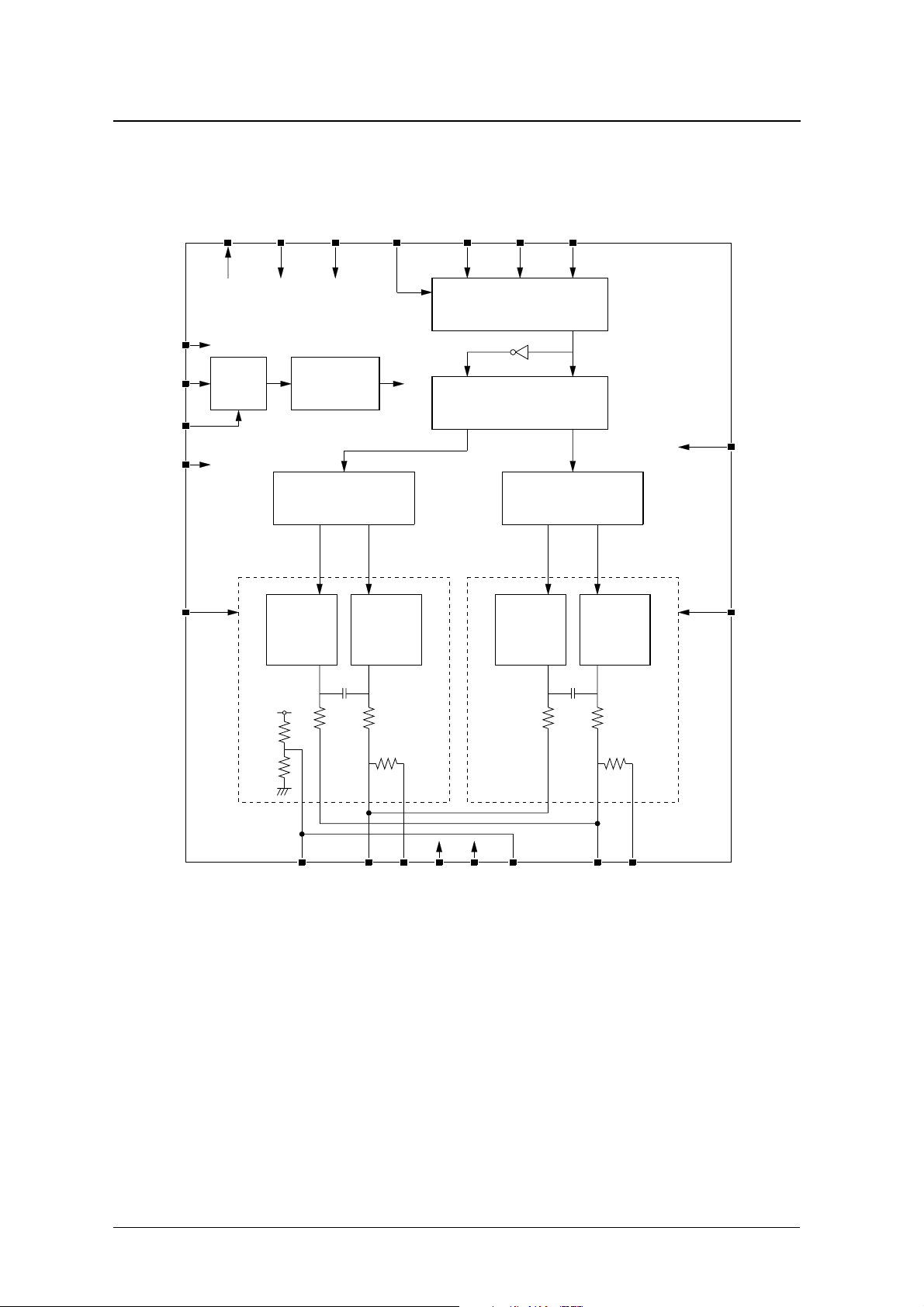
PACKAGE DIMENSIONS
(Unit: mm)
Weight: 0.23g
24-pin SSOP
7.80 0.30
5.40 0.20
10.05 0.20
10.20 0.30
0.8
0.10
0.36 0.10
0.12
M
1.80
+0.20
−0.10
1.90
0.10 0.10
0.50 0.20
0.15
0.10
+
0.05
−
010
NIPPON PRECISION CIRCUITS—1
BLOCK DIAGRAM
SM5865CM
DVDD
CKI
CKDVN
CVSS
AVSSB
TO TSTN
9
10
Divider
11
12
13
RSTN
Timing
control
Noise shaper
31 Level
DEM DAC
IWSL WCKI BCKI DI
Input interface
Interpolation
31 Level
DEM DAC
31 Level
DEM DAC
2345678
Noise shaper
31 Level
DEM DAC
1
DVSS
24
AVSSA
15 16 17 18 19 21 22 23
VBB
IOUTB
RB
AVDDB
AVDDA
VBA
IOUTA
NIPPON PRECISION CIRCUITS—2
RA
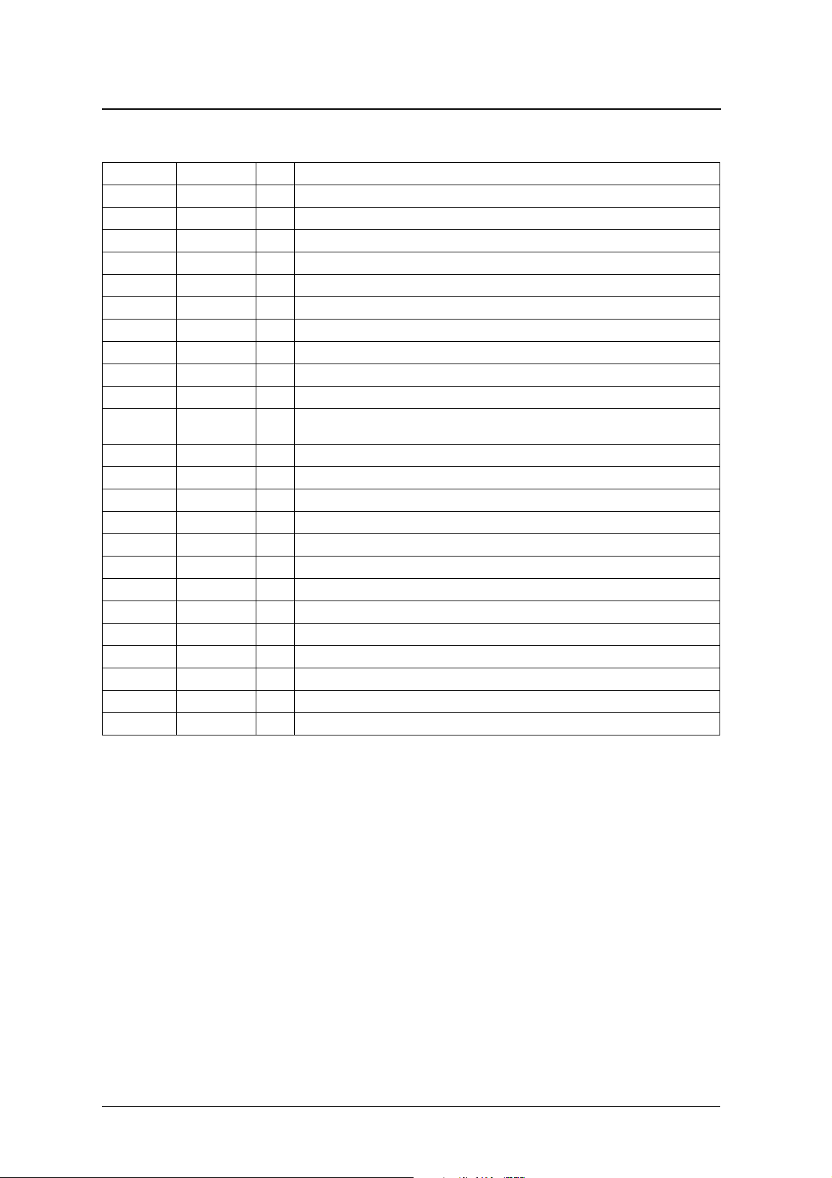
SM5865CM
PIN DESCRIPTION
Number Name I/O Description
1 DVSS – Digital ground
2 DI I Data input
3 BCKI I Bit clock input
4 WCKI I Word clock input
5 IWSL Ip Input data word length select. 24-bit when HIGH, and 20-bit when LOW.
6 RSTN Ip System reset. Reset when LOW.
7 TSTN Ip Test pin. Tie HIGH or leave open for normal operation.
8 TO O Test output
9 DVDD – Digital supply
10 CKI I System clock input
11 CKDVN Ip
12 CVSS – System clock ground
13 AVSSB – Analog ground B
14 N. C. – Leave open for no connection or connect with ground
15 VBB O 1/2 supply output B
16 IOUTB O Inverse-phase analog output B
17 RB I Built-in resistor connection B
18 AVDDB – Analog supply B
19 AVDDA – Analog supply A
20 N. C. – Leave open for no connection or connect with ground
21 VBA O 1/2 supply output A
22 IOUTA O In-phase analog output A
23 RA I Built-in resistor connection A
24 AVSSA – Analog ground A
System clock frequency divider ratio select. 1 when HIGH (no division), and 2 when LOW (half of the
input frequency).
I
: Pull-up input
P
NIPPON PRECISION CIRCUITS—3
−
−
°
−
°
SM5865CM
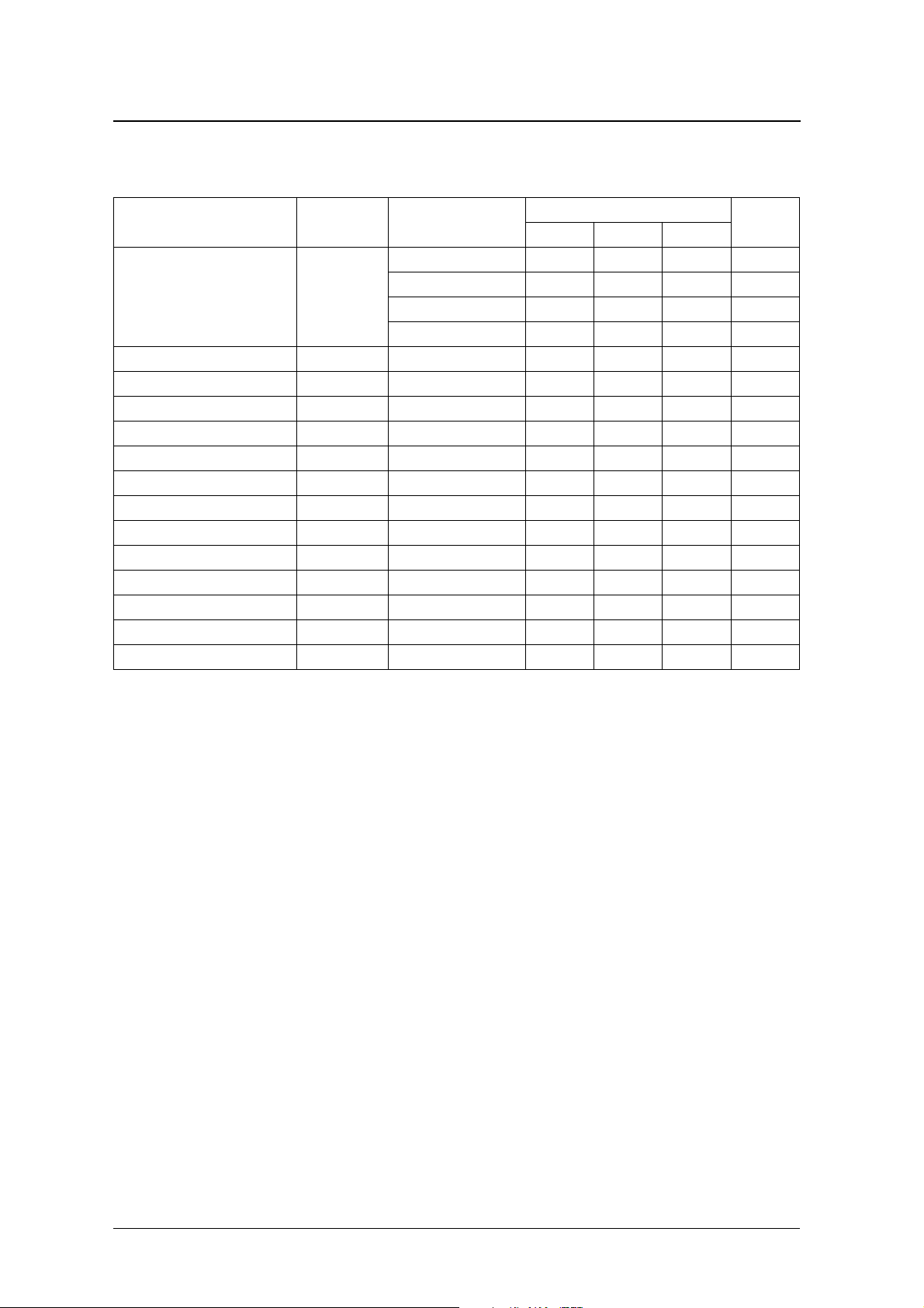
SPECIFICATIONS
Absolute Maximum Ratings
DVSS = AVSSA = AVSSB = CVSS = 0 V, DVDD = AVDDA = AVDDB
Parameter Symbol Rating Unit
Supply voltage range DVDD, AVDDA, AVDDB
Input voltage range
Storage temperature range T
Power dissipation P
1. Pins DI, BCKI, WCKI, CKDVN, IWSL, RSTN, TSTN.
Also applicable during supply switching.
Recommended Operating Conditions
DVSS = AVSSA = AVSSB = CVSS = 0 V, DVDD = AVDDA = AVDDB
1
V
IN
stg
D
0.3 to 7.0 V
DVSS − 0.3 to DVDD + 0.3 V
55 to 125
250 mW
C
Parameter Symbol Rating Unit
Supply voltage range DVDD, AVDDA, AVDDB 4.5 to 5.5 V
DVDD − AVDDA,
DVDD − AVDDB,
AVDDA − AVDDB,
Supply voltage variation
Operating temperature range T
DVSS − AVSSA,
DVSS − AVSSB,
AVSSA − AVSSB,
DVSS − CVSS,
AVSSA − CVSS,
AVSSB − CVSS
opr
±0.1 V
40 to 85
C
NIPPON PRECISION CIRCUITS—4
SM5865CM
DC Electrical Characteristics
Recommended operating conditions, unless otherwise specified.
Parameter Symbol Condition
DVDD, AVDDA, AVDDB
supply current
1
CKI HIGH-level input voltage V
CKI LOW-level input voltage V
CKI input voltage V
HIGH-level input voltage
LOW-level input voltage
HIGH-level output voltage
LOW-level output voltage
2
2
3
3
CKI HIGH-level input current I
CKI LOW-level input current I
LOW-level input current
HIGH-level input leakage current
LOW-level input leakage current
HIGH-level input leakage current
4
5
5
4
I
V
V
V
V
I
I
I
I
DD
IHC
ILC
INAC
IH
IL
OH
OL
IHC
ILC
IL2
IH1
IL1
IH2
1. No output load, NPC-standard input data pattern.
2. Pins DI, BCKI, WCKI, CKDVN, IWSL, RSTN, TSTN.
3. Pin TO.
4. Pins CKDVN, IWSL, RSTN, TSTN.
5. Pins DI, BCKI, WCKI.
Rating
Unit
min typ max
f
= 11.2896 MHz – 7 11 mA
CKI
f
= 16.9344 MHz – 10 14 mA
CKI
f
= 24.576 MHz – 15 19 mA
CKI
f
= 36.864 MHz – 21 26 mA
CKI
0.7 × DVDD – – V
– – 0.3 × DVDD V
AC coupling 1.0 – – Vp-p
2.4 – – V
– – 0.5 V
I
= − 1 mA DVDD − 0.4 – – V
OH
I
= 1 mA – – 0.4 V
OL
V
= DVDD 30 60 120 µA
IN
V
= 0 V 30 60 120 µA
IN
V
= 0 V – 5 15 µA
IN
V
= DVDD – – 1.0 µA
IN
V
= 0 V – – 1.0 µA
IN
V
= DVDD – – 1.0 µA
IN
NIPPON PRECISION CIRCUITS—5
AC Electrical Characteristics
System clock Input (CKI)
SM5865CM
Parameter Symbol
CKI clock frequency f
HIGH-level clock pulsewidth t
LOW-level clock pulsewidth t
CKI
t
CWL
Internal System Clock
Parameter Symbol Condition
Internal system clock frequency f
SYS
CKI
CWH
CWL
1/f
CKI
min typ max
5 – 60 MHz
5––ns
5––ns
t
CWH
min typ max
5 – 46 MHz
Rating
Rating
V
IHC
0.5∗DVDD
V
ILC
Unit
Unit
Internal system clock frequency is the same as the CKI clock frequency when CKDVN = HIGH.
Internal system clock frequency is half the CKI clock frequency when CKDVN = LOW.
Reset Input (RSTN)
Parameter Symbol Condition
RSTN LOW-level pulsewidth t
RSTN
At power ON 1 – – µs
After power ON 100 – – ns
Rating
min typ max
Unit
NIPPON PRECISION CIRCUITS—6

Serial input (BCKI, DI, WCKI)
SM5865CM
Parameter Symbol
BCKI HIGH-level pulsewidth t
BCKI LOW-level pulsewidth t
BCKI pulse cycle t
DI setup time t
DI hold time t
WCKI edge to first BCKI rising edge t
Last BCKI rising edge to WCKI edge t
BCKI
t
BCWH
t
BCY
BCWL
t
DI
t
DS
WCKI
BCWH
BCWL
BCY
DS
DH
WB
BW
t
DH
Rating
Unit
min typ max
10 – – ns
10 – – ns
22 – – ns
5––ns
5––ns
10 – – ns
10 – – ns
1.5V
1.5V
1.5V
t
WB
t
BW
Group Delay
Parameter Symbol Condition
min typ max
Group delay
1
T
gd
– – 2/fsi s
1. fsi is the input sampling rate of SM5865CM.
For example, fsi is 384kHz when this LSI is used in combination with an 8-times oversampling digital filter of which input sampling rate is 48kHz.
Rating
Unit
NIPPON PRECISION CIRCUITS—7

SM5865CM
AC Analog Characteristics
Measurement Conditions
External 8fs digital filter : NPC SM5847AF
External operational amplifier : JRC NJM5534D
Supply voltage SM5865CM : DVDD = AVDDA = AVDDB = 5V,
DVSS = AVSSA = AVSSB = CVSS = 0V
SM5847AF : + 3.3V
NJM5534D : ± 15V
Ambient temperature : 25 ° C
Input data of SM5847AF : 48kHz sampling (fs), 24-bit data
System clock : 24.576MHz (= 512fs), (64fs noise shaper operation)
Audio analyzer : Audio Precision System Two (RMS mode)
Measurement filter condition : THD + N 22HzHPF, 20kHzLPF (FLP-A20K)
: D.R 22HzHPF, 22kHzLPF, A-weight (FIL-AWT)
: S/N 22HzHPF, 22kHzLPF, A-weight (FIL-AWT)
Measurement circuits diagram : See next page.
Analog Characteristics
Parameter Symbol Condition
Output level
Total harmonic distortion THD + N 1 kHz, 0 dB –
Dynamic range D.R 1 kHz, − 60 dB 111 117 – dB
Signal-to-noise ratio S/N 1 kHz, 0/ −∞ dB 117 120 – dB
Gain drift G.D – 10 – ppm/ ° C
1. V
1
is the output level of the first I–V conversion stage.
out
V
out
1 kHz, 0 dB 1.28 1.33 1.38 Vrms
min typ max
Rating
0.00030
( − 110.5dB)
Unit
0.00060
( − 104.4dB)
%
NIPPON PRECISION CIRCUITS—8

Measurement circuit
SM5865CM
J1
OUT 2Vrms
R5
470
C5
4.7µ
GND
VCC
R3
C3
220p
R1
5
7
2
C1
330p
GND
24
23
AVSSA
DVSSDIBCKI
1
2
820
RA
620
6
3
22
IOUTA
3
5
7
VCC
U1
NJM5534D
18
4
VDD
21
20
VBA
WCKI
4
5
VEE
C7
+
C6
N.C.
IWSL
6
2
VCC
470µ
0.1µ
19
18
AVDDB
AVDDA
RSTN
TSTNTODVDD
6
7
U3
NJM5534D
18
4
3
C2
GND
17
RB
8
R2
5
7
330p
16
IOUTB
9
VEE
820
15
10
6
2
DD
V
VBB
CKI
R4
620
U2
3
R6
14
N.C.
CKDVN
11
C4
220p
NJM5534D
18
4
4.7kR74.7k
GND
13
AVSSB
IC1
CVSS
12
GND
VEE
GND
SM5865CM
GND
DI
BCKI
VDD
WCKI
GND
C8
0.1µ
+
C9
GND
100µ
CKI
NIPPON PRECISION CIRCUITS—9

SM5865CM
Dynamics Characteristics (under Measurement Conditions in page 8)
+0
-10
-20
-30
-40
-50
-60
-70
d
B
-80
r
-90
A
-100
-110
-120
-130
-140
-150
-160
2k 4k 6k 8k 10kHz12k 14k 16k 18k 20k
Figure 1. 0dB input FFT (1)
(1kHz notchfilter 32768point 8average)
+0
-10
-20
-30
-40
-50
-60
-70
d
B
-80
r
-90
A
-100
-110
-120
-130
-140
-150
-160
2k 4k 6k 8k 10kHz12k 14k 16k 18k 20k
Figure 3. –60dB input FFT (32768point 8average)
+0
-10
-20
-30
-40
-50
-60
-70
d
B
-80
r
-90
A
-100
-110
-120
-130
-140
-150
-160
10k 20k 30k 40k 50kHz60k 70k 80k 90k 100k
Figure 2. 0dB input FFT (2)
(1kHz notchfilter 32768point 8average)
-80
-82
-84
-86
-88
-90
-92
-94
-96
-98
d
-100
B
-102
-104
-106
-108
-110
-112
-114
-116
-118
-120
500200100502010 1k 2k 5k 10k 20k
Hz
Figure 4. THD + N vs. Frequency
1
0.5
0.2
0.1
0.05
0.02
0.01
%
0.005
0.002
0.001
0.0005
0.0002
0.0001
-60 -55 -50 -45 -40 -35 -30 -25 -20 -15 -10 -5 +0
dBFS
Figure 5. THD + N(%) vs. Amplitude
+0
-10
-20
-30
-40
-50
-60
d
B
r
-70
A
-80
-90
-100
-110
-120
-130
-140
-140 -130 -120 -110 -100 -90 -80 -70 -60 -50 -40 -30 -20 -10 +0
dBFS
Figure 7. Linearity
-70
-72.5
-75
-77.5
-80
-82.5
-85
-87.5
-90
d
-92.5
B
-95
r
-97.5
A
-100
-102.5
-105
-107.5
-110
-112.5
-115
-117.5
-120
-60 -50 -40 -30 -20 -10 +0-70-80-90-100-110-120
dBFS
Figure 6. THD + N (dB) vs. Amplitude
+1
+0.9
+0.8
+0.7
+0.6
+0.5
+0.4
+0.3
+0.2
d
+0.1
B
+0
r
-0.1
A
-0.2
-0.3
-0.4
-0.5
-0.6
-0.7
-0.8
-0.9
-1
10 20 50 100 200 500 1k 2k 5k 10k 20k
Hz
Figure 8. Evaluation Board Frequency Response
NIPPON PRECISION CIRCUITS—10

SM5865CM
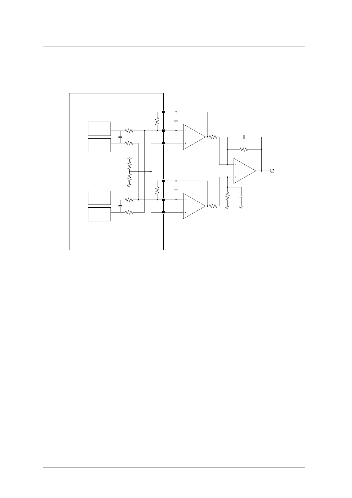
FUNCTIONAL DESCRIPTION
Analog Outputs
IOUTA, IOUTB
The SM5865CM input data in-phase signal is processed by noise shaper A and 31-level DEM-DAC with current output on differential output A, and input data reverse-phase signal is processed by noise shaper B and 31level DEM-DAC with current output on differential output B. Differential outputs A and B also have separate
in-phase and reverse-phase outputs: A in-phase output and B reverse-phase output are connected internally and
output on IOUTA, and B in-phase output and A reverse-phase output are connected internally and output on
IOUTB.
The IOUTA and IOUTB current outputs are I/V converted by external circuit and then input to a differential
input op-amp to obtain the final analog signal.
RA, RB
Internal resistors are connected between IOUTA and RA pins and between IOUTB and RB pins, which serve
as the op-amp feedback resistors. The feedback resistors have a resistance of 4.7kΩ.
The I/V converter output gain can be adjusted by connecting external resistors in parallel or serial with the
internal resistors. Note, however, that the internal resistance can vary from device to device by ±10%, and if
external resistors are used, the output level changes depending on the difference between each resistor ratio. If
the I/V converter gain is increased, a dynamic range higher even than that given in “Analog Characteristics
(page 8)” can be obtained.
Data input
Noise shaper A
Noise shaper B
Figure 9. Analog outputs
31 Level
DEM DAC
31 Level
DEM DAC
In-phase
output A
Inverse-phase
output A
In-phase
output B
Inverse-phase
output B
RA
IOUTA
RB
IOUTB
NIPPON PRECISION CIRCUITS—11
SM5865CM
VBA, VBB
A 0.5VDD signal is output from VBA, VBB using a resistor divider network. Using these pins allows the use
of the SM5865CM to replace the pin-compatible SM5865BM product.
RA
31 Level
DEM DAC
31 Level
DEM DAC
IOUTA
VBA
SM5865CM
RB
31 Level
DEM DAC
31 Level
DEM DAC
IOUTB
VBB
Figure 10. VBA, VBB
Audio Data Input (DI, BCKI, WCKI, IWSL)
■ Input data format
The audio data is input in MSB-first, 2s-complement, 24-bit/20-bit serial format. The input word bit length is
selected by IWSL, 24-bit when HIGH, and 20-bit when LOW.
■ Jitter-free function
The SM5865CM serial input data from DI synchronize with the word clock (WCKI) and are read into the first
register stage, and those also synchronize with the clock derived from divided system clock and are read into
the next register stage. This word clock and the system clock are always phase compared. When a phase shift
was detected, the comparison result is used to perform input timing adjustment in the system clock. Therefore
this process enable internal calculations not to be affected by generated large jitter on the word clock or changing the sampling rate during inputting data.
System Clock Divider (CKDVN)
The SM5865CM has a built-in clock frequency divider. The divider enables the internal system clock to operate at half the input frequency, for example when the external system clock input frequency is high.
System Reset (RSTN)
The device should be reset in the following cases.
■ At power ON
■ When the system clock CKI stops, or other abnormalities occur.
The device is reset by applying a LOW-level pulse on RSTN.
NIPPON PRECISION CIRCUITS—12

SM5865CM
Theoretical Quantization Noise Reduction
The SM5865CM employs a 3rd-order 31-level quantized noise shaper to widely reduce quantization noise in
the audio band to the high frequency bandwidth. The theoretical quantization noise level at 16fs to 96fs operation is shown in figure 11.
0
10
20
30
40
50
60
70
80
90
100
110
Quantization noise (dB)
120
130
140
150
160
170
180
0
0 dB sine wave equivalent white noise level
16-bit, fs quantization noise level
20-bit, fs quantization noise level
24-bit, fs quantization noise level
0.5 1 1.5 2 2.5 3 3.5 4
Frequency (fs)
16fs
24fs
32fs
48fs
64fs
96fs
Figure 11. Theoretical quantization noise level
NIPPON PRECISION CIRCUITS—13

SM5865CM
f
CKIfWCKI
16× n×=
f
nsfWCKI
n
f
CKI
16
-----------=×=
Internal Oversampling Operation
The SM5865CM accepts data output from an 8-times or 4-times oversampling digital filter, and oversampled
internally again up to the noise shaper operating rate. The internal oversampling factor is determined automatically from the system clock input frequency and the input sampling frequency. This internal oversampling factor (n) must be an integer satisfying the conditions shown in table 1.
Table 1. Operating conditions
Parameter CKDVN = HIGH CKDVN = LOW
f
and f
WCKI
Noise shaper operating frequency
1. f
WCKI
compulsory conditions
CKI
= word clock frequency, f
Word clock input
f
1
= input system clock frequency, n = internal oversampling factor
CKI
WCKI
CKIfWCKI
where n = 1, 2, 3, ... where n = 1, 2, 3, ...
f
nsfWCKI
SM5865CM
System clock input
8× n×=
f
CKI
-----------=×=
n
8
System clock divider select
CKI
Figure 12. Clock-related inputs
CKDVN
NIPPON PRECISION CIRCUITS—14

SM5865CM
System Clock Frequencies
Table 2 shows some possible combinations for the circuit configuration shown in figure 13.
fs
Interpolating filter
f
WCKI
SM5865CM
(8-times/4-times)
f
CKI
CKDVN
Figure 13. Circuit configuration
Table 2. System clock frequencies (CKDVN = HIGH)
1
fs
16 kHz 6.144 MHz (384fs) 48fs 6 12
16 kHz 8.192 MHz (512fs) 64fs 8 16
16 kHz 12.288 MHz (768fs) 96fs 12 24
32 kHz 6.144 MHz (192fs) 24fs 3 6
32 kHz 8.192 MHz (256fs) 32fs 4 8
32 kHz 12.288 MHz (384fs) 48fs 6 12
32 kHz 16.384 MHz (512fs) 64fs 8 16
32 kHz 24.576 MHz (768fs) 96fs 12 24
44.1 kHz 8.4672 MHz (192fs) 24fs 3 6
44.1 kHz 11.2896 MHz (256fs) 32fs 4 8
44.1 kHz 16.9344 MHz (384fs) 48fs 6 12
44.1 kHz 22.5792 MHz (512fs) 64fs 8 16
44.1 kHz 33.8688 MHz (768fs) 96fs 12 24
48 kHz 9.216 MHz (192fs) 24fs 3 6
48 kHz 12.288 MHz (256fs) 32fs 4 8
48 kHz 18.432 MHz (384fs) 48fs 6 12
48 kHz 24.576 MHz (512fs) 64fs 8 16
48 kHz 36.864 MHz (768fs) 96fs 12 24
88.2 kHz 16.9344 MHz (192fs) 24fs 3 6
88.2 kHz 22.5792 MHz (256fs) 32fs 4 8
88.2 kHz 33.8688 MHz (384fs) 48fs 6 12
88.2 kHz 45.1584 MHz (512fs) 64fs 8 16
96 kHz 18.432 MHz (192fs) 24fs 3 6
96 kHz 24.576 MHz (256fs) 32fs 4 8
96 kHz 36.864 MHz (384fs) 48fs 6 12
176.4 kHz 33.8688 MHz (192fs) 24fs 3 6
176.4 kHz 45.1584 MHz (256fs) 32fs 4 8
192 kHz 36.864 MHz (192fs) 24fs 3 6
1. When CKDVN = LOW, the system clock frequency f
and internal factors.
System clock frequency
f
CKI
Noise shaper operating
is halved, so the values shown are half the input frequency required for the same sampling rate
CKI
rate
Internal factor
(8fs input)
Internal factor
(4fs input)
NIPPON PRECISION CIRCUITS—15

TIMING DIAGRAMS
192fs System Clock Input Timing
WCKI
CKI
BCKI
(1)20bit *
DI
BCKI
(2)20bit
DI
BCKI
(3)24bit
DI
MSB
12345678910111213141516 17 18 19 20
MSB
12345678910111213141516 17 18 19 20
SM5865CM
1 / 8fs
LSB
MSB
1 2 3 4 5 6 7 8 9 10111213141516 17 18 19 20
LSB
LSB
21 22 23 24
384fs System Clock Input Timing
WCKI
CKI
BCKI
(1)20bit *
DI
BCKI
(2)20bit
DI
BCKI
(3)24bit
DI
MSB
1 2 3 4 5 6 7 8 9 10111213141516 17 18 19 20
MSB
1 2 3 4 5 6 7 8 9 10111213141516 17 18 19 20
1 / 8fs
LSB
MSB
1 2 3 4 5 6 7 8 9 10111213141516 17 18 19 20
21 22 23 24
LSB
LSB
*: Data can be input at any period within the word clock cycle.
NIPPON PRECISION CIRCUITS—16

256fs System Clock Input Timing
WCKI
CKI
BCKI
(1)20bit *
DI
BCKI
(2)20bit
DI
BCKI
(3)24bit *
DI
MSB
12345678910111213141516 17 18 19 20
MSB
12345678910111213141516 17 18 19 20
SM5865CM
1 / 8fs
LSB
MSB
1 2 3 4 5 6 7 8 9 10 11 12 13 14 15 16 17 18 19 20
LSB
21 22 23 24
LSB
BCKI
(4)24bit
DI
512fs System Clock Input Timing
WCKI
CKI
BCKI
(1)20bit *
DI
BCKI
(2)20bit
DI
BCKI
(3)24bit *
DI
MSB
12345678910111213141516 17 18 19 20
MSB
12345678910111213141516 17 18 19 20
MSB
1 2 3 4 5 6 7 8 9 10111213141516 17 18 19 20
1 / 8fs
LSB
MSB
1 2 3 4 5 6 7 8 9 10 11 12 13 14 15 16 17 18 19 20
LSB
21 22 23 24
LSB
21 22 23 24
LSB
BCKI
(4)24bit
DI
*: Data can be input at any period within the word clock cycle.
MSB
1 2 3 4 5 6 7 8 9 10111213141516 17 18 19 20
NIPPON PRECISION CIRCUITS—17
LSB
21 22 23 24

TYPICAL APPLICATIONS
Input Interface Circuit
SM5865CM
SM5847AF
XTI
WCKO
BCKO
DOL
DOR
CKI
DI
SM5865CM
WCKI
BCKI
CKI
DI
SM5865CM
WCKI
BCKI
NIPPON PRECISION CIRCUITS—18

Analog Output Circuits
Analog Output Circuit 1
31 Level
DEM DAC
31 Level
DEM DAC
SM5865CM
RA
IOUTA
SM5865CM
31 Level
DEM DAC
31 Level
DEM DAC
Analog Output Circuit 2
31 Level
DEM DAC
31 Level
DEM DAC
RB
IOUTB
RA
IOUTA
SM5865CM
RB
31 Level
DEM DAC
31 Level
DEM DAC
Note that the output analog characteristics and other specifications are not guaranteed for particular formats or application circuits.
Note that NPC has no responsibility for patents related to application circuits in these datasheets.
IOUTB
NIPPON PRECISION CIRCUITS—19

SM5865CM
NIPPON PRECISION CIRCUITS INC. reserves the right to make changes to the products described in this data sheet in order to
improve the design or performance and to supply the best possible products. Nippon Precision Circuits Inc. assumes no responsibility for
the use of any circuits shown in this data sheet, conveys no license under any patent or other rights, and makes no claim that the circuits
are free from patent infringement. Applications for any devices shown in this data sheet are for illustration only and Nippon Precision
Circuits Inc. makes no claim or warranty that such applications will be suitable for the use specified without further testing or modification.
The products described in this data sheet are not intended to use for the apparatus which influence human lives due to the failure or
malfunction of the products. Customers are requested to comply with applicable laws and regulations in effect now and hereinafter,
including compliance with export controls on the distribution or dissemination of the products. Customers shall not export, directly or
indirectly, any products without first obtaining required licenses and approvals from appropriate government agencies.
NIPPON PRECISION CIRCUITS INC.
4-3, Fukuzumi 2-chome
Koto-ku, Tokyo 135-8430, Japan
Telephone: +81-3-3642-6661
NIPPON PRECISION CIRCUITS INC.
Facsimile: +81-3-3642-6698
http://www.npc.co.jp/
Email: sales
@npc.co.jp
NC0019AE 2000.12
NIPPON PRECISION CIRCUITS—20
 Loading...