

Σ∆
SM5865AM
NIPPON PRECISION CIRCUITS INC.
OVERVIEW
The SM5865AM is a 24-bit input D/A converter for
high-quality digital audio equipment. It comprises
newly developed DEM (dynamic element matching)
circuits, 3rd-order Σ∆ noise shaper and 23-level
quantizer to control wide-band residual quantization
noise in the signal band, making it ideal for application with high-frequency sampling formats. Also, the
order of the required final-stage analog lowpass filter
can be reduced, compared to filters for available
devices, enhancing output tone quality. The output
stage employs complementary outputs for high-accuracy analog signals, with appropriate lowpass filtering of the output signal.
A single SM5865AM IC can be used in combination
with an 8-times oversampling digital filter for conversion for a single audio channel.
FEATURES
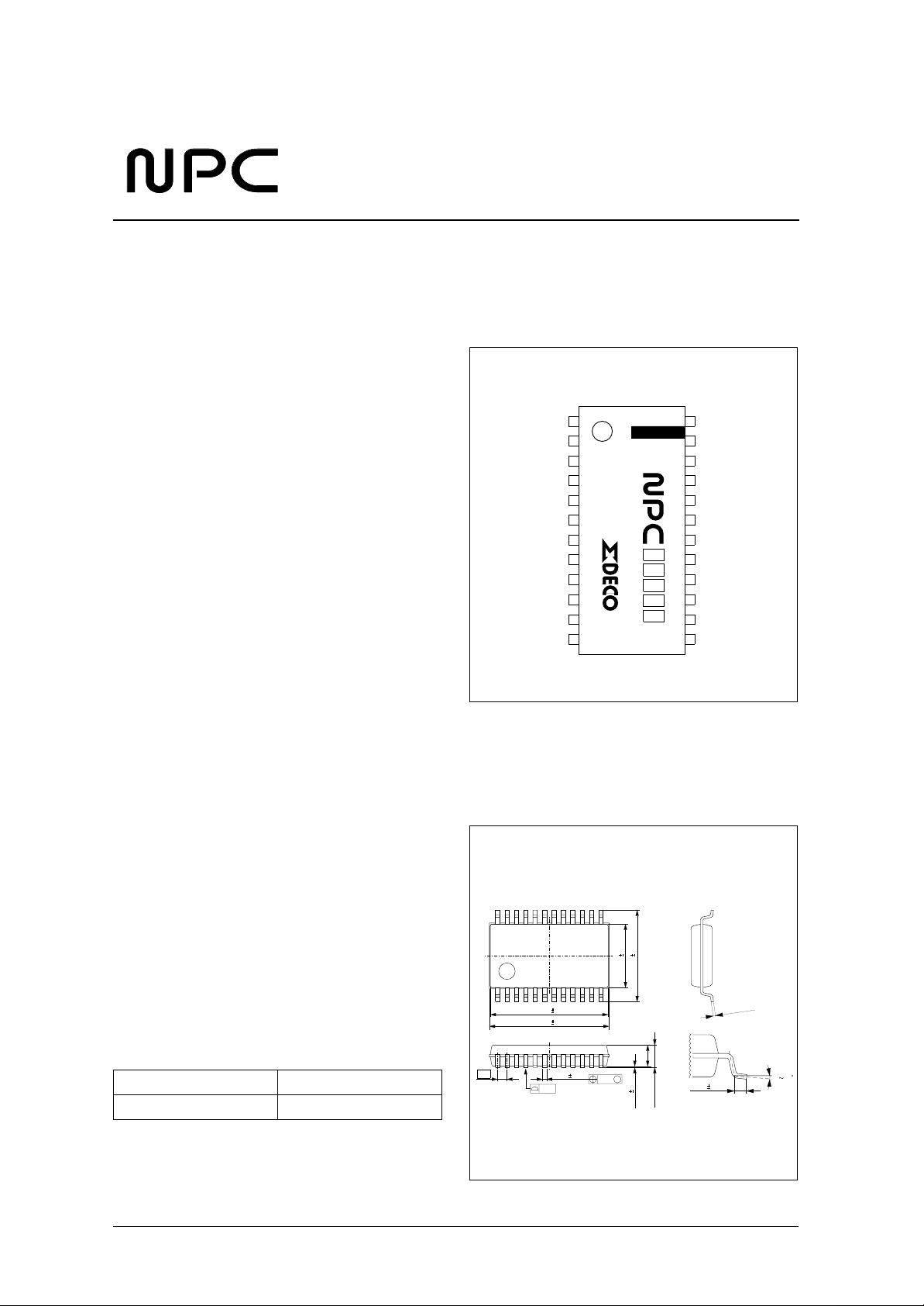
PINOUT
(Top view)
DVDD
CKDVN
DVSS
DI
BCKI
WCKI
IWSL
RSTN
TSTN
TO
CKI
CVSS
D/A Converter
1
SM5
865 M
A
12
24
13
AVSSA
RAP
IOUTA
IOUTAN
RAN
AVDDA
AVDDB
RBP
IOUTB
IOUTBN
RBN
AVSSB
Single-channel D/A converter built-in
■
High performance
■
(120 dB signal-to-noise ratio)
(0.001% total harmonic distortion and noise)
(110 dB dynamic range)
D/A converter
■
• 3rd-order noise shaper
• 23-level quantizer
Input data format
■
• 20 or 24-bit word length
• MSB first, right-justified format
• 8 or 4 times oversampling at fs = 32/44.1/48/
88.2/96/192 kHz
System clock frequency
■
• 128/192/256/384/512/768 fs
Single 5 V operating supply voltage
■
24-pin SSOP package
■
Molybdenum-gate CMOS process
■
ORDERING INFORMATION
Device Package
SM5865AM 24-pin SSOP
preliminary
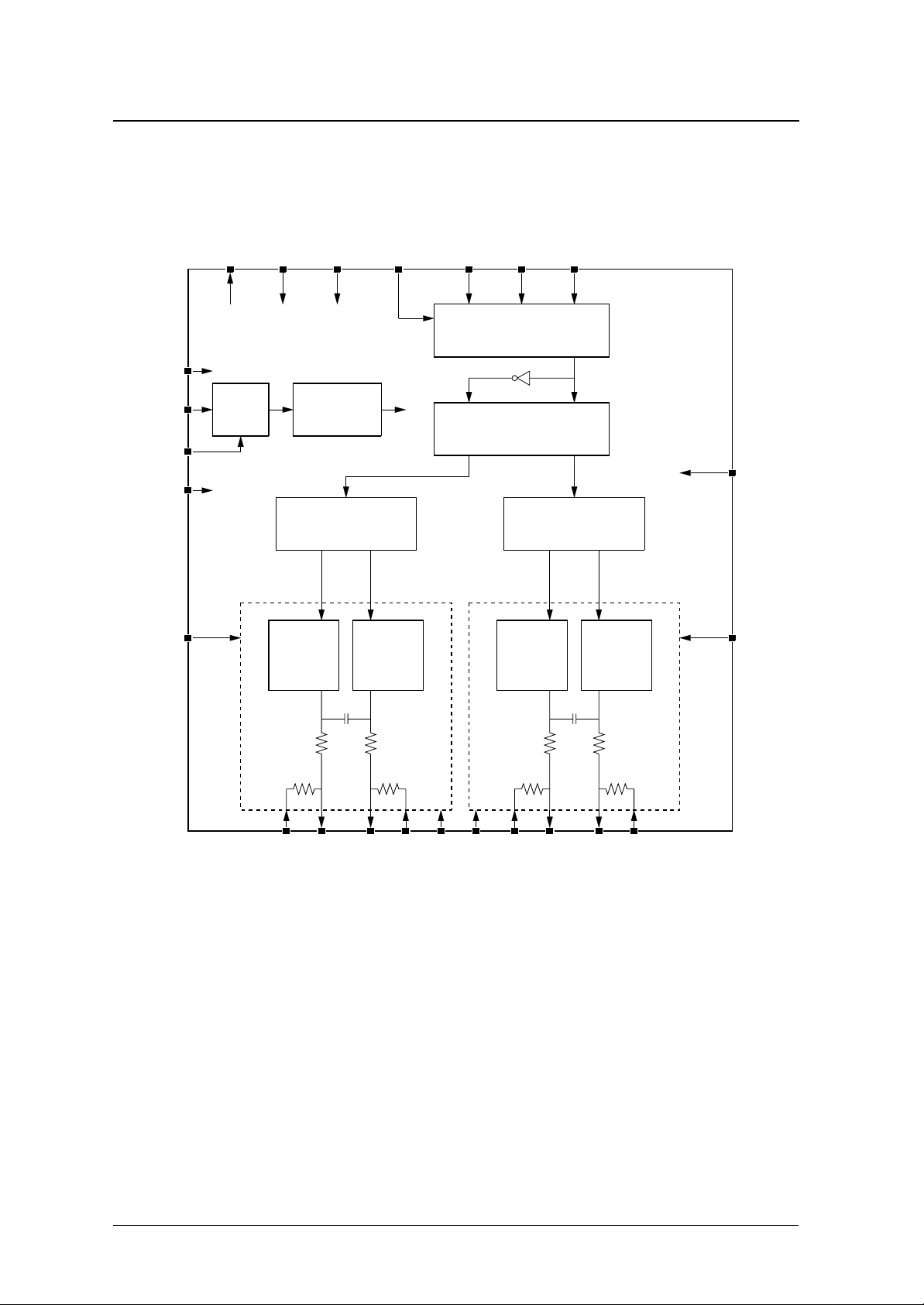
PACKAGE DIMENSIONS
(Unit: mm)
24-pin SSOP
7.80 0.30
5.40 0.20
10.05 0.20
10.20 0.30
0.8
0.10
0.36 0.10
0.12
M
1.80
+0.20
−0.10
1.90
0.10 0.10
0.50 0.20
0.15
0.1
+
0.05
−
010
NIPPON PRECISION CIRCUITS—1
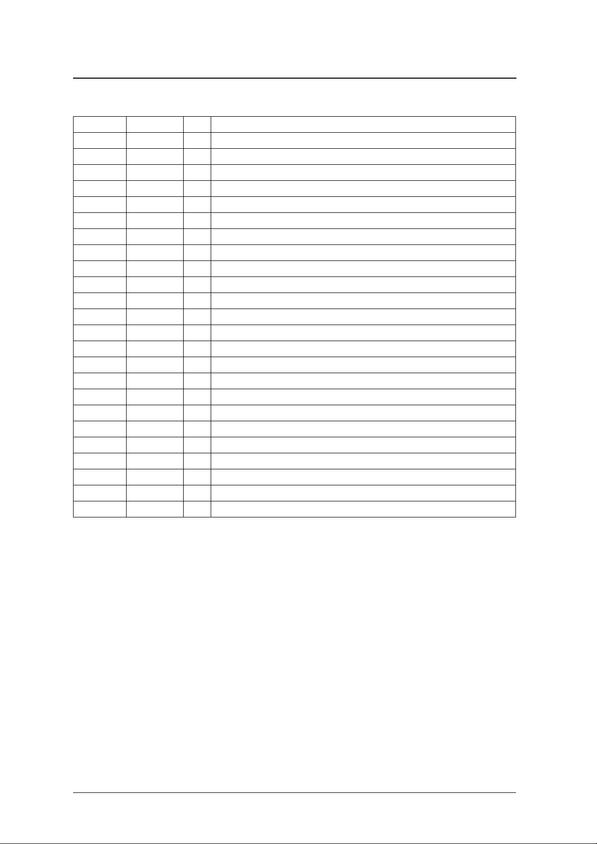
BLOCK DIAGRAM
SM5865AM
DVDD
CKI
CKDVN
CVSS
AVSSB
TO TSTN
9
10
Divider
11
12
13
RSTN
Timing
control
Noise shaper
23 Level
DEM DAC
IWSL WCKI BCKI DI
Input interface
Interpolation
23 Level
DEM DAC
23 Level
DEM DAC
2345678
Noise shaper
23 Level
DEM DAC
1
DVSS
24
AVSSA
14 15 16 17 18 19 20 21 22 23
RBN
IOUTBN
IOUTB
RBP
AVDDB
AVDDA
RAN
IOUTAN
IOUTA
RAP
preliminary
NIPPON PRECISION CIRCUITS—2
SM5865AM
PIN DESCRIPTION
Number Name I/O Description
1 DVSS – Digital ground
2 DI I Data input
3 BCKI I Bit clock input
4 WCKI I Word clock input
5 IWSL Ip Input data word length select. 24-bit when HIGH, and 20-bit when LOW.
6 RSTN Ip System reset. Reset when LOW.
7 TSTN Ip Test pin. Tie HIGH or leave open for normal operation.
8 TO O Test output
9 DVDD – Digital supply
10 CKI I System clock input
11 CKDVN Ip System clock frequency divider ratio select. 1 when HIGH (no division), and 2 when LOW.
12 CVSS – System clock ground
13 AVSSB – Analog ground B
14 RBN I Built-in resistor connection B
15 IOUTBN O Inverse-phase analog output B
16 IOUTB O In-phase analog output B
17 RBP I Built-in resistor connection B
18 AVDDB – Analog supply B
19 AVDDA – Analog supply A
20 RAN I Built-in resistor connection A
21 IOUTAN O Inverse-phase analog output A
22 IOUTA O In-phase analog output A
23 RAP I Built-in resistor connection A
24 AVSSA – Analog ground A
I
: Pull-up input
P
preliminary
NIPPON PRECISION CIRCUITS—3
−
−
+
−
°
°
SM5865AM
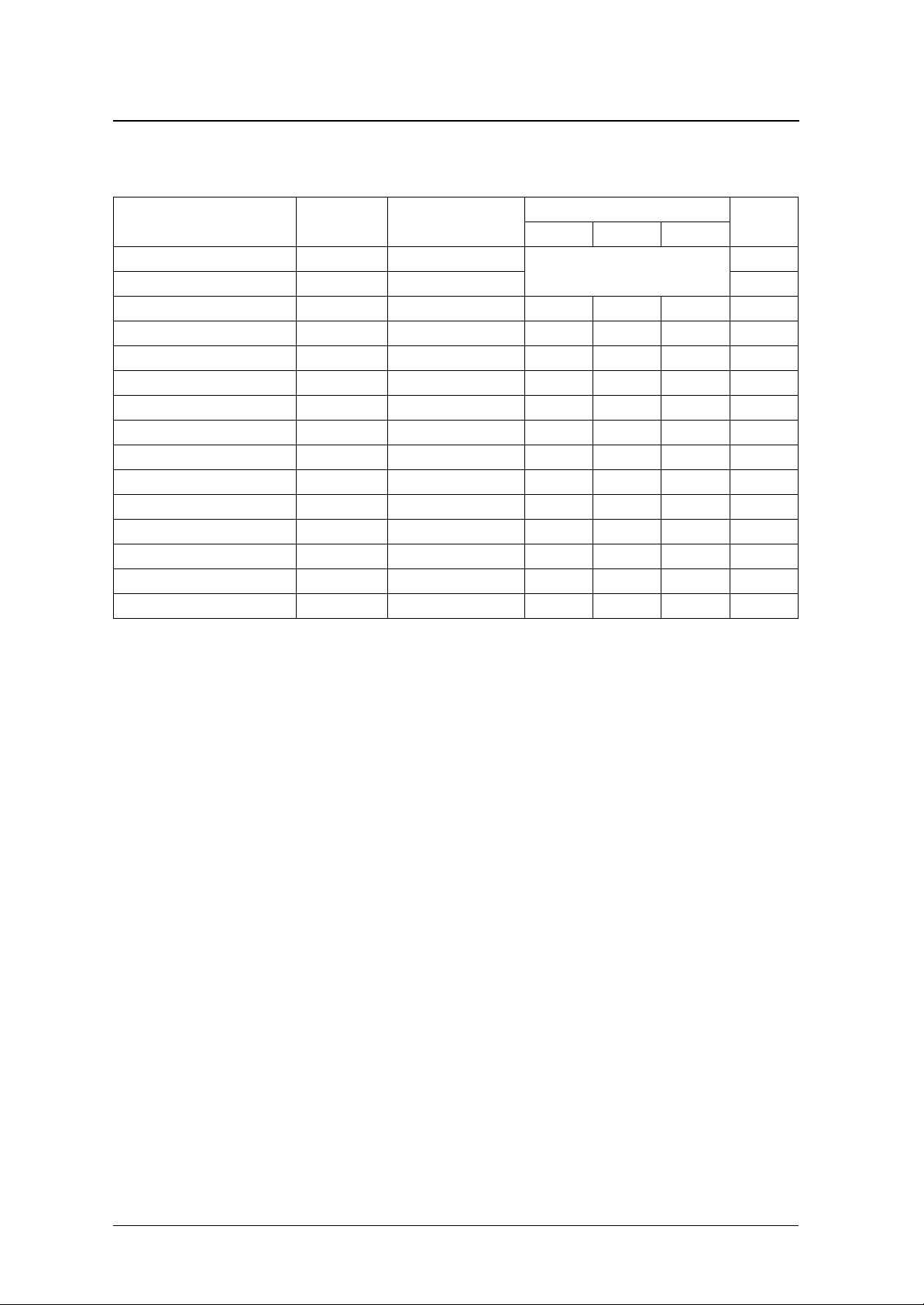
SPECIFICATIONS
Absolute Maximum Ratings
DV
= AV
SS
Supply voltage range DV
Input voltage range
Storage temperature range T
Power dissipation P
Soldering temperature T
Soldering time t
1. Pins DI, BCKI, WCKI, CKDVN, IWSL, RSTN, TSTN.
Also applicable during supply switching.
SSA
= AV
1
= CV
SSB
Parameter Symbol Rating Unit
= 0 V, DV
SS
DD
= AV
DD
DDA
, AV
V
DDA
IN
stg
sld
sld
D
−
−
= AV
, AV
−
DDB
−
DDB
−
−
−
−
−
−
°
0.3 to 7.0 V
DV
0.3 to DV
SS
55 to 125
250 mW
255
10 s
0.3 V
DD
C
C
Recommended Operating Conditions
DV
= AV
SS
Supply voltage range DV
Supply voltage variation
Operating temperature range T
SSA
= AV
= CV
SSB
Parameter Symbol Rating Unit
= 0 V, DV
SS
DD
= AV
DD
DV
DV
AV
DV
DV
AV
DV
AV
AV
DDA
, AV
DD
DD
DDA
SS
SS
SSA
SS
SSA
SSB
DDA
AV
AV
AV
AV
AV
AV
CV
CV
CV
opr
= AV
, AV
DDB
DDA
DDB
DDB
,
SSA
,
SSB
SSB
,
SS
SS
SS
,
,
,
,
,
DDB
4.5 to 5.5 V
±0.1 V
40 to 85
C
preliminary
NIPPON PRECISION CIRCUITS—4
SM5865AM
DC Electrical Characteristics
Recommended operating conditions, unless otherwise specified
−
Parameter Symbol Condition
DDA
1
1
2
2
3
3
4
5
5
6
= AV
= 5 V, system clock input frequency f
DDB
I
I
V
V
DDD
DDA
IHC
ILC
INAC
V
V
OH
OL
IHC
ILC
I
IL2
I
IH1
I
IL1
I
IH2
IH
IL
DVDD supply current
AVDDA, AVDDB supply current
CKI HIGH-level input voltage V
CKI LOW-level input voltage V
CKI input voltage V
HIGH-level input voltage
LOW-level input voltage
HIGH-level output voltage
LOW-level output voltage
CKI HIGH-level input current I
CKI LOW-level input current I
LOW-level input current
HIGH-level input leakage current
LOW-level input leakage current
HIGH-level input leakage current
1. DV
= AV
DD
2. Pins DI, BCKI, WCKI, CKDVN, IWSL, RSTN, TSTN.
3. Pin TO.
4. Pins CKDVN, IWSL, RSTN, TSTN.
5. Pins DI, BCKI, WCKI.
6. Pins CKDVN, IWSL, RSTN, TSTN.
Rating
min typ max
Unit
TBD
0.7V
DD
– – 0.3V
AC coupling 1.0 – – V
2.4 – – V
– – 0.5 V
I
= − 1 mA DV
OH
I
= 1 mA – – 0.4 V
OL
V
= DV
IN
DD
V
= 0 V 30 60 120 µA
IN
V
= 0 V – 9 18 µA
IN
V
= DV
IN
DD
V
= 0 V – – 1.0 µA
IN
V
= DV
IN
DD
= 16.9344 MHz, no output load, NPC-standard input data pattern.
CKI
0.4 – – V
DD
30 60 120 µA
– – 1.0 µA
– – 1.0 µA
––V
DD
mA
mA
V
preliminary
NIPPON PRECISION CIRCUITS—5
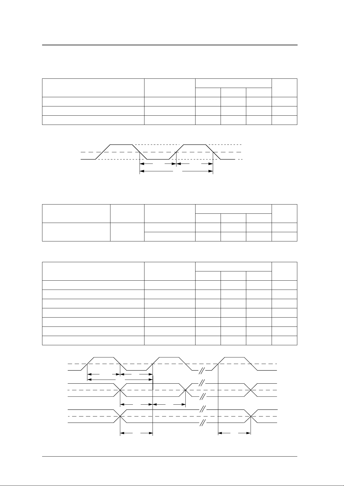
AC Electrical Characteristics
System clock (CKI)
SM5865AM
Parameter Symbol
HIGH-level clock pulsewidth t
LOW-level clock pulsewidth t
Clock pulse cycle t
CKI
t
CWL
Reset Input (RSTN)
Parameter Symbol Condition
RSTN LOW-level pulsewidth t
RSTN
At power ON 1 – – µs
After power ON 100 – – ns
CWH
CWL
CKI
Rating
min typ max
TBD – TBD ns
TBD – TBD ns
TBD – TBD ns
V
IH1
0.5V
DD
V
t
CWH
t
CKI
Rating
min typ max
IL1
Unit
Unit
Serial input (BCKI, DI, WCKI)
Parameter Symbol
BCKI HIGH-level pulsewidth t
BCKI LOW-level pulsewidth t
BCKI pulse cycle t
DI setup time t
DI hold time t
WCKI edge to first BCKI rising edge t
Last BCKI rising edge to WCKI edge t
BCKI
t
BCWH
t
BCY
BCWL
t
DI
t
preliminary
DS
WCKI
BCWH
BCWL
BCY
DS
DH
BW
WB
t
DH
Rating
Unit
min typ max
10 – – ns
10 – – ns
20 – – ns
5––ns
5––ns
10 – – ns
10 – – ns
1.5V
1.5V
1.5V
t
WB
t
WL
NIPPON PRECISION CIRCUITS—6

AC Analog Characteristics
SM5865AM
DVDD = AV
44.1 kHz input sampling frequency, f
Total harmonic distortion THD + N 1 kHz, 0 dB
LSI output level V
Dynamic range D.R 1 kHz, −60 dB dB
Signal-to-noise ratio S/N 1 kHz, 0/−∞ dB dB
Estimated values for audio signal data with up to 20 kHz bandwidth,
DVDD = AV
48 kHz input sampling frequency, f
96 kHz input sampling frequency, f
Total harmonic distortion THD + N 1 kHz, 0 dB
LSI output level V
Dynamic range D.R 1 kHz, −60 dB dB
Signal-to-noise ratio S/N 1 kHz, 0/−∞ dB dB
= AV
DDA
Parameter Symbol Condition
= AV
DDA
Parameter Symbol Condition
= 5 V, DVSS = AV
DDB
= 5 V, DVSS = AV
DDB
= AV
SSA
= 16.9344 MHz (384fs), 48fs operation
CKI
out1
CKI
CKI
out1
1 kHz, 0 dB Vrms
SSA
= 24.576 MHz (512fs), 64fs operation
= 24.576 MHz (256fs), 32fs operation
1 kHz, 0 dB Vrms
= AV
SSB
SSB
= CVSS = 0 V, Ta = 25 °C,
Rating
min typ max
TBD
= CVSS = 0 V, Ta = 25 °C,
Rating
min typ max
TBD
Unit
%
Unit
%
Measurement circuit block diagram
CKO(384fs)
Signal
Generator
Measurement conditions
DVDD = AV
Total harmonic distortion THD + N
Output level V
Dynamic range D.R D-RANGE
Signal-to-noise ratio S/N THRU
DDA
Parameter Symbol
BCK
WCKI
DATA
fs= 44.1kHz
= AV
= 5 V, DVSS = AV
DDB
preliminary
Evaluation
Board
out
10kΩ Input Impedance
NF Corporation 3346A
SSA
= AV
= CVSS = 0 V, Ta = 25 °C
SSB
3346A left/right-channel selector
L/R Channel
switch
THRU
Selector
Distortion
Analyzer
RMS Measurement
Corresponds to
Shibasoku AD725C
AD725C distortion analyzer with
built-in filter
20 kHz lowpass filter ON
400 Hz highpass filter OFF
20 kHz lowpass filter ON
400 Hz highpass filter OFF
JIS A filter ON
NIPPON PRECISION CIRCUITS—7

Measurement circuit
SM5865AM
TBD
preliminary
NIPPON PRECISION CIRCUITS—8

SM5865AM
f
CKIfWCKI
16× n×=
f
nsfWCKI
n
f
CKI
16
---------- -=×=
FUNCTIONAL DESCRIPTION
Quantization Noise Reduction
The SM5865AM employs a 3rd-order 23-level quantizer noise shaper to effectively reduce quantization noise
in the audio band. The quantization noise component at 16fs to 96fs operation is shown in figure 1.
0
Quantization noise
(dB)
10
20
30
40
50
60
70
80
90
100
110
120
130
140
150
160
170
180
0
0 dB sine wave equivalent white noise level
16-bit, fs quantization noise level
20-bit, fs quantization noise level
24-bit, fs quantization noise level
0.5 1 1.5 2 2.5 3 3.5 4
Frequency (fs)
16fs
24fs
32fs
48fs
64fs
96fs
Figure 1. Quantization noise level
Internal Oversampling Operation
The SM5865AM accepts data output from an 8-times or 4-times oversampling digital filter, and oversampled
internally again up to the noise shaper operating rate. The internal oversampling factor is determined automatically from the system clock input frequency and the input sampling frequency. This internal oversampling factor (n) must be an integer satisfying the conditions shown in table 1.
Table 1. Operating conditions
Parameter CKDVN = HIGH CKDVN = LOW
f
and f
WCKI
Noise shaper operating frequency
1. f
WCKI
compulsory conditions
CKI
= word clock frequency, f
f
1
= input system clock frequency, n = internal oversampling factor
CKI
preliminary
CKIfWCKI
where n = 1, 2, 3, ... where n = 1, 2, 3, ...
f
nsfWCKI
8× n×=
f
CKI
---------- -=×=
n
8
NIPPON PRECISION CIRCUITS—9

Word clock input
WCKI
SM5865AM
SM5865
System clock input
CKI
Figure 2. Clock-related inputs
Table 2 shows some possible combinations for the circuit configuration shown in figure 3.
fs
Table 2. System clock frequencies (CKDVN = HIGH)
fs
32 kHz 4.096 MHz (128fs) 16fs 2 4
System clock frequency
Interpolating filter
(8-times/4-times)
Figure 3. Circuit configuration
1
f
CKI
Noise shaper operating
rate
System clock divider select
CKDVN
f
WCKI
SM5865
f
CKI
Internal factor
(8fs input)
CKDVN
Internal factor
(4fs input)
32 kHz 6.144 MHz (192fs) 24fs 3 6
32 kHz 8.192 MHz (256fs) 32fs 4 8
32 kHz 12.288 MHz (384fs) 48fs 6 12
32 kHz 16.384 MHz (512fs) 64fs 8 16
32 kHz 24.576 MHz (768fs) 96fs 12 24
44.1 kHz 5.6448 MHz (128fs) 16fs 2 4
44.1 kHz 8.4672 MHz (192fs) 24fs 3 6
44.1 kHz 11.2896 MHz (256fs) 32fs 4 8
44.1 kHz 16.9344 MHz (384fs) 48fs 6 12
44.1 kHz 22.5792 MHz (512fs) 64fs 8 16
44.1 kHz 33.8688 MHz (768fs) 96fs 12 24
48 kHz 6.144 MHz (128fs) 16fs 2 4
48 kHz 9.216 MHz (192fs) 24fs 3 6
48 kHz 12.288 MHz (256fs) 32fs 4 8
48 kHz 18.432 MHz (384fs) 48fs 6 12
48 kHz 24.576 MHz (512fs) 64fs 8 16
48 kHz 36.864 MHz (768fs) 96fs 12 24
preliminary
NIPPON PRECISION CIRCUITS—10

SM5865AM
Table 2. System clock frequencies (CKDVN = HIGH)
1
fs
88.2 kHz 11.2896 MHz (128fs) 16fs 2 4
88.2 kHz 16.9344 MHz (192fs) 24fs 3 6
88.2 kHz 22.5792 MHz (256fs) 32fs 4 8
88.2 kHz 33.8688 MHz (384fs) 48fs 6 12
96 kHz 12.288 MHz (128fs) 16fs 2 4
96 kHz 18.432 MHz (192fs) 24fs 3 6
96 kHz 24.576 MHz (256fs) 32fs 4 8
96 kHz 36.864 MHz (384fs) 48fs 6 12
192 kHz 24.576 MHz (128fs) 16fs 2 4
192 kHz 36.864 MHz (192fs) 24fs 3 6
System clock frequency
f
CKI
Noise shaper operating
rate
Internal factor
(8fs input)
Internal factor
(4fs input)
1. When CKDVN = LOW, the system clock frequency f
and internal factors.
System Clock Divider (CKDVN)
The SM5865AM has a built-in divide-by-2 system
clock frequency divider. The divider enables the
internal system clock to operate at half the input frequency, for example when the external master clock
input frequency is high.
System Reset (RSTN)
The device should be reset in the following cases.
■ At power ON
■ When the system clock CKI stops, or other abnor-
malities occur.
The device is reset by applying a LOW-level pulse
on RSTN.
is halved, so the values shown are half the input frequency required for the same sampling rate
CKI
Audio Data Input (DI, BCKI, WCKI, IWSL)
Input data format
The audio data is input in MSB-first, 2s-complement, 24-bit/20-bit serial format. The input word bit
length is selected by IWSL, 24-bit when HIGH or
open circuit, and 20-bit when LOW.
Jitter-free function
Serial input data bits on DI are read into an SIPO
register (serial-to-parallel converter register) on the
rising edge of the bit clock BCKI where the serial
data is converted into parallel data. The internal parallel data control timing is derived from the system
clock, and is not affected by any jitter on the input
data clocks (WCKI and BCKI). After a reset operation is released when RSTN goes HIGH, the internal
timing and the WCKI input timing are phase compared on the first and subsequent WCKI falling
edges and the comparison result is used to perform
timing adjustment to maintain the word boundary
relationship between the internal timing and the
WCKI clock.
preliminary
NIPPON PRECISION CIRCUITS—11

TIMING DIAGRAMS
384fs System Clock Input Timing
WCKI
CKI
BCKI
(1)20bit *
DI
MSB
12345678910111213141516 17 18 19 20
SM5865AM
1 / 8fs
LSB
(2)20bit
(3)24bit
BCKI
DI
BCKI
DI
MSB
1 2 3 4 5 6 7 8 9 10111213141516 17 18 19 20
MSB
12345678910111213141516 17 18 19 20
* Data can be input at any period within the word clock cycle.
LSB
LSB
21 2223 24
preliminary
NIPPON PRECISION CIRCUITS—12

256fs System Clock Input Timing
WCKI
CKI
BCKI
(1)20bit *
DI
BCKI
(2)20bit
DI
MSB
12345678910111213141516 17 18 19 20
SM5865AM
1 / 8fs
LSB
MSB
1234567891011121314151617 1819 20
LSB
(3)24bit *
(4)24bit
BCKI
LSB
21 22 23 24
LSB
21 22 23 24
DI
BCKI
DI
MSB
12345678910111213141516 17 18 19 20
MSB
1 2 3 4 5 6 7 8 9 10 11 12 13 14 15 16 17 18 19 20
* Data can be input at any period within the word clock cycle.
preliminary
NIPPON PRECISION CIRCUITS—13

TYPICAL APPLICATIONS
Input Interface Circuit
SM5865AM
SM5847
XTI
WCKO
BCKO
DOL
DOR
CKI
DI
SM5865
WCKI
BCKI
CKI
DI
SM5865
WCKI
BCKI
preliminary
NIPPON PRECISION CIRCUITS—14

Analog Output Circuit 1
23 Level
DEM DAC
23 Level
DEM DAC
SM5865
23 Level
DEM DAC
23 Level
DEM DAC
SM5865AM
RAP
IOUTA
IOUTAN
RAN
RBP
IOUTB
IOUTBN
Analog Output Circuit 2
23 Level
DEM DAC
23 Level
DEM DAC
SM5865
23 Level
DEM DAC
23 Level
DEM DAC
preliminary
RBN
RAP
IOUTA
IOUTAN
RAN
RBP
IOUTB
IOUTBN
RBN
NIPPON PRECISION CIRCUITS—15

Analog Output Circuit 3
23 Level
DEM DAC
23 Level
DEM DAC
SM5865
23 Level
DEM DAC
23 Level
DEM DAC
SM5865AM
RAP
IOUTA
IOUTAN
RAN
RBP
IOUTB
IOUTBN
Analog Output Circuit 4
23 Level
DEM DAC
23 Level
DEM DAC
SM5865
23 Level
DEM DAC
23 Level
DEM DAC
preliminary
RBN
RAP
IOUTA
IOUTAN
RAN
RBP
IOUTB
IOUTBN
RBN
Note that the analog output characteristics are not guaranteed for non-standard output circuit configurations.
NIPPON PRECISION CIRCUITS—16

SM5865AM
NIPPON PRECISION CIRCUITS INC. reserves the right to make changes to the products described in this data sheet in order to
improve the design or performance and to supply the best possible products. Nippon Precision Circuits Inc. assumes no responsibility for
the use of any circuits shown in this data sheet, conveys no license under any patent or other rights, and makes no claim that the circuits
are free from patent infringement. Applications for any devices shown in this data sheet are for illustration only and Nippon Precision
Circuits Inc. makes no claim or warr anty that such applications will be suitab le for the use specified without further testing or modification.
The products described in this data sheet are not intended to use for the apparatus which influence human lives due to the failure or
malfunction of the products. Customers are requested to comply with applicable laws and regulations in effect now and hereinafter,
including compliance with export controls on the distribution or dissemination of the products. Customers shall not expor t, directly or
indirectly, any products without first obtaining required licenses and approvals from appropriate government agencies.
preliminary
NIPPON PRECISION CIRCUITS INC.
4-3, Fukuzumi 2-chome
Koto-ku, Tokyo 135-8430, Japan
NIPPON PRECISION CIRCUITS INC.
Telephone: 03-3642-6661
Facsimile: 03-3642-6698
NC9804BE 1999.2
NIPPON PRECISION CIRCUITS—17
 Loading...