SM5852DS
NIPPON PRECISION CIRCUITS INC.
OVERVIEW
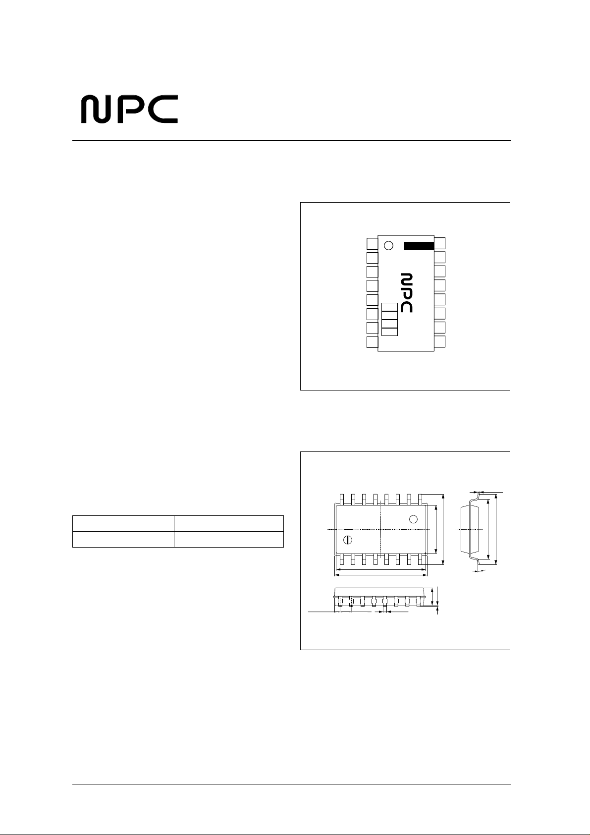
The SM5852DS is a digital signal processor IC that
performs XBS (extra bass system), LIVE (pseudosound field) and ASC (train position) processing for
use in digital audio reproduction equipment. It is
designed for use with a 44.1 kHz sampling
frequency.
FEATURES
■
2-channel processing
■
XBS/LIVE functions
■
XBS/LIVE processing bypass mode
■
ASC function ON/OFF switching
■
Input-level dependent dynamic gain characteristics
■
Serial input/output interface
2s complement, MSB first, 16-bit
■
384fs system clock
■
23 × 23-bit multiplier/30-bit high-precision
accumulator
■
TTL-compatible input/output
■
3.2 to 5.5 V operating voltage range
■
16-pin SOP
■
Molybdenum-gate CMOS
ORDERING INFOMATION
Digital Audio Processor LSI
PINOUT
LRCI
1
BCKI
2
DI
3
CLK
4
VSS
5
RSTN
6
TESTN
7
MUTEN
8
PACKAGE DIMENSIONS
16-pin SOP (Unit: mm)
SM5852DS
DB/DS
16
MOD2
15
MOD1
14
OPT
13
VDD
12
LRCO
11
BCKO
10
DOUT
9
0.17±0.05
Device Package
SM5852DS 16pin SOP
0.635±0.15
8.0±0.3
5.5±0.3
10.16±0.3
10.5 MAX
0.1±0.1
1.27±0.15
0.4±0.15
NIPPON PRECISION CIRCUITS—1
2.0±0.2
0 to 15
6.8±0.3
8.0±0.3

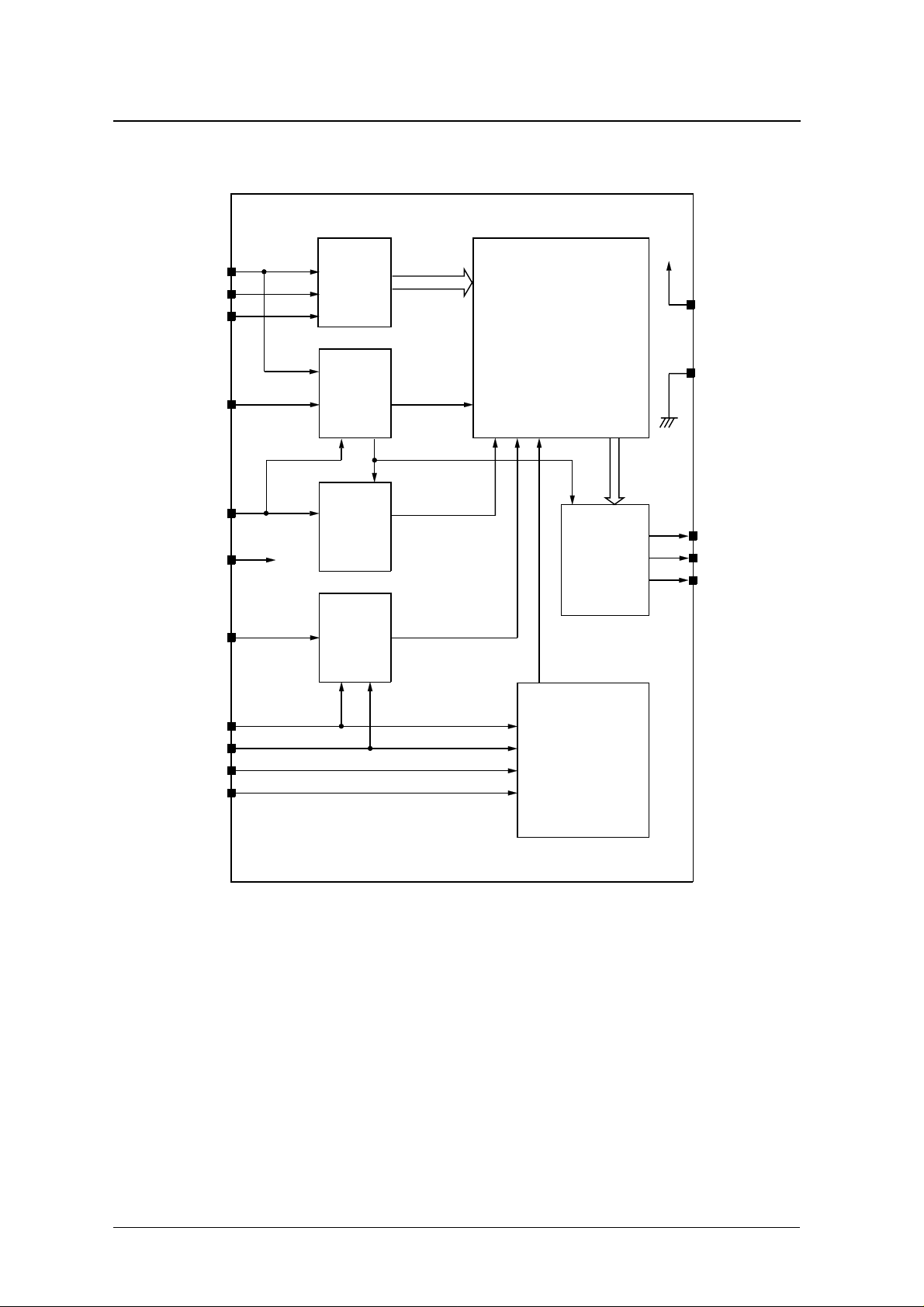
BLOCK DIAGRAM
SM5852DS
LRCI
BCKI
DI
CLK
RSTN
TESTN
MUTEN
Input data
Interface
System
Clock
Sequence
Control
Mute
Control
DSP Block
Output data
Interface
VDD
VSS
LRCO
BCKO
DOUT
DB/DS
OPT
MOD1
MOD2
Mode Control
NIPPON PRECISION CIRCUITS—2

PIN DESCRIPTION
SM5852DS
Number Name I/O
1 LRCI Ip Input data sample rate (fs) clock input
2 BCKI Ip Bit clock input
3 DI Ip Serial data input
4 CLK I Clock inpu t
5 VSS – Ground
6 RSTN Ip System reset initialization. Reset when LOW.
7 TESTN Ip Test mode input. Testing when LOW.
8 MUTEN Ip Mute input. Muting when LOW.
9 DOUT O Serial data output
10 BCKO O Bit clock output
11 LRCO O Output data sample rate (fs) clock output
12 VDD – 3.2 to 5.5 V supply
13 O P T Ip ASC ON/OFF switch control. OFF when HIGH, and ON when LOW.
14 MOD1 Ip
15 MOD2 Ip
16 DB/DS Ip
1. Ip = Input pin with pull-up resistor. Accordingly, they can be left open f or HIGH-level input.
1
XBS/LIVE low-pass gain select inputs. The XBS/LIVE function is bypassed when both MOD1
and MOD2 are HIGH.
LIVE ON/OFF switch control. OFF when HIGH, and ON when LOW. The LIVE function is
bypassed when both MOD1 and MOD2 are HIGH.
Description
NIPPON PRECISION CIRCUITS—3

−
−
−
°
°
−
° C
SPECIFICATIONS
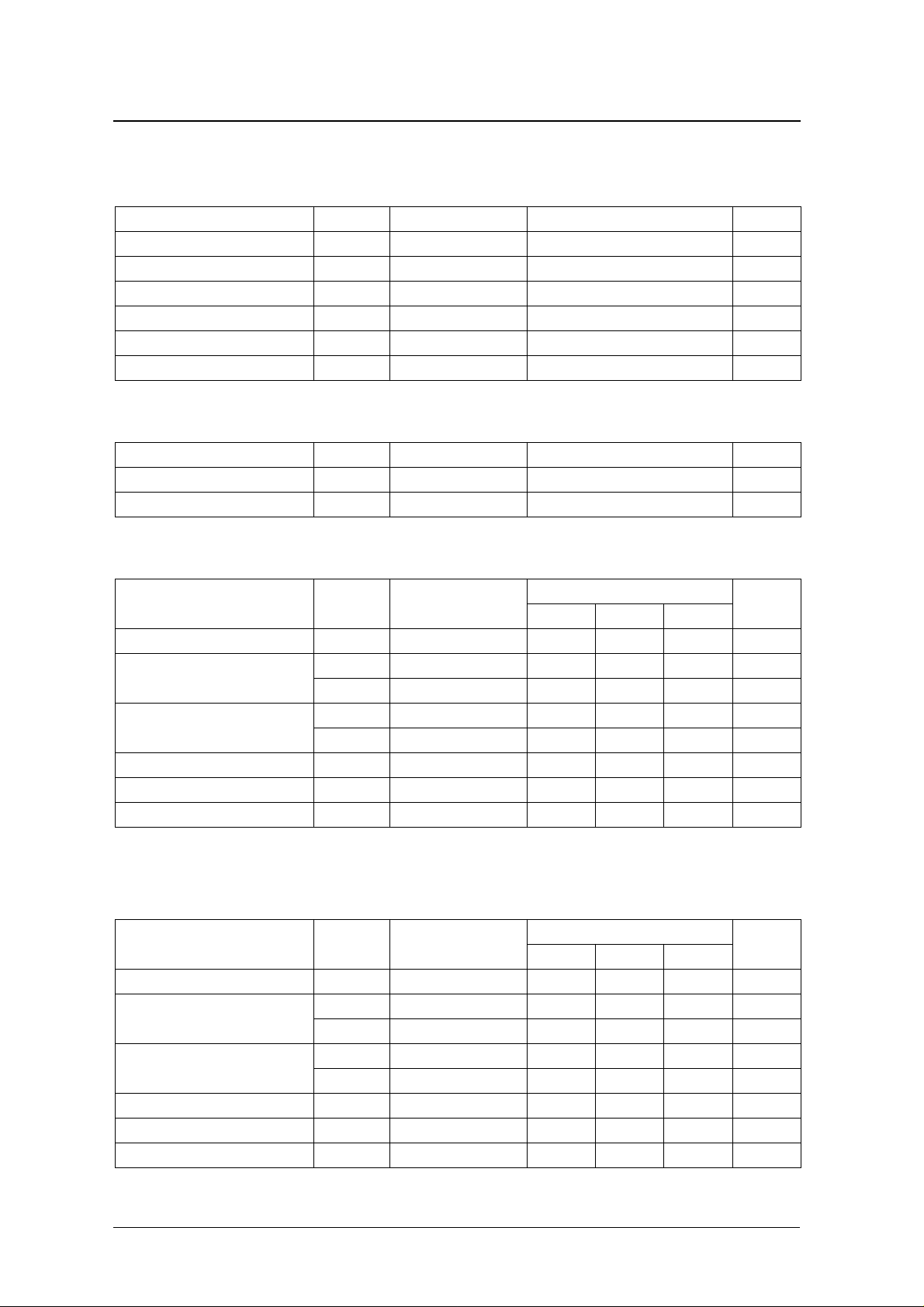
Absolute Maximum Ratings
V
= 0 V
SS
Parameter Symbol Condition Rating Unit
Supply voltage V
Input voltage V
Storage temperature T
Power dissipation P
Soldering temperature T
Soldering time t
Recommended Operating Conditions
V
= 0 V
SS
Parameter Symbol Condition Rating Unit
Supply voltage V
Operating temperature T
DD
IN
stg
D
sld
sld
DD
opr
SM5852DS
0.3 to 7.0 V
V
SS
0.3 to V
+ 0.3 V
DD
55 to 125
C
250 mW
255
C
10 s
3.2 to 5.5 V
20 to 80
DC Characteristics
Standard voltage: V
Parameter Symbol Condition
Current consumption
Input voltage for all inputs
Output voltage for all outputs
Input leakage current for all inputs
CLK input leakage current I
Input current for all inputs except CLK I
1. f
= 384fs = 16.9344 MHz, no output load, input data conformance with NPC test pattern
CLK
2. LRCI, BCKI, DI,RSTN, TESTN, MUTEN, OPT, MOD1, MOD2, DB / DS
3. LRCO, BCKO, DOUT
Low voltage: V
Parameter Symbol Condition
Current consumption
Input voltage for all inputs
Output voltage for all outputs
Input leakage current for all inputs I
CLK input leakage current I
Input current for all inputs except CLK I
1. f
= 384fs = 16.9344 MHz, no output load, input data conformance with NPC test pattern
CLK
2. LRCI, BCKI, DI,RSTN, TESTN, MUTEN, OPT, MOD1, MOD2, DB / DS
3. LRCO, BCKO, DOUT
= 4.5 to 5.5 V, V
DD
1
2
3
1
= 3.2 to 4.5 V, V
DD
1
2
3
SS
I
DD
V
IH
V
IL
V
OH
V
OL
I
LH
LL
IL
= 0 V, T
SS
I
DD
V
IH
V
IL
V
OH
V
OL
LH
LL
IL
= 0 V, T
= − 20 to 80 ° C
a
V
= 5.0 V – 16 23 mA
DD
I
= − 0.4 mA 2.5 – – V
OH
I
= 1.6 mA – – 0.4 V
OL
V
= V
IN
DD
V
= 0 V – – 1.0 µA
IN
V
= 0 V – – 20 µA
IN
= − 20 to 70 ° C
a
V
= 3.4 V – 7 10 mA
DD
I
= − 0.2 mA 2.5 – – V
OH
I
= 0.8 mA – – 0.4 V
OL
V
= V
IN
DD
V
= 0 V – – 1.0 µA
IN
V
= 0 V – – 12 µA
IN
Rating
Unit
min typ max
2.4 – – V
– – 0.5 V
– – 1.0 µA
Rating
Unit
min typ max
2.4 – – V
– – 0.5 V
– – 1.0 µA
NIPPON PRECISION CIRCUITS—4

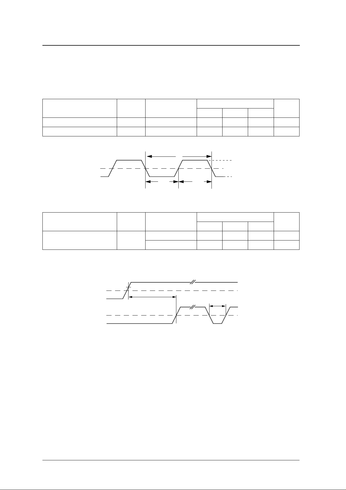
AC Characteristics
SM5852DS
Standard voltage: V
Low voltage: V
= 4.5 to 5.5 V, V
DD
= 3.2 to 4.5 V, V
DD
CLK (384fs)
Parameter Symbol Condition
Clock pulsewidth t
Clock cycle time t
CLK
RSTN
Parameter Symbol Condition
Reset LOW-level pulsewidth t
= 0 V, T
SS
CW
CY
RST
= 0 V, T
SS
= − 20 to 80 ° C
a
= − 20 to 70 ° C
a
tcy
Rating
min typ max
24 – 500 ns
55 59 1000 ns
VIH
1.5VDD
tCW
At power-ON 1 – – µs
At all other times 50 – 1000 ns
tCW
min typ max
VIL
Rating
Unit
Unit
3.2V
VDD
tRST 1µsec
RSTN
RSTN should be set LOW at power-ON and after
reacquiring synchronization. Note that if RSTN is
LOW for longer than 1 µs, a through-current flows in
the internal dynamic circuits because the internal
clock is stopped. The through-current has no rated
value, so the reset pulse should be kept as short as
possible at all times other than at power-ON.
tRST
1.5V
NIPPON PRECISION CIRCUITS—5
 Loading...