
SM5847AF
NIPPON PRECISION CIRCUITS INC.
High-fidelity Digital Audio, Multi-function Digital Filter
OVERVIEW
The SM5847AF is a 4/8-times oversampling (interpolation), 2-channel, linear-phase FIR, multi-function digital filter for digital audio reproduction
equipment. It features independent left and rightchannel digital deemphasis filters and soft muting
function.
The input/output interface supports input data in
16/18/20/24-bit words, and output data in
18/20/22/24-bit words in either 4-times or 8-times
oversampling selectable output mode.
FEATURES
■
Left/right-channel (2-channel processing)
■
4-times/8-times oversampling (interpolation)
• 8-times interpolation filter
- 3-stage linear-phase FIR configuration
1st stage (fs to 2fs): 169-tap
2nd stage (2fs to 4fs): 29-tap
3rd stage (4fs to 8fs): 17-tap
- ≤ ±0.00002 dB passband ripple (0 to
0.4535fs)
- ≥ 117 dB stopband attenuation (0.5465fs to
7.4535fs)
• 4-times interpolation filter
- 2-stage linear-phase FIR configuration
1st stage (fs to 2fs): 169-tap
2nd stage (2fs to 4fs): 29-tap
- ≤ ±0.00002 dB passband ripple (0 to
0.4535fs)
- ≥ 116 dB stopband attenuation (0.5465fs to
3.4535fs)
■
Digital deemphasis
• IIR filter configuration
• fs = 32kHz, 44.1kHz, 48kHz
• 2-channel independent ON/OFF control
■
26 × 24-bit parallel multiplier/32-bit accumulator
■
Overflow limiter
■
Soft muting
• 2-channel independent ON/OFF control
■
Input data format
The internal system clock operates at either 192fs or
256fs selectable speed (where fs is the audio sampling frequency). Plus, the divide-by 1, 2, or 4
counter settings means that external clocks of 768fs/
384fs/192fs (192fs input) and 1024fs/512fs/256fs
(256fs input) are supported.
The SM5847AF operates from a single 3 to 5 V supply, and is available in 44-pin QFP packages.
• 2s complement, MSB first
• 3 selectable formats
- LR alternating, 16/18/20/24-bit serial, rightjustified data
- LR alternating, 24-bit serial, left-justified
data
- LR simultaneous, 24-bit serial, left-justified
data
■
Output data format
• 2s complement, MSB first, LR simultaneous
• 18/20/22/24-bit serial
• BCKO burst (NPC format)
■
Dither round-off processing
• Dither round-off ON/OFF selectable
■
25-bit internal data word length
■
Internal system clock
• 192fs/256fs selectable
• Maximum operating frequency
192fs mode: 37 MHz max (5 V)
20.7 MHz max (3 V)
256fs mode: 27.6 MHz max (5 V)
25 MHz max (3 V)
■
Jitter-free function
• Jitter-free/Sync mode selectable
■
Crystal oscillator circuit built-in
■
3 to 5 V supply
■
44-pin plastic QFP
■
CMOS process
ORDERING INFORMATION
De vice Pack ag e
SM5847AF 44-pin QFP
NIPPON PRECISION CIRCUITS—1
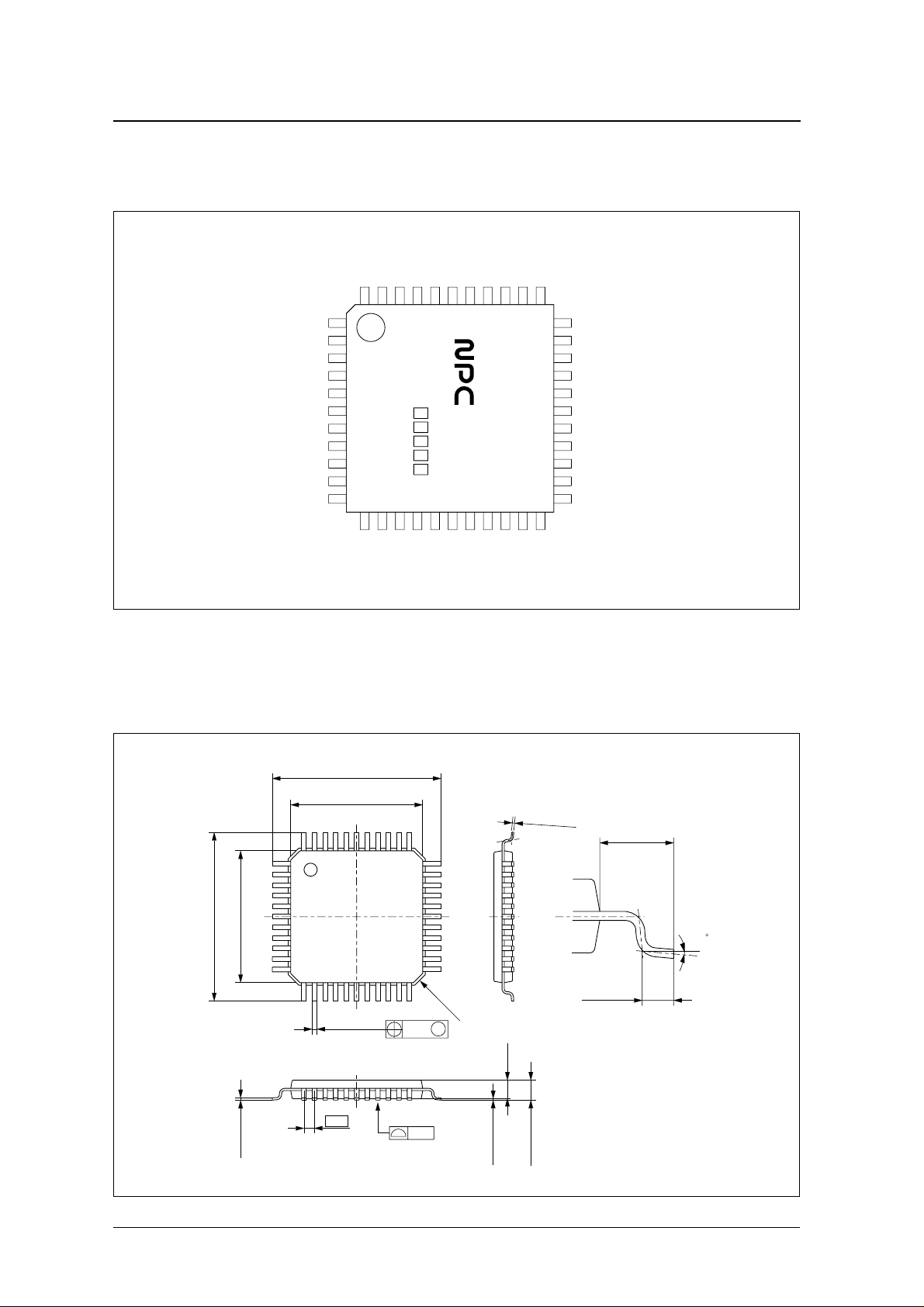
PINOUT
(T op V iew)
SM5847AF
OMD
DOR
DOL
WCKO
BCKO
VSS
VSSAC
VDDAC
VDD
DG
NC
PACKAGE DIMENSIONS
(Unit: mm)
44-pin plastic QFP
MUTEL
DITHN
MUTER
42
43
44
1
2
3
4
5
6
7
8
9
10
11
1213141516171819202122
VSS
CKO
VDD
FSEL2
41
SM58 4
7AF
XTO
FSEL1
40
XTI
VSS
39
VSS
VDD
38
VDD
DEMPL
DEMPR
36
37
LRCI
DI/INF2N
CKDV2
CKDV1
34
35
NC
BCKI
33
RSTN
32
SYNCN
31
OW2N
30
OW1N
29
VDD
28
VSS
27
IW2N/DIR
26
IW1N/DIL
25
INF1N
24
CKSLN
23
NC
0.30
+
−
12.80
+
10.00 0.30
+
0.17 0.05
+
12.80
0.30
−
+
10.00 0.30
−
0.17
+
0.05
−
(1.40)
−
0 to 10
0.35
4
−
C 0.7
+
0.10
−
0.20 M
0.60
+
0.20
−
(1.40)
−
0.80
0.15
+
−
0.15 0.05
0.20
+
−
1.50 0.10
NIPPON PRECISION CIRCUITS—2
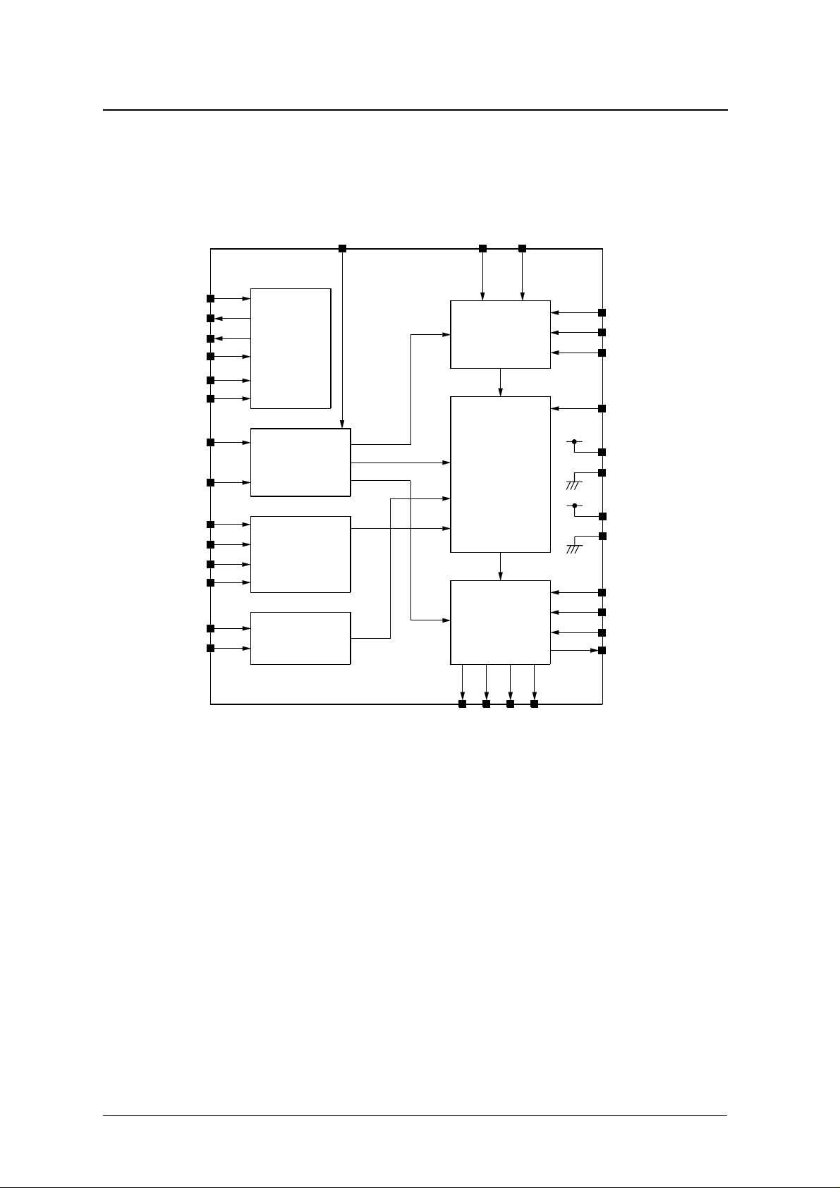
BLOCK DIAGRAM
SM5847AF
XTI
XTO
CKO
CKSLN
CKDV1
CKDV2
SYNCN
RSTN
DEMPL
DEMPR
FSEL1
FSEL2
MUTEL
MUTER
System
Clock
Timing
Controller
Deemphasis
Controller
Mute
Controller
LRCI
BCKI
Input Data
Interface
Filter and
Attenuation
Arithmetic
Block
Output Data
Interface
Block
DI/INF2N
IW1N/DIL
IW2N/DIR
INF1N
DITHN
VDD
VSS
VDDAC
VSSAC
OMD
OW1N
OW2N
DG
BCKO
DOL
WCKO
DOR
NIPPON PRECISION CIRCUITS—3
SM5847AF
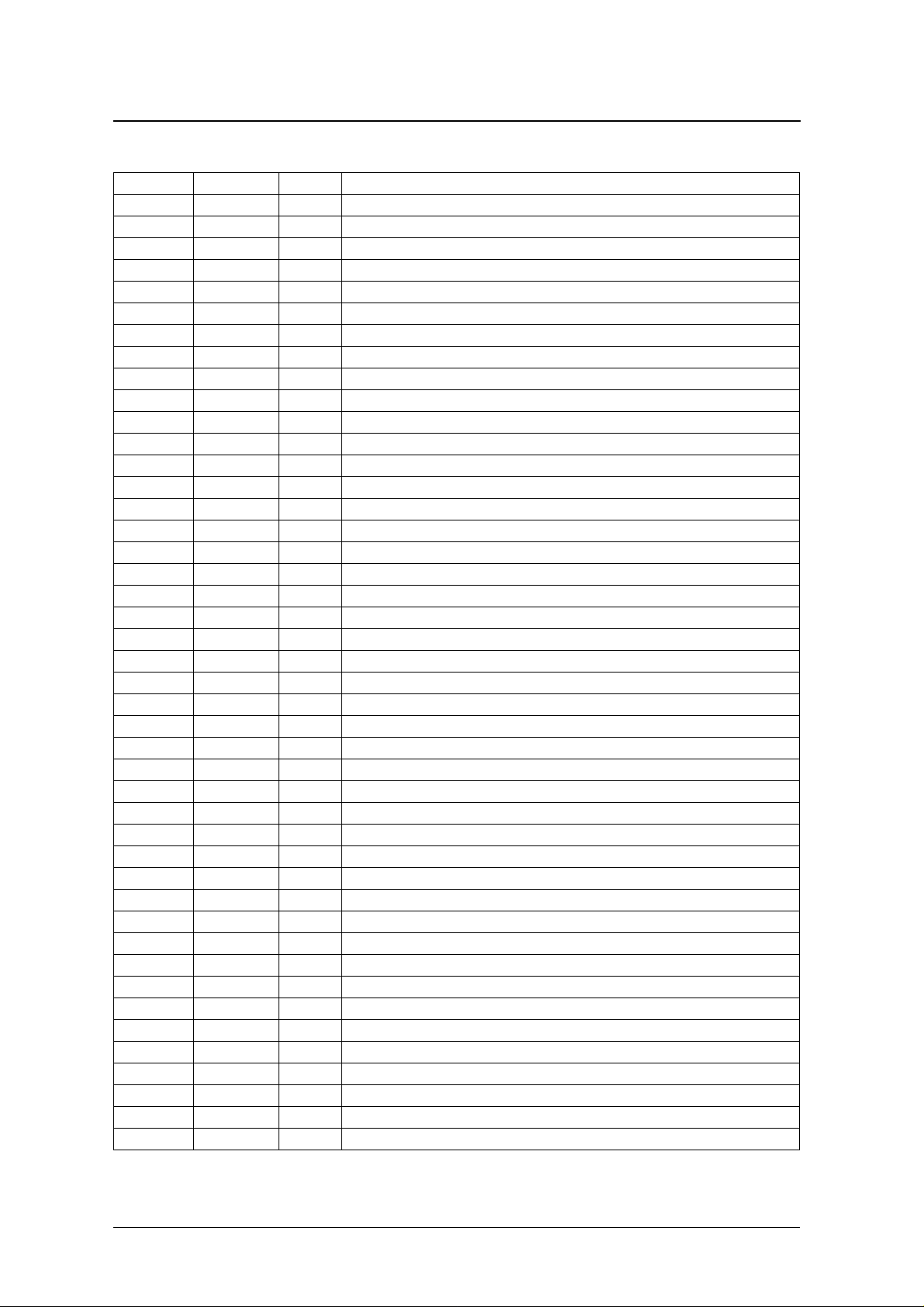
PIN DESCRIPTION
Number Name I/O Description
1
1 OMD Ip
2 DOR O
3 DOL O
4 WCKO O
5 BCKO O
6 VS S – Ground
7 VSSAC – Ground
8 V D D AC – Supply voltage
9 V D D – Supply voltage
10 D G O
11 N C – No internal connection (must be open)
12 CKO O
13 VS S – Ground
14 V D D – Supply voltage
15 X TO O Oscillator output
16 XTI I Oscillator input/master clock input
17 VS S – Ground
18 V D D – Supply voltage
19 LRCI I
20 DI/INF2N I
21 BCKI I
22 N C – No internal connection (must be open)
23 N C – No internal connection (must be open)
24 CKSLN Ip
25 INF1N Ip
26 IW1N/DIL Ip
27 IW2N/DIR Ip
28 VS S – Ground
29 V D D – Supply voltage
30 OW1N Ip
31 OW2N Ip
32 SYNCN Ip
33 RSTN Ip
34 CKDV1 Ip
35 CKDV2 Ip
36 DEMPR Ip
37 DEMPL Ip
38 V D D – Supply voltage
39 VS S – Ground
40 FSEL1 Ip
41 FSEL2 Ip
42 MUTEL Ip
43 MUTER Ip
44 DITHN Ip
1. Schmitt input, TTL level
2. TTL level
Ip = Pull-up input
Output data rate (4fs/8fs) select pin
2
Right-channel data output
2
Left-channel data output
2
Word clock output
2
Bit clock output
2
Deglitched signal output
2
Master clock output
1
Input data sample rate (fs) clock input
1
Data input/input format select pin 2
1
Bit clock input
2
Master clock frequency (192fs/256fs) select pin
2
Input format select pin 1
1
Input data word length select pin 1/left-channel data input
1
Input data word length select pin 2/right-channel data input
2
Output data word length select pin 1
2
Output data word length select pin 2
2
Sync mode select pin
1
Reset input
1
Internal system clock frequency divider set pin 1
1
Internal system clock frequency divider set pin 2
1
Right-channel deemphasis ON/OFF pin
1
Left-channel deemphasis ON/OFF pin
1
Deemphasis filter sample rate (fs) select pin 1
1
Deemphasis filter sample rate (fs) select pin 2
1
Left-channel mute ON/OFF pin
1
Right-channel mute ON/OFF pin
1
Output data dither ON/OFF pin
NIPPON PRECISION CIRCUITS—4
−
+
( °
−
−
°
≤
°
°
−
° C
−
−
−
−
−
−
−
SM5847AF
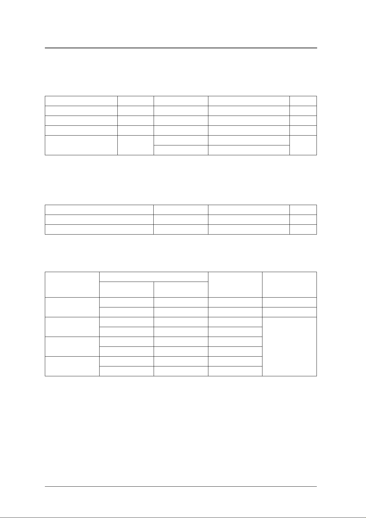
SPECIFICATIONS
Absolute Maximum Ratings
V
= V
SS
Supply voltage range
Input voltage range V
Storage temperature range T
Po w er dissipation P
1. Supply lines for VDD and VDD AC, and ground lines for VSS and VSSAC, should be connected on the printed circuit board to prevent device breakdo wn due to potential difference when the power is applied.
= 0 V, V
SSAC
Parameter Symbol Condition Rating Unit
1
DD
= V
DDAC
V
DD
, V
DDAC
I
stg
D
70
C 900
≤ 85
C 700
0.3 to 6.5 V
V
SS
0.3 to V
55 to 125
0.3 V
DD
C
mW
Recommended Operating Conditions
V
= V
SS
Supply voltage range
Operating temperature range T
1. The minimum required operating voltage and consequent operating temperature vary with the maximum operating frequency and sampling mode
selected, as shown in the following table.
V
= V
SS
Sampling frequency
1. Mode with internal frequency divider ratio set to 1 (CKDV1 = CK DV2 = L OW) .
2. 96 kHz + 12.5% variable pitch
3. 48 kHz + 15% variable pitch
SSAC
SSAC
fs (kHz)
192
2
108
96
3
55.2
= 0 V, V
1
= 0 V, V
= V
DD
DDAC
Parameter Symbol Rating Unit
V
DD
, V
DD
DDAC
a
= V
DDAC
Internal system clock
1
Mode
192fs 37 4.75 (5.0
256fs Not guaranteed Not guaranteed Not guaranteed
192fs 20.7 3.00 (3.3 −
256fs 27.6 4.50 (5.0
192fs 18.5 3.00 (3.3
256fs 25 3.00 (3.3
192fs 10.6 3.00 (3.3 −
256fs 14.2 3.00 (3.3
Maximum operating
frequency (MHz)
Minimum supply voltage
3.00 to 5.25 V
40 to 85
V
, V
DDAC
10%)
10%)
10%)
10%)
10%)
10%)
(V)
5%)
DD
Operating temperature
T
C)
a
40 to 70
40 to 85
NIPPON PRECISION CIRCUITS—5
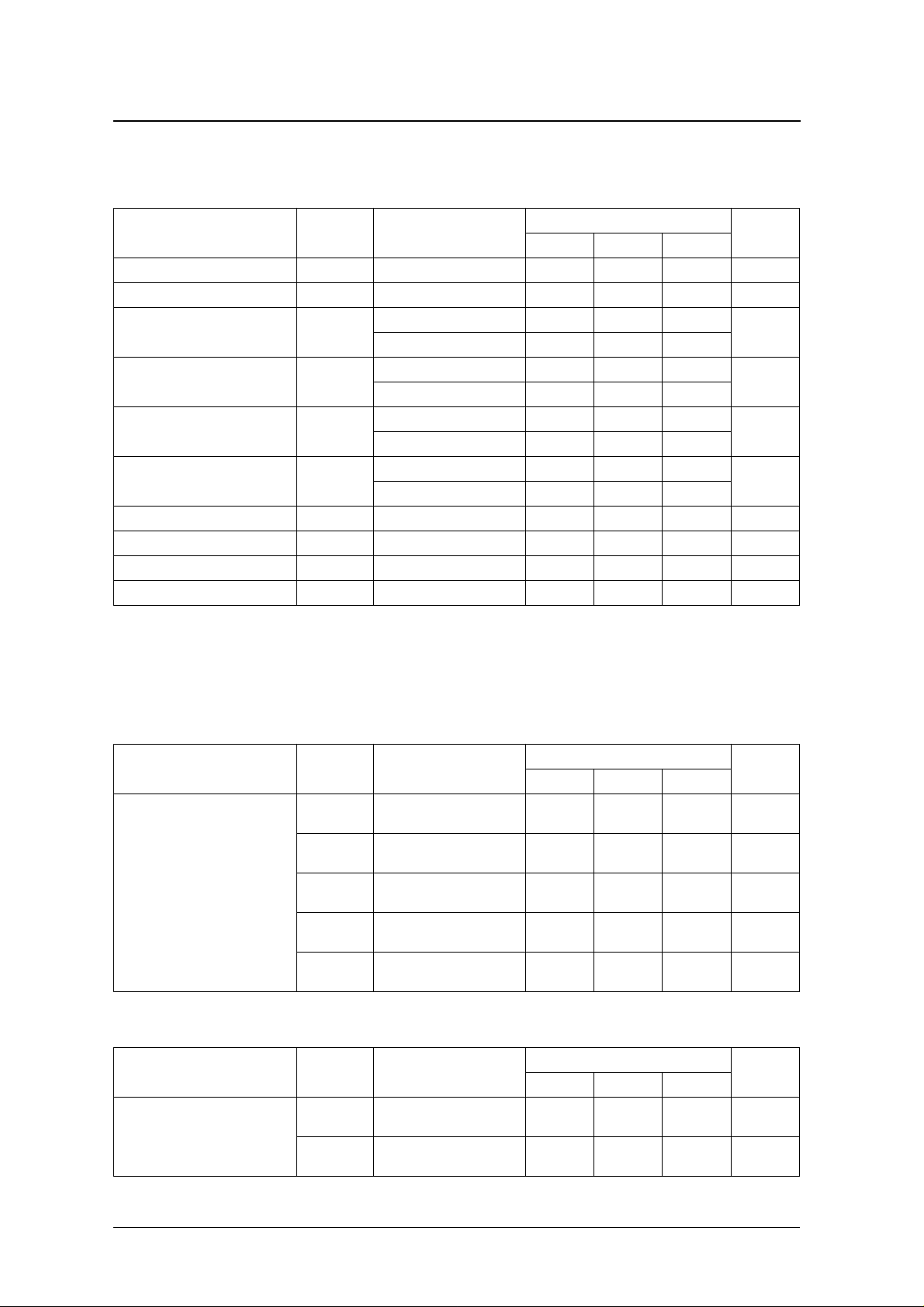
DC Electrical Characteristics
V
DD
= V
= 3.00 to 5.25 V, V
DDAC
SS
= V
SSAC
SM5847AF
= 0 V, T
= − 40 to 85 ° C
a
Parameter Symbol Condition
HIGH-level input voltage
HIGH-level input voltage
HIGH-level input voltage
L O W -level input voltage
L O W -level input voltage
L O W -level input voltage
Input leakage current
Input current
3,4
1
2,4
3
1
2,4
3
1,2
HIGH-level output voltage
L O W-level output voltage
min typ max
V
IH1
V
IH2
V
= V
V
IH3
V
IL1
DD
V
DD
V
DD
V
DD
VDD = V
V
IL2
VDD = V
VDD = V
V
IL3
I
IL1
I
IL2
5
5
V
OH
V
OL
VDD = V
VIN = 0 to 5.25 V
VIN = 0 V
IOH = −4 mA 2.4 – – V
IOL = 4 mA – – 0.4 V
= 4.75 to 5.25 V 2.4 – –
DDAC
= V
= 3.00 to 4.75 V 2.0 – –
DDAC
= V
= 4.75 to 5.25 V – – 0.3V
DDAC
= V
= 3.00 to 4.75 V – – 0.2V
DDAC
= 4.75 to 5.25 V – – 0.8
DDAC
= 3.00 to 4.75 V – – 0.2V
DDAC
= 4.75 to 5.25 V – – 0.8
DDAC
= 3.00 to 4.75 V – – 0.2V
DDAC
0.7V
DD
––V
2.0 – – V
DD
DD
DD
DD
−
10 – 10 µA
−
10
−
50
−
120 µA
Unit
V
V
V
V
1. Pin XTI
2. Pins LRCI, DI/INF2N, BCKI
3. Pins IW1N/DIL, IW2N/DIR
4. Pins OMD, CKSLN, INF1N, OW1N, OW2N, SYNCN, RSTN, CKDV1, CKDV2, DEMPR, DEMPL, FSEL1, FSEL2, MUTEL, MUTER, DITHN
5. Pins DOR, DOL, W C K O , BCKO, DG, CKO
Rating
V
DD
= V
= 4.75 to 5.25 V, V
DDAC
Parameter Symbol Condition
Current consumption
V
DD
= V
= 3.00 to 3.60 V, V
DDAC
Parameter Symbol Condition
Current consumption
SS
I
DD1
I
DD2
I
DD3
I
DD4
I
DD5
SS
I
DD6
I
DD7
= V
SSAC
= 0 V, T
192fs, XTI = 2 7 ns (37 MHz),
fs = 192 kHz,Ta = −40 to 70 °C
256fs, XTI = 4 0 ns (25 MHz),
fs = 9 6 kH z
384fs, XTI = 2 7 ns (37 MHz),
fs = 96 kHz, estimated value
192fs, XTI = 54 ns (18.5 MHz),
fs = 96 kHz, estimated value
384fs, XTI = 54 ns (18.5 MHz),
fs = 48 kHz, estimated value
= V
SSAC
= 0 V, T
256fs, XTI = 81 ns (12.3 MHz),
fs = 48 kHz, estimated value
384fs, XTI = 54 ns (18.5 MHz),
fs = 48 kHz, estimated value
= − 40 to 85 ° C, XTI = external input, no output load
a
Rating
Unit
min typ max
– – 166 m A
– – 115 m A
– – 105 m A
––95mA
––65mA
= − 40 to 85 ° C, XTI = external input, no output load
a
Rating
Unit
min typ max
––27mA
––28mA
NIPPON PRECISION CIRCUITS—6
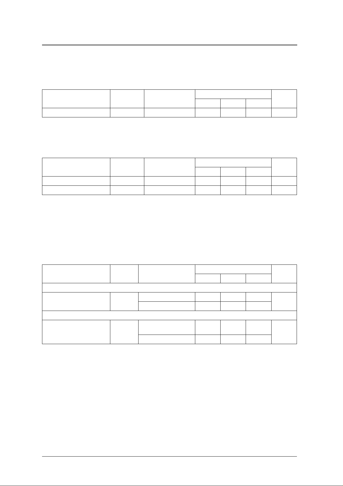
AC Electrical Characteristics
Crystal oscillator (XTI, XTO)
SM5847AF
VDD = V
Oscillator frequency
1. External circuit components should be matched for the crystal oscillator element used.
= 3.00 to 5.25 V, VSS = V
DDAC
Parameter Symbol Condition
1
f
OSC
= 0 V, Ta = −40 to 85 °C
SSAC
Rating
Unit
min typ max
– – 50 MHz
External clock input (XTI)
VDD = V
Master clock frequency f
Master clock duty 1/2VDD thresholds 40 – 60 %
= 3.00 to 5.25 V, VSS = V
DDAC
Parameter Symbol Condition
XTI
= 0 V, Ta = −40 to 85 °C
SSAC
Rating
Unit
min typ max
– – 60 MHz
Internal system clock
The crystal oscillator frequency or external clock input master clock frequency ratings are described in the preceding tables, but it is the internal system clock frequency rating, set by the internal frequency divider
(CKDV1, CKDV2), that must be satisfied. The master clock frequency is a multiple of the sampling frequency
fs.
CKDV1 = CKDV2 = LOW (internal system clock frequency = XTI input frequency),
VSS = V
256fs (CKSLN = LOW, CKDV1 = LOW, CKDV2 = LOW)
System clock frequency f
192fs (CKSLN = HIGH, CKDV1 = LOW , CKDV2 = LOW)
System clock frequency f
= 0 V, Ta = −40 to 85 °C
SSAC
Parameter Symbol Condition
SYS1
SYS2
VDD = V
VDD = V
VDD = V
Ta = −40 to 70 °C
VDD = V
= 4.50 to 5.25 V 0.256 – 27.6
DDAC
= 3.00 to 5.25 V 0.256 – 2 5
DDAC
= 4.75 to 5.25 V,
DDAC
= 3.00 to 5.25 V 0.384 – 20.7
DDAC
Rating
min typ max
0.384 – 3 7
Unit
MHz
MHz
NIPPON PRECISION CIRCUITS—7
SM5847AF
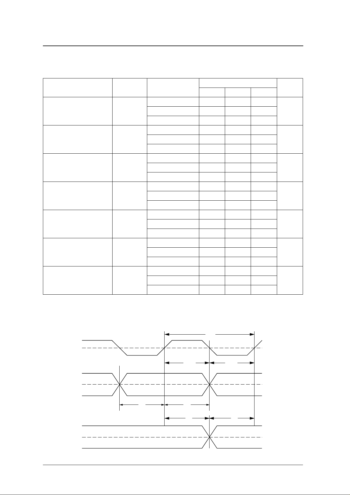
Serial input timing (BCKI, LRCI, DI/INF2N, IW1N/DIL, IW2N/DIR)
VSS = V
BCKI pulse cycle t
BCKI HIGH-level pulsewidth t
BCKI LOW-level pulsewidth t
DI, DIL, DIR setup time t
DI, DIL, DIR hold time t
Last BCKI rising edge to LRCI edge t
LRCI edge to first BCKI rising edge t
= 0 V, Ta = −40 to 85 °C
SSAC
Parameter Symbol Condition
IBCY
BCWH
BCWL
DS
DH
BL
LB
Rating
Unit
min typ max
Note 1 55 – –
nsNote 2 80 – –
Note 3 100 – –
Note 1 25 – –
nsNote 2 35 – –
Note 3 45 – –
Note 1 25 – –
nsNote 2 35 – –
Note 3 45 – –
Note 1 10 – –
nsNote 2 20 – –
Note 3 30 – –
Note 1 10 – –
nsNote 2 20 – –
Note 3 30 – –
Note 1 10 – –
nsNote 2 20 – –
Note 3 30 – –
Note 1 10 – –
nsNote 2 20 – –
Note 3 30 – –
1. CKSLN = HIGH (192fs), VDD = V
2. CKSLN = LOW (256fs), VDD = V
CKSLN = HIGH (192fs), VDD = V
3. CKSLN = LOW (256fs), V
DD
= V
BCKI
DI
DIL
DIR
LRCI
= 4.75 to 5.25 V, Ta = −40 to 70 °C
DDAC
= 4.50 to 5.25 V
DDAC
= 3.00 to 4.75 V
DDAC
= 3.00 to 4.50 V
DDAC
tDS
tIBCY
tBCWH tBCWL
tDH
tBL
NIPPON PRECISION CIRCUITS—8
1.5V
1.5V
tLB
1.5V
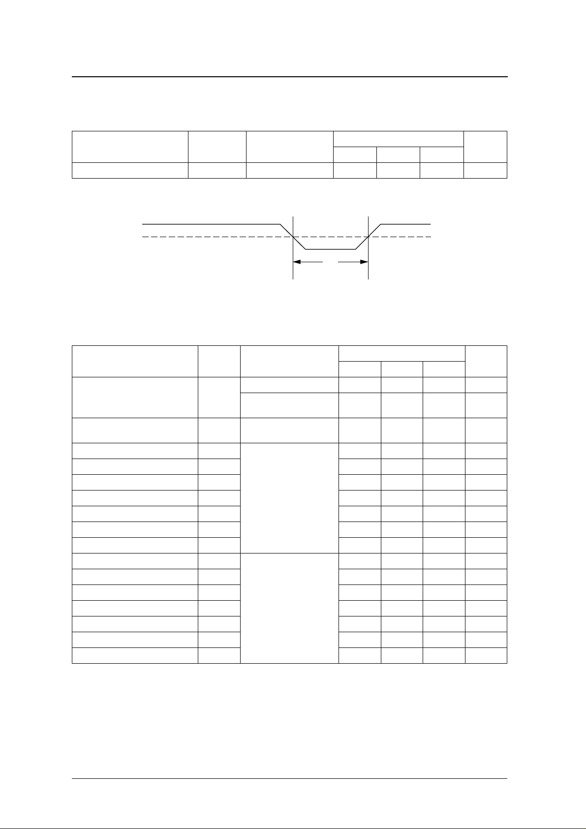
Reset timing (RSTN)
SM5847AF
VDD = V
= 3.00 to 5.25 V, VSS = V
DDAC
= 0 V, Ta = −40 to 85 °C
SSAC
Parameter Symbol Condition
RSTN LOW-level reset pulsewidth t
1. t
is equal to 1/f
MCK
XTI
or 1/f
. For example, t
OSC
RST
= 54 ns when f
RST
= 37 MHz.
XTI
RSTN
Output timing (CKO, BCKO, WCKO, DOL, DOR, DG)
VDD = V
XTI falling edge to CKO falling edge delay t
BCKO falling edge to WCKO, DOL, DOR,
DG delay
B C K O r ising edge to W CK O falling edge t
W CK O falling edge to BCKO rising edge t
BC KO per iod t
BC KO HIGH-level pulsewidth t
B CK O L OW -level pulsewidth t
DOL, DOR setup time t
DOL, DOR hold time t
B C K O r ising edge to W CK O falling edge t
W CK O falling edge to BCKO rising edge t
BC KO per iod t
BC KO HIGH-level pulsewidth t
B CK O L OW -level pulsewidth t
DOL, DOR setup time t
DOL, DOR hold time t
= 4.75 to 5.25 V, VSS = V
DDAC
= 0 V, Ta = −40 to 70 °C, CL = 50 pF
SSAC
Parameter Symbol Condition
XTO
VDD = V
DDAC
Ta = −40 to 85 °C
t
BDO
WOH
Output mode: 8fs
WOS
OBCY
OBCH
OBCL
ODS
ODH
WOH
WOS
OBCY
OBCH
OBCL
ODS
ODH
OMD = HIGH (fs = 192 kHz)
External clock input:
XTI = 27 ns (37 MHz),
CKSLN = HIGH (192fs)
Divider ratio: 1
CK DV1 = CKDV2 = LOW
Output data length: 24 bits
OW1N = OW2N = LOW
Output mode: 4fs
OMD = LOW (fs = 192 kHz)
External clock input:
XTI = 27 ns (37 MHz),
CKSLN = HIGH (192fs)
Divider ratio: 1
CK DV1 = CKDV2 = LOW
Output data length: 24 bits
OW1N = OW2N = LOW
= 3.00 to 5.25 V,
1
min
2t
MCK
tRST
min typ max
4–9ns
4–11ns
−
4– 2ns
8––ns
8––ns
27 – – ns
7––ns
7––ns
7––ns
7––ns
17 – – ns
17 – – ns
54 – – ns
18 – – ns
18 – – ns
18 – – ns
18 – – ns
Rating
typ ma x
Unit
––ns
1.5V
Rating
Unit
NIPPON PRECISION CIRCUITS—9
 Loading...