

NPC SM5844AF Datasheet
SM5844AF
NIPPON PRECISION CIRCUITS LTD.
Asynchronous Sample Rate Converter
OVERVIEW
The SM5844AF is a digital audio signal,
asynchronous sample rate converter LSI. It reads 16
or 20-bit word length input data, and writes 16, 18,
or 20-bit word length output data. It also features a
built-in digital deemphasis filter and digital
attenuator.
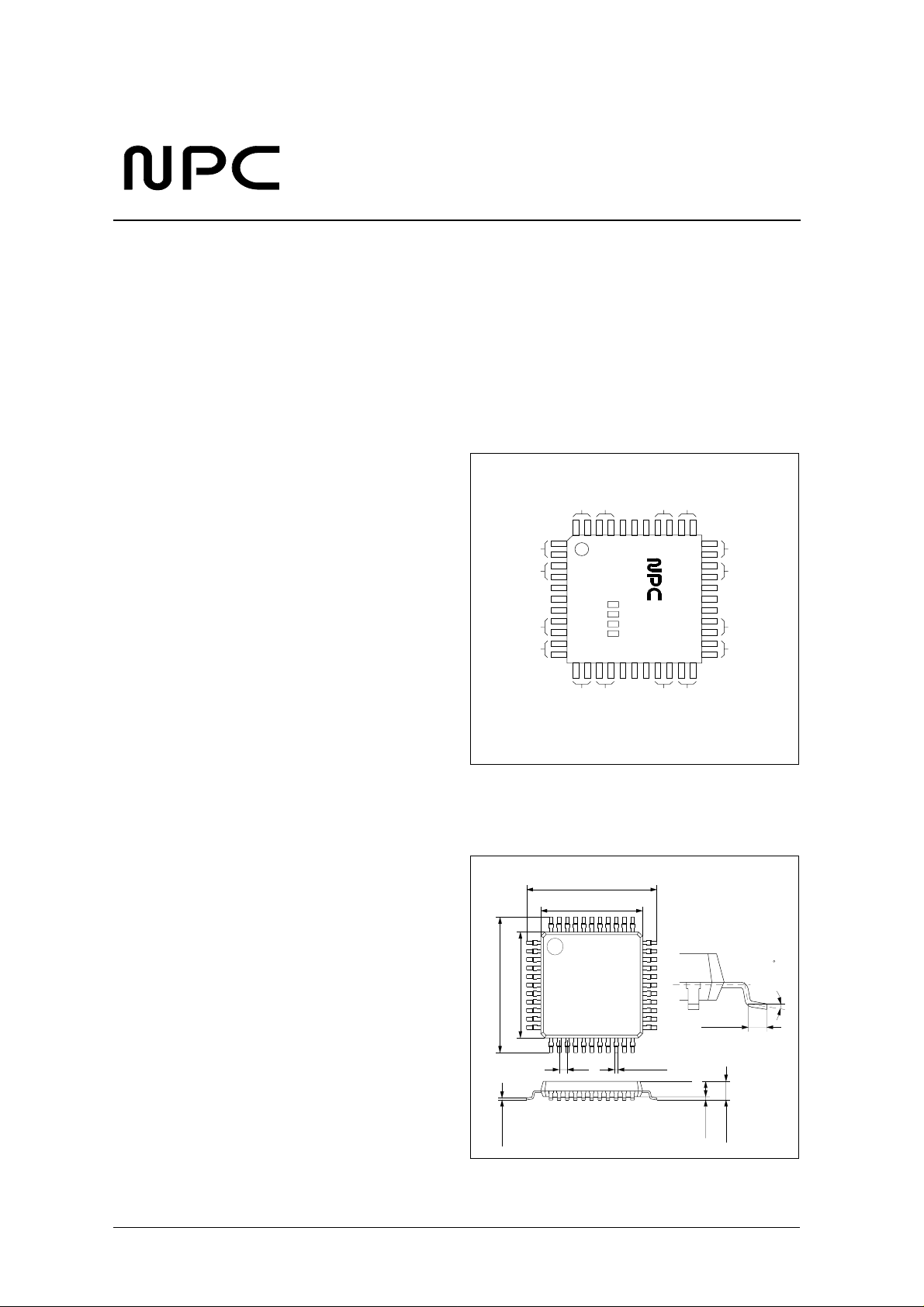
The SM5844AF operates from a 5 V supply, and is
available in 44-pin QFPs.
FEATURES
Functions
■
Left/right-channel processing (stereo)
Input sample rate (fsi) ranges
■
• 24 to 48 kHz (256fsi mode)
• 27 to 55 kHz (384fsi mode)
Output sample rate (fso) range
■
• 20 to 100 kHz
Sample rate conversion ratio (fso/fsi)
■
• 0.5 to 2.0 times
Asynchronous input and output timing (clock
■
inputs)
System clock inputs (input and output clocks
■
independent)
• 256fsi or 384fsi input system clock
• 256fso or 384fso output system clock
Deemphasis filter
■
• IIR-type filter
• 44.1, 48 or 32 kHz
Digital attenuator
■
• 11-bit data for 1025 levels
• Smooth, incremental attenuation change
• +12 dB gain shift function
Direct mute function
■
Through mode operation
■
• Input to output direct
Output data clocks (LRCO, BCKO)
■
• External input (slave mode)
• Output system clock generated internally
(master mode)
CMOS-level input/outputs
■
5 V (standard) single supply
■
44-pin QFP
■
Molybdenum-gate CMOS process
■
APPLICATIONS
■
Digital audio equipment, sample rate conversion
(audiovisual amplifiers, CD-R, DAT, MD and 8
mm VTRs)
■
Commercial recording/editing equipment, sample
rate conversion
■
Input data jitter elimination
PINOUT
THRUN
OCKSL
MDT/FSI2
MLEN/DEEM
SLAVE
OW18N
VSS
RSTN
TST2N
TST1N
STATE
IISN
OW20N
BCKI
ICKSL
IFM1
IFM2
DI
LRCI
ICLK
DOUT
VDD
BCKO
DMUTE
OCLK
LRCO
SM5844AF
MCOM
MDT/FSI1
PACKAGE DIMENSIONS
Unit: mm
44-pin QFP
+
12.80 0.30
-
10.00
-
+
10.00
12.80 0.30
+
0.60 0.20
-
+
0.35 0.10
-
1.45
0 to 0.20
1.75MAX
+
0.80
-
0.17 0.05
0 to 10
NIPPON PRECISION CIRCUITS—1
SM5844AF
Filter Characteristics and Converter
Efficiency
20-bit internal data word length
■
Deemphasis filter characteristics (IIR filter)
■
• ±0.03 dB gain deviation from ideal filter
characteristics
Converter noise levels
■
• ≤ − 110 dB internally-generated noise
• − 98 dB (16-bit output), − 110 dB (18-bit output)
and − 122 dB (20-bit output) word rounding
noise
■
Anti-aliasing LPF characteristics (4 FIR filters)
with automatic output/input sample rate
conversion ratio selection
• Up converter LPF (1.0 to 2.0 times)
• Down converter LPF 1 (48.0 to 44.1 kHz or
0.92 times)
• Down converter LPF 2 (44.1 to 32.0 kHz or
0.73 times)
• Down converter LPF 3 (48.0 to 32.0 kHz or
0.67 times)
■
Output S/N ratio (theoretical values)
Output signal word
length
16 bits 94.8 dB 97 dB
18 bits 97.5 dB 106 dB
20 bits 97.7 dB 109 dB
16-bit input word
length
S/N ratio
20-bit input word
length
Interfaces
■
Input data format
• 2s-complement, L/R alternating, serial
• Normal format (non IIS)
Mode Word length
1 16 bits
20 bits3 Front
4 Rear LSB first
■
Output data format
Front/rear
packing
Rear
• 2s-complement, MSB first, L/R alternating,
serial
• Continuous bit clock
Mode Word length IIS selection
1 16 bits
Nor mal (non
3 20 bits
4 20 bits
5 16 bits
7 20 bits
IIS)
IIS6 18 bits
Data
sequence
MSB first2
Front/rear
packing
Rear2 18 bits
Front
NIPPON PRECISION CIRCUITS—2
BLOCK DIAGRAM
SM5844AF
IFM1 IFM2 BCKI DI
MCOM
MDT/FSI1
MCK/FSI2
MLEN/DEEM
ICLK
ICKSL
LRCI
RSTN
TST1N
TST2N
Deemphasis and
attenuator setup
Input-stage
divider
Input timing
controller
Filter characteristic
select
Output operation
timing controller
Input data
interface
Arithmetic
operations
Deemphasis
operation
Attenuator
Interpolation
filter operation
Output
operation
OW18N
OW20N
IISN
SLAVE
OCLK
OCKSL
THRUN
DMUTE
Output format
controller
Output-stage
clock select
Output-stage
divider
Mute
generator
Dither
LRCO BCKO DOUT
Output data
interface
LRCI BCKI DI
Through mode
switching
Direct mute
STATE
NIPPON PRECISION CIRCUITS—3
PIN DESCRIPTION
SM5844AF
1
Number
1, 2 DI Ip Data input
3, 4 BCKI Ip Input bit clock
5 LRCI
6 ICLK I Input system clock input
7 ICKSL Ip Input system clock (ICLK) select. 384fsi when HIGH, and 256fsi when LOW .
8, 9 IFM1 Ip
10, 11 IFM2 Ip
12, 13 V DD – 5 V supply pin
14, 15 DMUTE Ip Direct mute pin
16 MCOM Ip
17 MDT/FSI1 Ip
18 MCK/FSI2 Ip
Name I/O
3
2
Ip Input word clock (fsi)
Input format select
IFM1 IFM2 W ord length Data sequence Data position
L O W L O W 16 bits
LOW HIGH
HIGH HIGH LSB first Rear packed
Interface switch control pin. M D T, MCK and MLEN control when HIGH. FSI1, FSI2 and DEEM
control when LOW.
When MCOM is HIGH: Microcontroller interface
data input (MDT)
When MCOM is HIGH: Microcontroller interface
bit clock (MCK)
Description
MSB first
20 bitsHIGH LOW Front packed
When MCOM is LOW: Deemphasis frequency
set pins
FSI1 FSI2 fsi
LOW HIGH 48.0 kHz
×
HIGH HIGH 32.0 kHz
Rear packed
LO W 44.1 kHz
19, 20 MLEN/DEEM Ip
21, 22 OW18N Ip
23, 24 OW20N Ip
25, 26 IISN Ip IIS output mode select. Normal mode when HIGH, and IIS mode when LOW .
27 S TAT E O Internal operation status output (for operation check)
28 TST1N Ip Output dither control. Dither ON when LOW, and OFF when HIGH.
29 TST2N Ip Test pin. Test mode when LOW. Normal operating mode when HIGH.
When MCOM is HIGH: Microcontroller data word latch clock (MLEN)
When MCOM is LOW: Deemphasis ON/OFF control (DEEM)
Output format select
When IISN = HIGH (normal mode)
OW20N OW18N Word length Data position
LOW LOW
20 bits
LOW HIGH
HIGH HIGH 16 bits
When IISN = LOW (IIS mode)
OW20N OW18N Word length Data position
LOW LOW
20 bits
LOW HIGH
HIGH LOW 18 bits
HIGH HIGH 16 bits
Front packed
Rear packedHIGH LOW 18 bits
IIS mode
Front packed
NIPPON PRECISION CIRCUITS—4
+
−
−
−
°
°
−
°
SM5844AF
Number
1
Name I/O
2
Description
30, 31 RSTN Ip Reset pin
32, 33 VS S – 0 V ground pin
34, 35 SL AV E Ip
BC KO and LRCO mode set. Outputs (master mode) when LOW, and inputs (slave mode) when
HIGH.
36, 37 T H RUN Ip DOUT through mode set. Normal mode when HIGH, and through mode when LOW.
38 OCKSL Ip Output system clock (OCLK) select. 384fso when HIGH, and 256fso when LOW .
39 OCLK I Output system clock input
40 LRCO
3
I/O Output word clock input/output (fso). Input/output mode set by the level on SLAV E.
41, 42 B C K O I/O Output bit clock input/output. Input/output mode set by the level o n S LAVE .
43, 44 DOUT O Data output
1. Pins which have the same name are connected internally. Accordingly, circuit connections can be made to either pin or to both pins.
2. I = input, Ip = Input with pull-up resistor (HIGH-level pins can be left open), O = output, I/O = input/output
3. fsi is the input word clock (LRCI) frequency, and fso is the output word clock (LRCO) frequency.
SPECIFICATIONS
Absolute Maximum Ratings
V
= 0 V
SS
Parameter Symbol Rating Unit
Supply voltage range V
Input voltage range V
Storage temperature range T
Po w er dissipation P
Soldering temperature T
Soldering time t
DD
IN
stg
D
sld
sld
0.3 to 7.0 V
0.3 to V
0.3 V
DD
40 to 125
550 m W
255
10 s
C
C
Recommended Operating Conditions
V
= 0 V
SS
Parameter Symbol Rating Unit
Supply voltage range V
Operating temperature range T
DD
opr
4.75 to 5.5 V
20 to 70
C
NIPPON PRECISION CIRCUITS—5
DC Electrical Characteristics
−
V
= 4.75 to 5.5 V, V
DD
= 0 V, T
SS
= − 20 to 70 ° C
a
SM5844AF
−
Ω
Parameter Symbol Condition
Current consumption I
HIGH-level input voltage
L O W -level input voltage
AC-coupled input voltage
HIGH-level output voltage
L O W-level output voltage
HIGH-level input current
L O W -level input current
Input leakage current
Pull-up resistance
1. ICKSL = LOW, OCKSL = LOW, f
2. Pins ICLK and OCLK.
2,3
2,3
2
4
4
2
2,3
3
3
= 13.0 MHz, f
ICLK
min typ max
DD
V
IH
V
IL
V
ACI
V
OH
V
OL
I
IH
I
IL
I
LH
R
IH
V
DD
I
OH
I
OL
V
IN
V
IN
V
IN
= 13.0 MHz, no output load
OCLK
1
= 5.0 V
––80mA
0.7V
DD
– – 0.3V
0.3V
DD
=
1.0 mA V
DD
= 1.0 mA – – 0.4 V
= V
DD
–1020µA
= 0 V – 1 0 2 0 µA
= V
DD
– – 1.0 µ A
250 500 1000 k
Rating
Unit
––V
DD
––V
0.5 – – V
V
p-p
3. Pins DI, BCKI, LRCI, ICKSL, IFM1, IFM2, DMUTE, MCOM, MDT/FSI1, MCK/FSI2, MLEN/DEEM, OW18N, OW20N, IISN, TST1N, TST2N, RSTN,
TH RUN, OCKSL and SLAVE.
4. Pins DOUT, BCKO, LRCO and STATE.
AC Electrical Characteristics
V
= 4.75 to 5.5 V, V
DD
ICLK input
= 0 V, T
SS
= − 20 to 70 ° C
a
Parameter Symbol
L O W -level clock
pulsewidth
HIGH-level clock
pulsewidth
Clock pulse cycle t
OCLK input
Parameter Symbol
L O W -level clock
pulsewidth
HIGH-level clock
pulsewidth
Clock pulse cycle t
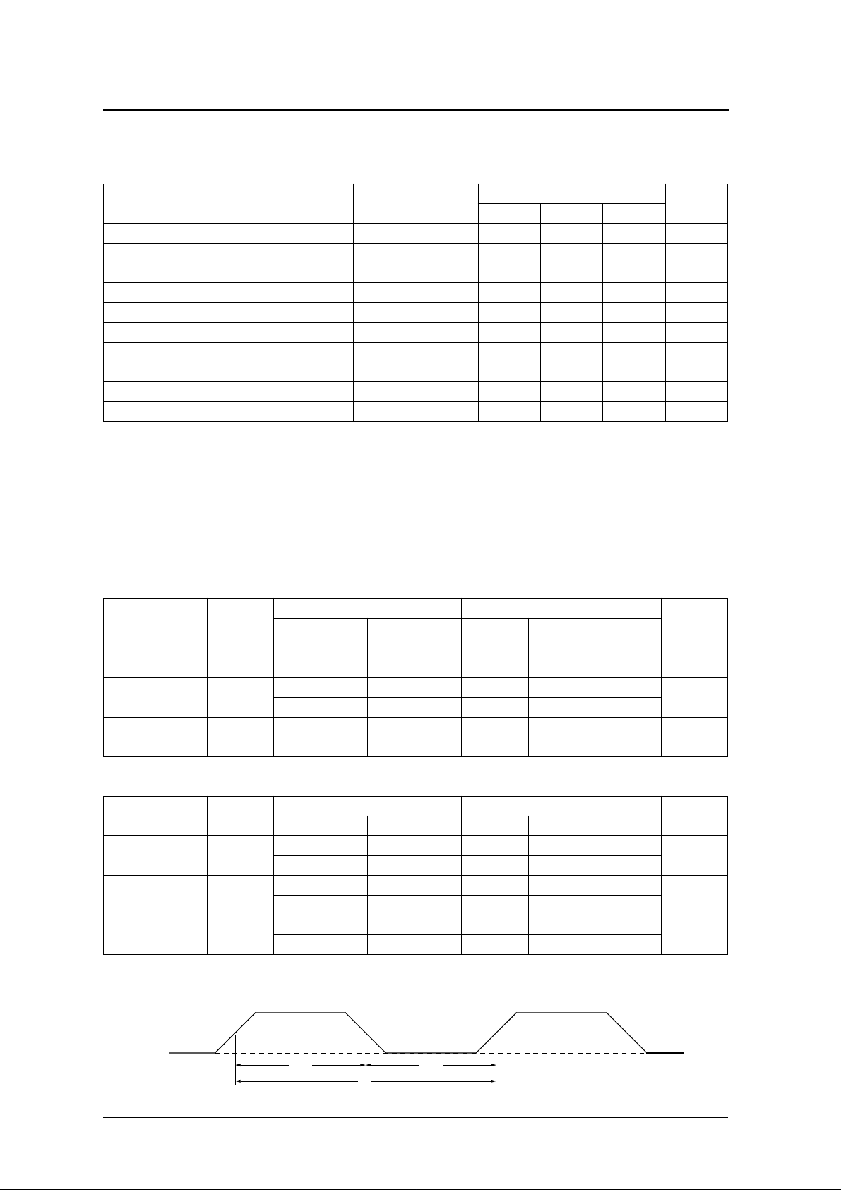
ICLK and OCLK timing
ICLK
OCLK
t
CWL
t
CWH
CY
t
CWL
t
CWH
CY
Condition Rating
ICKSL System clock min typ m ax
L OW 256fsi 30 – –
HIGH 384fsi 10 – –
L OW 256fsi 30 – –
HIGH 384fsi 10 – –
L OW 256fsi 80 – 162
HIGH 384fsi 47 – 106
Condition Rating
OCKSL System clock min typ m ax
LO W 256fso 15 – –
HIGH 384fso 10 – –
LO W 256fso 15 – –
HIGH 384fso 10 – –
LO W 256fso 39 – 200
HIGH 384fso 26 – 130
t
CWH
t
CY
t
CWL
Unit
ns
ns
ns
Unit
ns
ns
ns
>0.7V
0.5V
<0.3V
DD
DD
DD
NIPPON PRECISION CIRCUITS—6
BCKI, DI, LRCI inputs
SM5844AF
Parameter Symbol
BCKI LOW-level pulsewidth t
BCKI HIGH-level pulsewidth t
BCKI pulse cycle t
DI setup time t
DI hold time t
Last BCKI rising edge to LRCI edge t
LRCI edge to first BCKI rising edge t
BCKI, DI, LRCI timing
BCKI
t
DS
DI
BCWL1
BCWH1
BCY1
DS
DH
BL1
LB1
Rating
min typ max
50 – – ns
50 – – ns
100 – – ns
50 – – ns
50 – – ns
50 – – ns
50 – – ns
t
BCY1
t
BCWH1
t
DH
t
BCWL1
Unit
0.5V
0.5V
DD
DD
t
BL1
LRCI
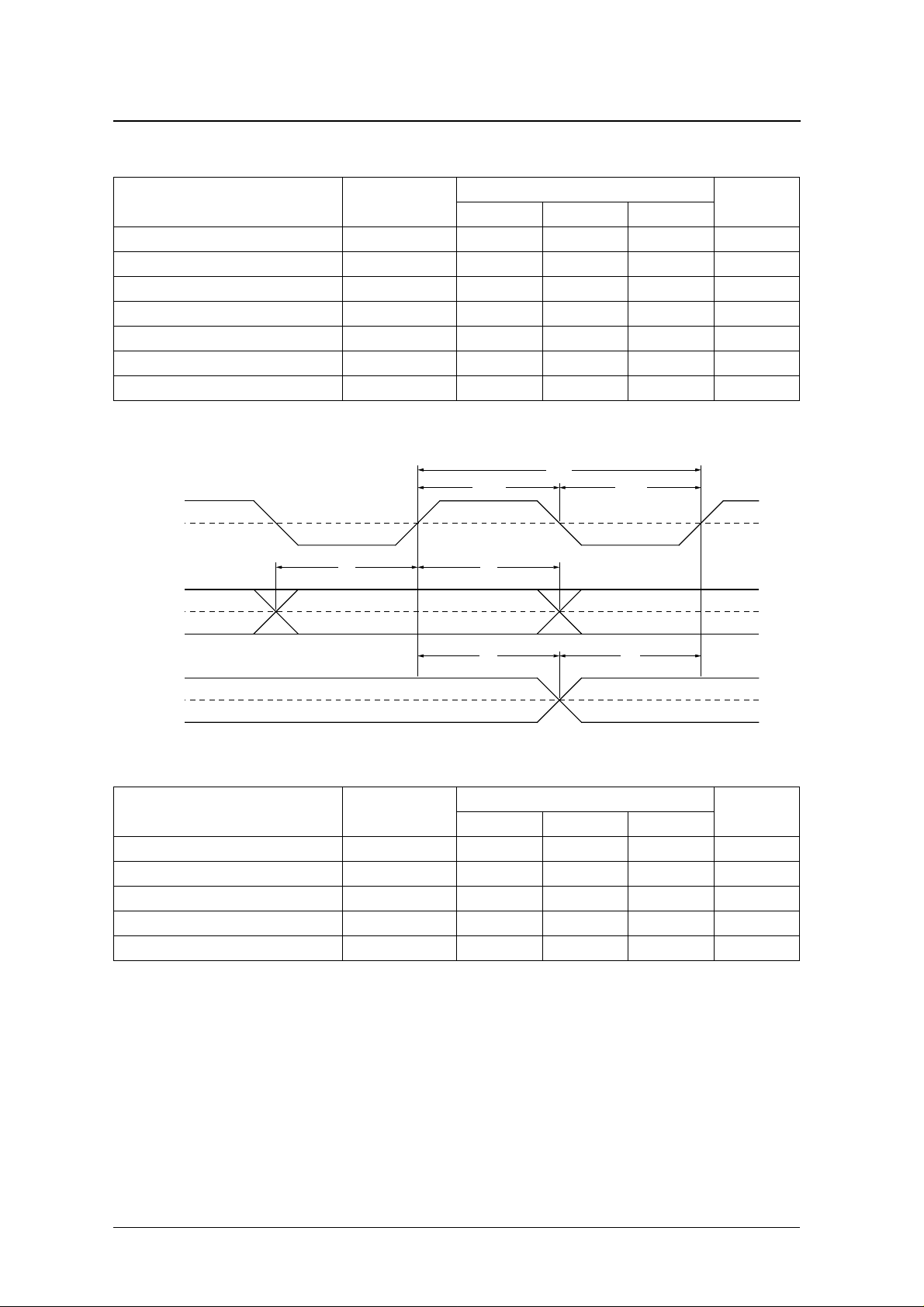
BCKO, LRCO (Inputs when SLAVE = HIGH)
Parameter Symbol
B CK O L OW -level pulsewidth t
BC KO HIGH-level pulsewidth t
B C KO pulse cycle
1
Last BCKO rising edge to LRCO edge t
LRCO edge to first BCKO rising edge t
BCWL2
BCWH2
t
BCY2
BL2
LB2
1. BCK O clock inputs exceeding 64fso cannot be detected, and will cause incorrect operation.
min typ max
78 – – ns
78 – – ns
156 – – ns
78 – – ns
78 – – ns
Rating
t
LB1
0.5V
DD
Unit
NIPPON PRECISION CIRCUITS—7
BCKO, LRCO timing
SM5844AF
t
BCWH2
t
BCY2
t
BCWL2
BCKO
t
BL2
LRCO
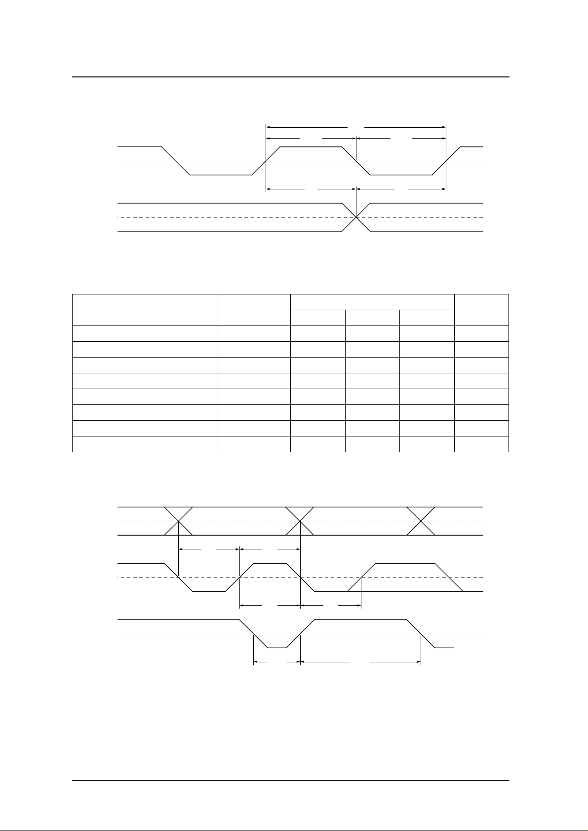
MDT, MCK, MLEN inputs
Parameter Symbol
MCK and MLEN rise time
MCK and MLEN fall time
MDT setup time t
MDT hold time t
MLEN setup time t
MLEN hold time t
MLEN LOW-level pulsewidth t
MLEN HIGH-level pulsewidth t
1
1
t
r
t
f
MDS
MDH
MCS
MCH
MEWL
MEWH
1. tr and tf are the input waveform transition times measured between 0.1VDD and 0.9VDD levels.
min typ max
– – 100 ns
– – 100 ns
50 – – ns
50 – – ns
50 – – ns
50 – – ns
50 – – ns
50 – – ns
Rating
0.5V
DD
t
LB2
0.5V
DD
Unit
MDT, MCK, MLEN timing
MDT
MCK
MLEN
t
MDS
t
MDH
t
MCS
t
MEWL
t
MCH
t
MEWH
0.5V
0.5V
0.5V
DD
DD
DD
NIPPON PRECISION CIRCUITS—8
 Loading...