NPC SM5842AP Datasheet

SM5842AP/APT
NIPPON PRECISION CIRCUITS INC.
High-Class Audio Multi-function Digital Filter
OVERVIEW
The SM5842AP/APT is a multi-function digital filter
IC, fabricated using NPC’s Molybdenum-gate
CMOS process, for digital audio reproduction equipment. It features 8-times oversampling (interpolation), independent left and right-channel digital
deemphasis, and soft muting functions. It accepts 16,
18, 20 or 24-bit input data, and outputs data in 18,
20, 22 or 24-bit format. It operates using either a
384fs or 256fs system clock at sampling frequencies
up to 48 kHz + 10% (384fs SM5842AP, 384/256fs
SM5842APT).
FEATURES
Functions
L/R 2-channel processing
■
8-times oversampling (interpolation)
■
• ≤ ±0.00002 dB passband ripple
• ≥ 117 dB stopband attenuation
Digital deemphasis
■
• 32/44.1/48 kHz sampling frequency (fs)
• 2-channel independent ON/OFF control
Soft muting
■
• 2-channel independent ON/OFF control
Input data format
■
• 2s complement, MSB first
- LR alternating, 16/18/20/24-bit serial, trailing data
- LR alternating, 24-bit serial, leading data
- LR simultaneous, 24-bit serial, leading data
Output data format
■
• 2s complement, MSB first, LR simultaneous
• 18/20/22/24-bit serial
• BCKO burst (NPC format)
Dither round-up processing
■
• ON (dither rounding)/OFF (normal rounding)
control
25-bit internal data length
■
Jitter-free function for correct operation in the
■
presence of jitter between the system clock and
LRCI clock
• ON (jitter-free mode)/OFF (sync mode) control
256fs/384fs system clock selectable
■
• 384fs
- 21.2 MHz maximum frequency (at maximum
fs = 55.2 kHz)
• 256fs
- 13 MHz maximum frequency (at maximum
fs = 50.7 kHz, SM5842AP)
- 14.2 MHz maximum frequency (at maximum
fs = 55.2 kHz, SM5842APT)
■
Crystal oscillator circuit built-in
■
TTL-compatible input/outputs
■
5.0 ± 0.25 V supply
■
Molybdenum-gate CMOS process
■
28-pin plastic DIP
Filter Configuration
■
Linear phase 3-stage FIR interpolation filter
• 169-tap 1st stage (fs to 2fs)
• 29-tap 2nd stage (2fs to 4fs)
• 17-tap 3rd stage (4fs to 8fs)
■
Deemphasis filter
- IIR filter configuration for accurate gain and
phase characteristics
■
26 × 24-bit parallel multiplier/32-bit accumulator
for high precision
■
Overflow limiter built-in
APPLICATIONS
■
CD players
■
DAT players
■
PCM systems
PINOUT
DI / INF2N
BCKI
CKSLN
INF1N
IW1N / DIL
XTI
XTO
VSS
CKO
IW2N / DIR
OW1N
OW2N
SYNCN
RSTN
1
SM5842AP/APT
14
LRCI
28
DG
BCKO
WCKO
DOL
DOR
VDD
DITHN
MUTEL
MUTER
FSEL2
FSEL1
DEMPL
DEMPR
15
NIPPON PRECISION CIRCUITS—1
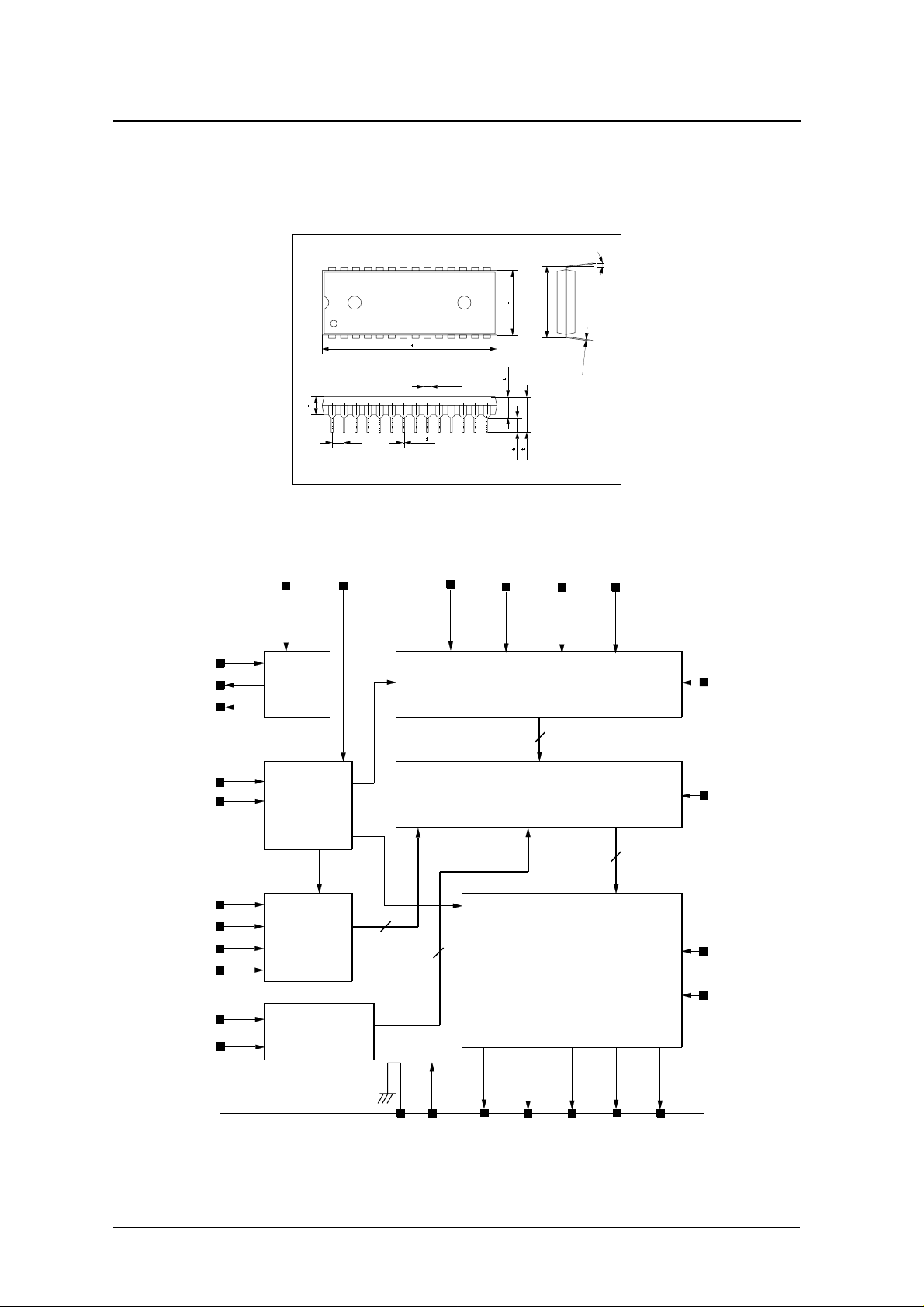
PACKAGE DIMENSIONS
Unit: mm
28-pin plastic DIP
SM5842AP/APT
13.8 0.2
0° to 15°
15.2
BLOCK DIAGRAM
XTI
XTO
CKO
RSTN
SYNCN
3.8 0.1
CKSLN LRCI
System
Clock
Timing
Controller
37.3 0.3
+
0.3
1.5
0.05
−
2.54
0.45 0.1
DI
/ INF2N
4.5 0.3
BCKI
3.2 0.2
3.2 0.2
7.7 0.5
Input Data Interface
Filter and Attenuation Arithmetic block
IW1N
/ DIL
0.10
0.05
+
−
0.25
IW2N
/ DIR
INF1N
DITHN
DEMPL
DEMPR
FSEL1
FSEL2
MUTEL
MUTER
Deemphasis
Control
Mute Control
BCKO WCKO DGDORDOL
V
DDVSS
OW1N
Output Data Interface
OW2N
NIPPON PRECISION CIRCUITS—2
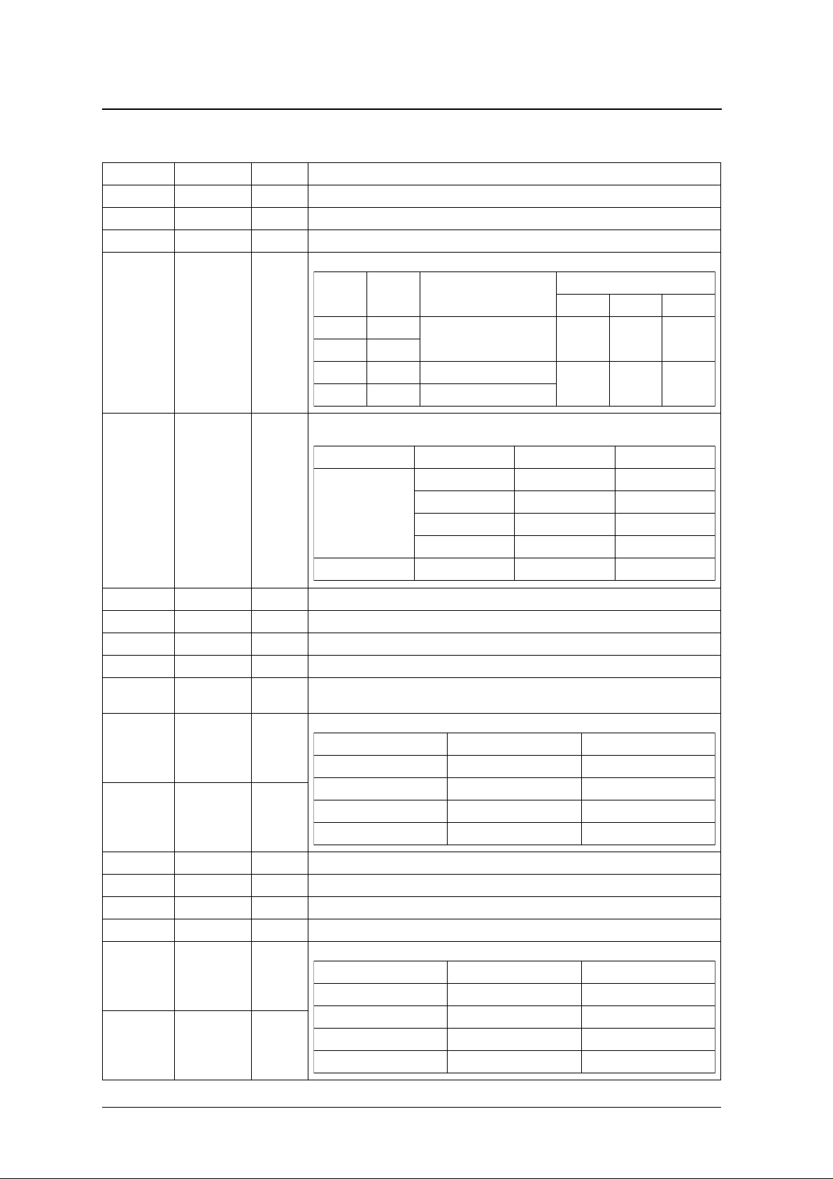
PIN DESCRIPTION
SM5842AP/APT
Number Name I/O
1 DI/INF2N Ip Data input when INF1N is LOW, and input format select pin 2 when INF1N is HIGH.
2 BCKI Ip Input bit clock
3 CKSLN Ip Oscillator and system clock select input. 384fs when HIGH, and 256fs when LOW.
4 INF1N Ip
5 IW1N/DIL Ip
1
Input format select pin 1. INF1N and INF2N select the pin functions below.
INF1N DI/INF2N Input format
LOW LOW
LR alternating, trailing data DI IW1N IW2N
LOW HIGH
HIGH LOW LR alternating, leading data
HIGH HIGH LR simultaneous, leading data
Input bit length select pin 1 when INF1N is LOW, and left-channel data input when INF1N is HIGH.
IW1N and IW2N select the input data length.
INF1N IW2N/DIL IW1N/DIR Input bit length
LOW
HIGH ××24 bits
Description
Pin function selection
DI/INF2N IW1N/DIL IW2N/DIR
INF2N DIL DIR
LOW LOW 24 bits
LOW HIGH 20 bits
HIGH LOW 18 bits
HIGH HIGH 16 bits
6 XTI I Oscillator input connection
7 XTO O Oscillator output connection
8 VSS – Ground
9 CKO O Oscillator output clock. Same frequency as XTI.
10 IW2N/DIR Ip
11 OW1N Ip
12 OW2N Ip
13 SYNCN Ip Sync mode select pin. Normal sync mode when LOW, and jitter-free mode when HIGH.
14 RSTN Ip System reset. Reset operation when LOW, and normal operation when HIGH.
15 DEMPR Ip Right-channel deemphasis control signal. OFF when LOW, and ON when HIGH.
16 DEMPR Ip Left-channel deemphasis control signal. OFF when LOW, and ON when HIGH.
17 FSEL1 Ip
18 FSEL2 Ip
Input bit length select pin 2 when INF2N is LOW , and right-channel data input when INF2N is HIGH.
IW1N and IW2N select the input data length as shown in the table for pin 5.
Output length select bits.
OW2N OW1N Output bit length
LOW LOW 24 bits
LOW HIGH 22 bits
HIGH LOW 20 bits
HIGH HIGH 18 bits
Deemphasis filter select inputs
FSEL1 FSEL2 Sampling frequency (fs)
LOW LOW 44.1 kHz
LOW HIGH 48 kHz
HIGH LOW Invalid setting
HIGH HIGH 32 kHz
NIPPON PRECISION CIRCUITS—3
SM5842AP/APT
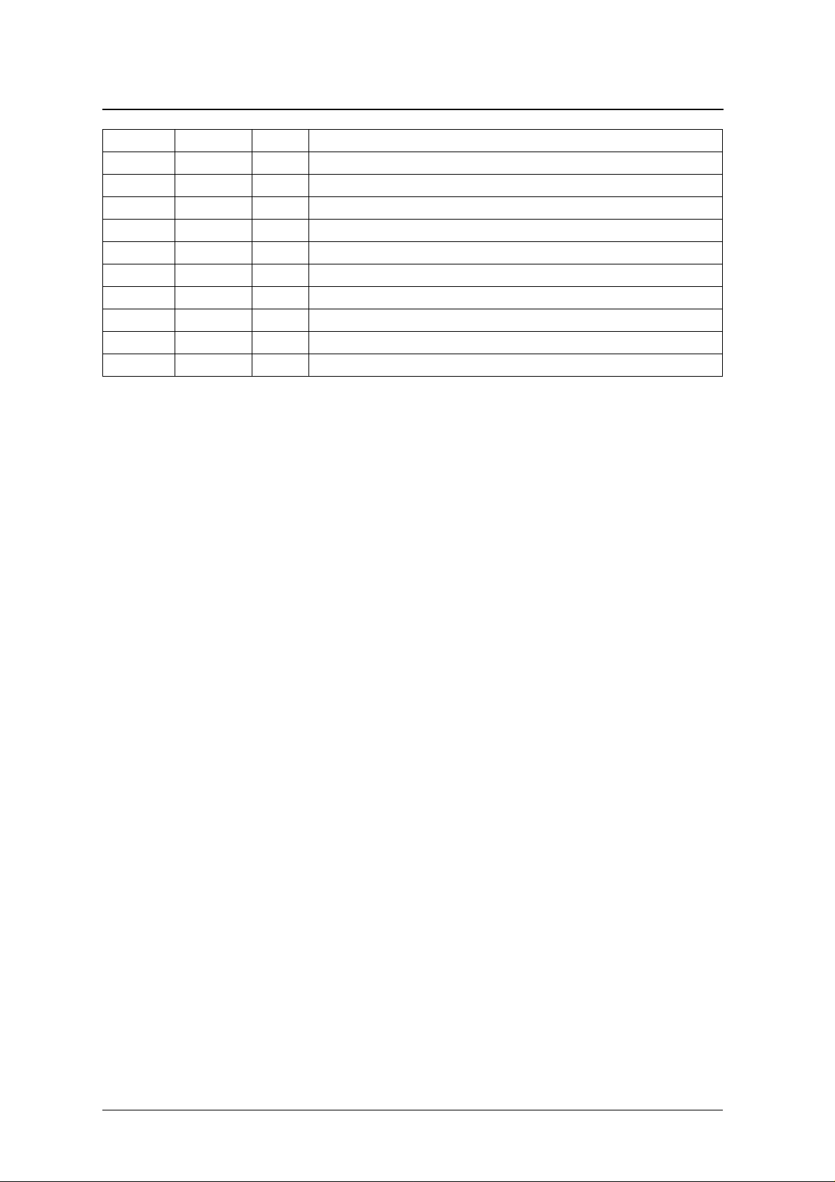
Number Name I/O
19 MUTER Ip Right-channel mute signal. Muting when HIGH, and normal output when LOW.
20 MUTEL Ip Left-channel mute signal. Muting when HIGH, and normal output when LOW.
21 DITHN Ip Dither processing control. ON when LOW, and OFF when HIGH.
22 VDD – 5 V supply
23 DOR O Right-channel data output
24 DOL O Left-channel data output
25 WCKO O Output word clock
26 BCKO O Output bit clock
27 DG O Deglitched output
28 LRCI Ip Input data sample rate (fs) clock
1. I = input, Ip = Input with pull-up resistor, O = output
1
Description
NIPPON PRECISION CIRCUITS—4
SM5842AP/APT
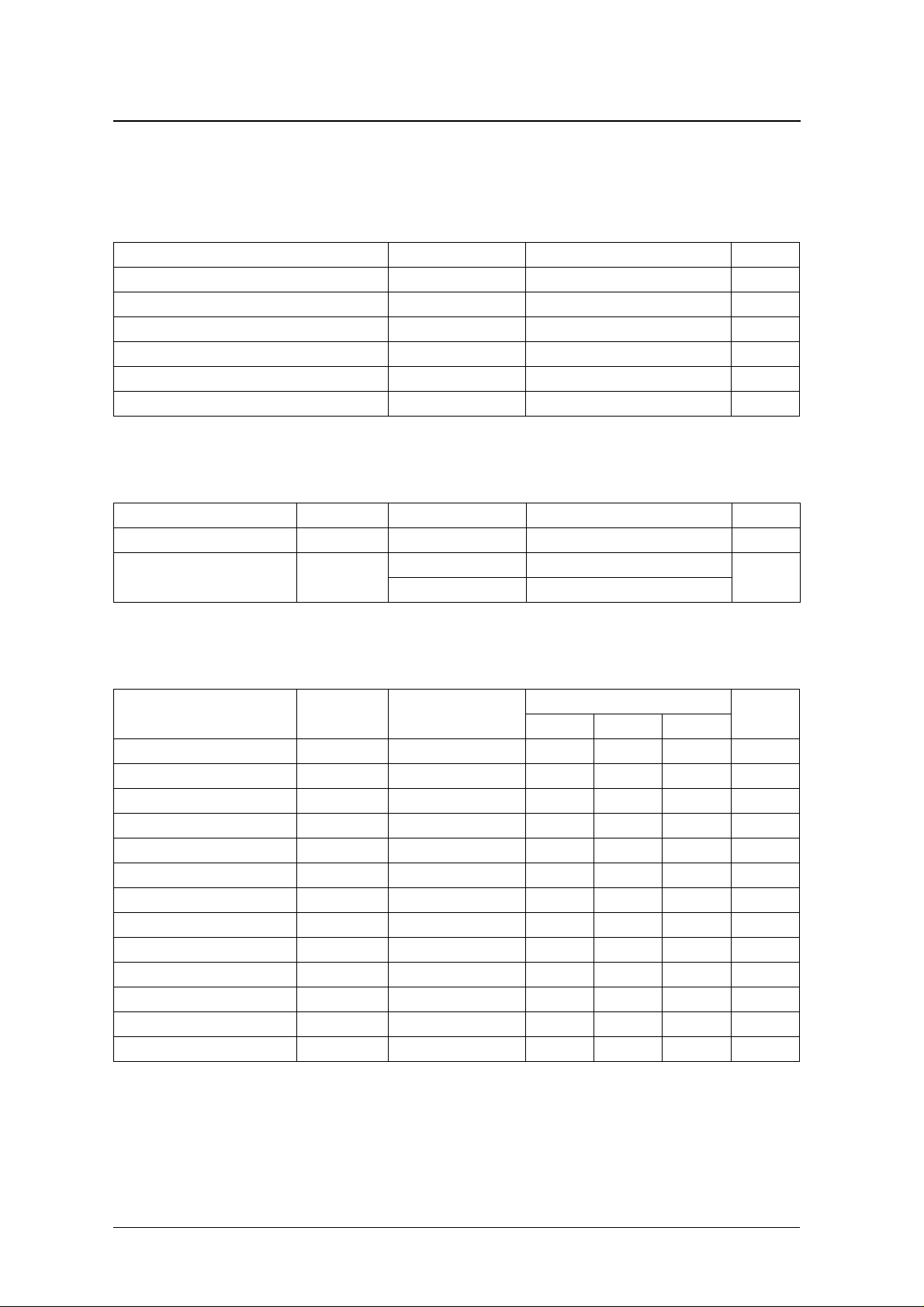
SPECIFICATIONS
Absolute Maximum Ratings
V
= 0 V
SS
Parameter Symbol Rating Unit
Supply voltage range V
Input voltage range V
Storage temperature range T
Power dissipation P
Soldering temperature T
Soldering time t
Recommended Operating Conditions
−
−
−
DD
IN
stg
D
sld
sld
0.3 to 7.0 V
0.3 to V
+ 0.3 V
DD
40 to 125
550 mW
255
10 s
° C
° C
V
= 0 V
SS
Parameter Symbol Condition Rating Unit
Supply voltage range V
Operating temperature range T
DD
SM5842AP
opr
SM5842APT
4.75 to 5.25 V
− 20 to 80
° C
− 20 to 70
DC Electrical Characteristics
V
= 4.75 to 5.25 V, V
DD
Parameter Symbol Condition
Current consumption I
XTI HIGH-level input voltage V
XTI LOW-level input voltage V
HIGH-level input voltage
LOW-level input voltage
2
2
HIGH-level output voltage
LOW-level output voltage
XTO HIGH-level output voltage V
XTO LOW-level output voltage V
XTI HIGH-level input current I
XTI LOW-level input current I
LOW-level input current
Input leakage current
1. f
= 256fs = 14.2 MHz (CKSLN = LOW), no output load
SYS
2. Pins DI/INF2N, BCKI, CKSLN, INF1N, IW1N/DIL, IW2N/DIR, OW1N, OW2N, SYNCN, RSTN, DEMPR, DEMPL, FSEL1, FSEL2, MUTER, MUTEL,
2
2
DITHN, LRCI
3. Pins CKO, DOL, DOR, BCKO, WCKO, DG
= 0 V, T
SS
= − 20 to 80 ° C
a
Rating
Unit
min typ max
DD
IH1
IL1
V
IH2
V
IL2
3
3
V
OH1
V
OL1
OH2
OL2
LH
LL1
I
LL2
I
IH
V
I
OH
I
OL
I
OH
I
OL
V
V
V
V
1
= 5.0 V
DD
= − 0.4 mA 2.5 – – V
= 1.6 mA – – 0.4 V
= − 1.0 mA V
= 1.0 mA – – 0.4 V
= V
IN
DD
= 0 V – 10 20 µA
IN
= 0 V – 10 20 µA
IN
= V
IN
DD
–6080mA
0.7V
DD
– – 0.3V
––V
DD
V
2.4 – – V
– – 0.5 V
− 0.5 – – V
DD
–1020µA
– – 1.0 µA
NIPPON PRECISION CIRCUITS—5
AC Electrical Characteristics
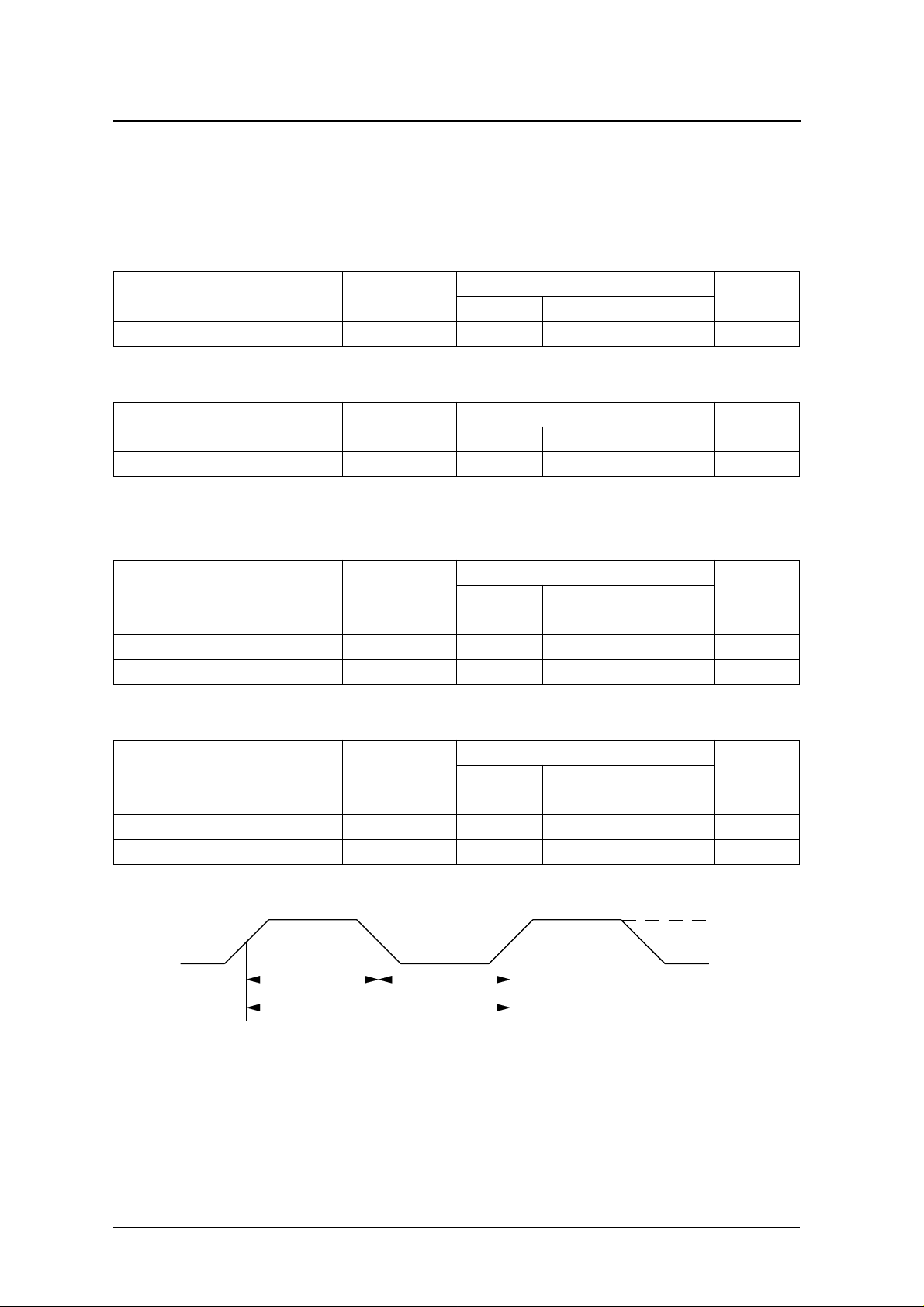
Input Clock (XTI: SM5842AP)
Crystal oscillator
SM5842AP/APT
fs = 384fs (CKSLN = HIGH): V
Parameter Symbol
Oscillator frequency f
fs = 256fs (CKSLN = LOW): V
Parameter Symbol
Oscillator frequency f
= 4.75 to 5.25 V, V
DD
= 4.75 to 5.25 V, V
DD
External clock input
fs = 384fs (CKSLN = HIGH): V
Parameter Symbol
Clock HIGH-level pulsewidth t
Clock LOW-level pulsewidth t
Clock pulse cycle time t
= 4.75 to 5.25 V, V
DD
OSC
OSC
CWH
CWL
XI
= 0 V, T
SS
= 0 V, T
SS
= 0 V, T
SS
= − 20 to 80 ° C
a
Rating
min typ max
2.0 – 21.2 MHz
= − 20 to 80 ° C
a
Rating
min typ max
1.0 – 13.0 MHz
= − 20 to 80 ° C
a
Rating
min typ max
20 – 250 ns
20 – 250 ns
47 – 500 ns
Unit
Unit
Unit
fs = 256fs (CKSLN = LOW): V
Parameter Symbol
Clock HIGH-level pulsewidth t
Clock LOW-level pulsewidth t
Clock pulse cycle time t
= 4.75 to 5.25 V, V
DD
XTI
tCWH tCWL
tXI
CWH
CWL
XI
= 0 V, T
SS
= − 20 to 80 ° C
a
Rating
min typ max
35 – 500 ns
35 – 500 ns
76 – 1000 ns
VIH1
0.5V
VIL1
Unit
DD
NIPPON PRECISION CIRCUITS—6
SM5842AP/APT
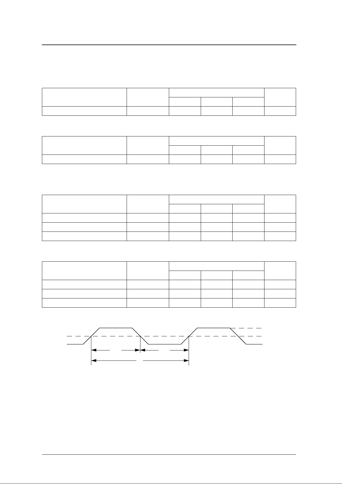
Input Clock (XTI: SM5842APT)
Crystal oscillator
fs = 384fs (CKSLN = HIGH): VDD = 4.75 to 5.25 V, VSS = 0 V, Ta = −20 to 70 °C
Parameter Symbol
Oscillator frequency f
OSC
min typ max
2.0 – 21.2 MHz
Rating
fs = 256fs (CKSLN = LOW): VDD = 4.75 to 5.25 V, VSS = 0 V, Ta = −20 to 70 °C
Parameter Symbol
Oscillator frequency f
External clock input
OSC
min typ max
1.0 – 14.2 MHz
Rating
fs = 384fs (CKSLN = HIGH): VDD = 4.75 to 5.25 V, VSS = 0 V, Ta = −20 to 70 °C
Parameter Symbol
Clock HIGH-level pulsewidth t
Clock LOW-level pulsewidth t
Clock pulse cycle time t
CWH
CWL
XI
min typ max
20 – 250 ns
20 – 250 ns
47 – 500 ns
Rating
fs = 256fs (CKSLN = LOW): VDD = 4.75 to 5.25 V, VSS = 0 V, Ta = −20 to 70 °C
Unit
Unit
Unit
Parameter Symbol
Clock HIGH-level pulsewidth t
Clock LOW-level pulsewidth t
Clock pulse cycle time t
XTI
tCWH tCWL
tXI
CWH
CWL
XI
Rating
min typ max
30 – 500 ns
30 – 500 ns
70 – 1000 ns
VIH1
0.5V
DD
VIL1
Unit
NIPPON PRECISION CIRCUITS—7
 Loading...