

SM5841H
NIPPON PRECISION CIRCUITS INC.
Audio Multi-function Digital Filter
OVERVIEW
The SM5841H is an 8-times oversampling (interpolation) digital filter for digital audio reproduction
equipment. It accepts 16 or 18-bit input data, and
outputs data in 16, 18 or 20-bit format, making a
wide range of interfaces possible. It also features
digital deemphasis for 3 sampling frequencies, a
noise shaper to reduce quantization noise, a DC offset output and other circuits.
FEATURES
Functions
■
2-channel processing
■
8-times (8fs) oversampling (interpolation)
■
Digital deemphasis (fs = 48/44.1/32 kHz)
■
Serial input data
2s complement, MSB first, 16/18-bit
■
Serial output data
2s complement, MSB first, 16/18/20-bit
■
1st-order noise shaper (for 16/18-bit output only)
■
256fs/384fs system clock selectable
■
Output data DC offset (approximately 0.8%)
ON/OFF control
■
TTL-compatible input/outputs
■
5 V (standard) supply
■
3.2 V operating voltage
■
Molybdenum-gate CMOS
ORDERING INFOMATION
Device Package
SM5841HP 18pin DIP
SM5841HS 22pin SOP
Filter Characteristics
■
3-stage DC FIR interpolation filter
1st stage (fs → 2fs), 69-tap
2nd stage (2fs → 4fs), 13-tap
3rd stage (4fs → 8fs), 9-tap
■
IIR deemphasis filter for gain and phase characteristics close to those of analog filters
■
Overflow limiter built-in
APPLICATIONS
■
Digital amplifiers
■
CD players
■
DAT players
■
DBS systems
■
PCM systems
NIPPON PRECISION CIRCUITS—1
SM5841H
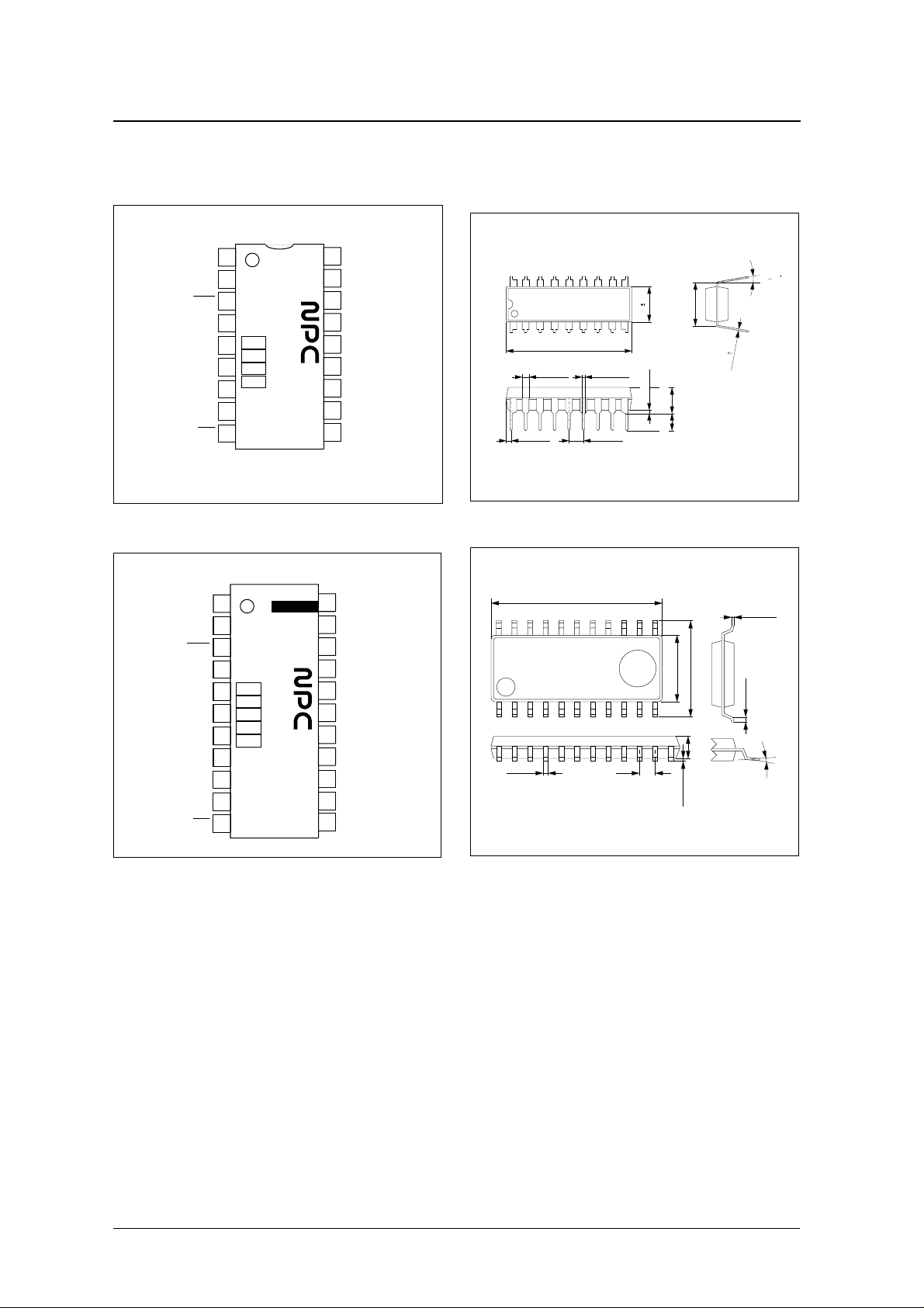
PINOUT
18-pin DIP
22-pin SOP
WSL1
CKSL
CKO
WSL2
DSF1
DSF2
WSL1
CKI
CKSL
CKO
VSS
(NC)
(NC)
WSL2
DSF1
DSF2
RST
CKI
VSS
RST
PACKAGE DIMENSIONS
18-pin DIP (Unit: mm)
DIN
1
2
3
SM5841HP
4
5
6
7
8
9
1
2
3
4
SM5841HS
5
6
7
8
9
10
11
18
17
BCKI
LRCI
16
OFST
15
14
VDD
WCKO
13
DOL
12
DOR
11
BCKO
10
1.27MAX 2.54TYP
1.20
22.05
+ 0.30
− 0
+ 0.20
− 0.30
0.45
+ 0.14
− 0.05
6.20 0.25
0.51MIN
7.62TYP
5.00MAX
3.00MIN
015
0.25 0.05
22-pin SOP (Unit: mm)
DIN
22
BCKI
21
LRCI
20
OFST
19
(NC)
18
(NC)
17
VDD
16
WCKO
15
DOL
14
DOR
13
BCKO
12
0.4 ± 0.1
13.9 ± 0.3
1.27
5.4 ± 0.2
7.8 ± 0.3
0.05 ± 0.05
1.8 ± 0.1
+ 0.1
0.15 − 0.05
0.5 ± 0.2
0 to 10˚
NIPPON PRECISION CIRCUITS—2
BLOCK DIAGRAM
SM5841H
LRCI BCKIDIN
CKSL
CKI
CKO
RST
DSF1
DSF2
WSL1
WSL2
PIN DESCRIPTION
SOP DIP Name I/O
1 1 WSL1 Ip
8 6 WSL2 Ip
System
Clock
Timing
Controller
Deemphasis
Controler
Input/output
word length
selector
VSS
1
Input/output data select pins
WSL1 WSL2 Noise shaper Input bit length Output bit length
HIGH HIGH Off 18 bits 20 bits
HIGH LOW On 18 bits 18 bits
LOW HIGH On 16 bits 18 bits
LOW LOW On 16 bits 16 bits
VDD
Input data Interface
Filter and Attenuation
Airthmetic block
Interface
Output date
Description
OFST
WCKO
DOL
DOR
BCKO
2 2 CKI Ip System clock input
3 3 CKSL
4 4 CKO O System clock output. The CKI is first buffered before output on CKO.
5 5 VSS – Ground
6 – NC – No connection
7 – NC – No connection
9 7 DSF1 Ip
10 8 DSF2 Ip
11 9 RST
12 10 BCKO O Output bit clock
Ip System clock select input. 384fs when HIGH, and 256fs when LOW.
Deemphasis select inputs
DSF1 DSF2 Deemphasis Sampling frequency
LOW LOW On 44.1 kHz
LOW HIGH On 48.0 kHz
HIGH LOW Off –
HIGH HIGH On 32.0 kHz
Ip System reset. Reset and initialization when RST is LOW.
NIPPON PRECISION CIRCUITS—3
−
−
+
−
°
°
−
° C
SM5841H
SOP DIP Name I/O
13 11 DOR O Right-channel 8fs data output
14 12 DOL O Left-channel 8fs data output
15 13 WCKO O Output word clock
16 14 VDD – 5 V supply
17 – NC – No connection
18 – NC – No connection
19 15 OFST Ip Output data DC offset select input. Summing ON when HIGH, and OFF when LOW.
20 16 LRCI Ip Input data sample rate (fs) clock
21 17 BCKI Ip Input bit clock
22 18 DIN Ip Input data
1. Ip = Input with pull-up resistor
1
Description
SPECIFICATIONS
Absolute Maximum Ratings
V
= 0 V
SS
Parameter Symbol Rating Unit
Supply voltage range V
Input voltage range V
Storage temperature range T
Power dissipation P
Soldering temperature T
Soldering time t
DD
IN
stg
D
sld
sld
0.3 to 7.0 V
0.3 to V
0.3 V
DD
40 to 125
250 mW
255
10 s
C
C
Recommended Operating Conditions
V
= 0 V
SS
Parameter Symbol Rating Unit
Supply voltage range V
Operating temperature range T
DD
opr
3.2 to 5.5 V
20 to 80
NIPPON PRECISION CIRCUITS—4
DC Electrical Characteristics
SM5841H
Standard voltage: V
= 4.5 to 5.5 V, V
DD
= 0 V, T
SS
Parameter Symbol Condition
Current consumption I
HIGH-level input voltage
LOW-level input voltage
2
2
CKI AC-coupled input voltage V
HIGH-level input voltage
LOW-level input voltage
HIGH-level output voltage
LOW-level output voltage
3
3
4
4
CKI HIGH-level input current I
CKI LOW-level input current I
LOW-level input current
Input leakage current
Input leakage current
1. f
= 384fs = 20 MHz, no output load
SYS
2. Pins CKSL
3
2, 3
2
, OFST
V
V
INAC
V
V
V
V
I
I
DD
IH1
IL1
IL2
LH
I
IH1
IL1
IH2
IL2
OH
OL
LL
3. Pins LRCI, DIN, BCKI, DSF1, DSF2, WSL1, WSL2, RST
4. Pins CKO, DOL, DOR, BCKO, WCKO
= − 20 to 80 ° C
a
Rating
min typ max
= 5.0 V
1
––40mA
0.7V
DD
– – 0.3V
DD
––V
DD
––V
V
DD
Sine wave input 0.3V
2.4 – – V
– – 0.5 V
I
= − 0.4 mA 2.5 – – V
OH
I
= 1.6 mA – – 0.4 V
OL
V
= V
IN
DD
V
= 0 V – 10 20 µA
IN
V
= 0 V – 10 20 µA
IN
V
= V
IN
DD
V
= 0 V – – 1.0 µA
IN
–1020µA
– – 1.0 µA
Unit
V
p-p
Low voltage: V
= 3.2 to 4.5 V, V
DD
= 0 V, T
SS
Parameter Symbol Condition
Current consumption I
HIGH-level input voltage
LOW-level input voltage
2
2
CKI AC-coupled input voltage V
HIGH-level input voltage
LOW-level input voltage
HIGH-level output voltage
LOW-level output voltage
3
3
4
4
CKI HIGH-level input current I
CKI LOW-level input current I
LOW-level input current
Input leakage current
Input leakage current
1. f
= 384fs = 18.5 MHz, no output load
SYS
2. Pins CKSL, OFST
3
2, 3
2
V
V
INAC
V
V
V
V
I
I
DD
IH1
IL1
IL2
LH
I
IH1
IL1
IH2
IL2
OH
OL
LL
3. Pins LRCI, DIN, BCKI, DSF1, DSF2, WSL1, WSL2, RST
4. Pins CKO, DOL, DOR, BCKO, WCKO
= − 20 to 80 ° C
a
Rating
min typ max
= 3.4 V
1
––20mA
0.7V
DD
– – 0.3V
DD
––V
DD
––V
V
DD
Sine wave input 0.3V
2.4 – – V
– – 0.5 V
I
= − 0.2 mA 2.5 – – V
OH
I
= 0.8 mA – – 0.4 V
OL
V
= V
IN
DD
V
= 0 V – – 12 µA
IN
V
= 0 V – – 12 µA
IN
V
= V
IN
DD
V
= 0 V – – 1.0 µA
IN
––12µA
– – 1.0 µA
Unit
V
p-p
NIPPON PRECISION CIRCUITS—5
AC Electrical Characteristics
Clock (CKI)
Standard voltage: V
Parameter Symbol
HIGH-level clock pulsewidth t
LOW-level clock pulsewidth t
Clock pulse cycle t
= 4.5 to 5.5 V, V
DD
CWH
CWL
CI
SM5841H
= 0 V, T
SS
CKSL
HIGH 384fs 23 – 250
LOW 256fs 35 – 500
HIGH 384fs 23 – 250
LOW 256fs 35 – 500
HIGH 384fs 50 – 500
LOW 256fs 76 – 1000
= −20 to 80 °C
a
Condition Rating
System
clock
min typ max
Unit
ns
ns
ns
Low voltage: VDD = 3.2 to 4.5 V, VSS = 0 V, Ta = −20 to 80 °C
Condition Rating
Parameter Symbol
HIGH-level clock pulsewidth t
LOW-level clock pulsewidth t
Clock pulse cycle t
CWH
CWL
CI
CKSL
HIGH 384fs 25 – 250
LOW 256fs 50 – 500
HIGH 384fs 25 – 250
LOW 256fs 50 – 500
HIGH 384fs 54 – 500
LOW 256fs 108 – 1000
System
clock
CKI
tCWH
tCWL
tCI
min typ max
over
DD
0.7×V
0.5×V
DD
under
0.3×V
DD
Unit
ns
ns
ns
NIPPON PRECISION CIRCUITS—6

Serial input timing (BCKI, DI, LRCI)
VDD = 3.2 to 5.5 V, VSS = 0 V, Ta = −20 to 80 °C
SM5841H
Parameter Symbol
BCKI HIGH-level pulsewidth t
BCKI LOW-level pulse width t
BCKI pulse cycle t
DIN setup time t
DIN hold time t
Last BCKI rising edge to LRCI edge t
LRCI edge to first BCKI rising edge t
BCKI
DIN
BCWH
BCWL
BCY
DS
DH
BL
LB
tDS
Rating
min typ max
50 – – ns
50 – – ns
100 – – ns
50 – – ns
50 – – ns
50 – – ns
50 – – ns
Unit
tBCY
tBCWH
tBCWL
1.5V
tDH
1.5V
LRCI
Reset timing (RST)
VDD = 3.2 to 5.5 V, VSS = 0 V, Ta = −20 to 80 °C
Parameter Symbol Condition
LOW-level reset pulse width t
RST
RST
At power-ON 1 – – µs
At all other times 50 – – ns
Control inputs (DSF1, DSF2)
VDD = 3.2 to 5.5 V, VSS = 0 V, Ta = −20 to 80 °C
Parameter Symbol Condition
Rise time t
Fall time t
r
f
10 to 90% level – – 100 ns
90 to 10% level – – 100 ns
tBL
min typ max
min typ max
tLB
Rating
Rating
1.5V
Unit
Unit
NIPPON PRECISION CIRCUITS—7

SM5841H
Output timing
Standard voltage: VDD = 4.5 to 5.5 V, VSS = 0 V, Ta = −20 to 80 °C, CL = 15 pF
Parameter Symbol Condition
min typ max
CKI to CKO delay t
CKI to BCKO delay
BCKO to DOL, DOR, WCKO delay
RST to DOL, DOR delay
CKO
t
sbH
t
sbL
t
bdH
t
bdL
t
rdH
t
rdL
CKI fall to CKO f all – – 30 ns
CKI fall to BCKO rise 10 – 60
CKI fall to BCKO fall 10 – 60
BCKO fall to output rise 0 – 20
BCKO fall to output fall 0 – 20
RST fall to output f al l – – 40
RST rise to output rise – – 40
Low voltage: VDD = 3.2 to 4.5 V, VSS = 0 V, Ta = −20 to 80 °C, CL = 15 pF
Parameter Symbol Condition
CKI to CKO delay t
CKI to BCKO delay
BCKO to DOL, DOR, WCKO delay
RST to DOL, DOR delay
CKO
t
sbH
t
sbL
t
bdH
t
bdL
t
rdH
t
rdL
CKI fall to CKO f all – – 45 ns
CKI fall to BCKO rise 10 – 100
CKI fall to BCKO fall 10 – 100
BCKO fall to output rise 0 – 30
BCKO fall to output fall 0 – 30
RST fall to output f al l – – 60
RST rise to output rise – – 60
min typ max
Rating
Unit
ns
ns
ns
Rating
Unit
ns
ns
ns
CKI
(CKSL = L)
CKI
(CKSL = H)
BCKO
DOL
DOR
WCKO
tsbH
Tsys
0.5VDD
tsbL
1.5V
tbdL
1.5V
tbdH
1.5V
NIPPON PRECISION CIRCUITS—8

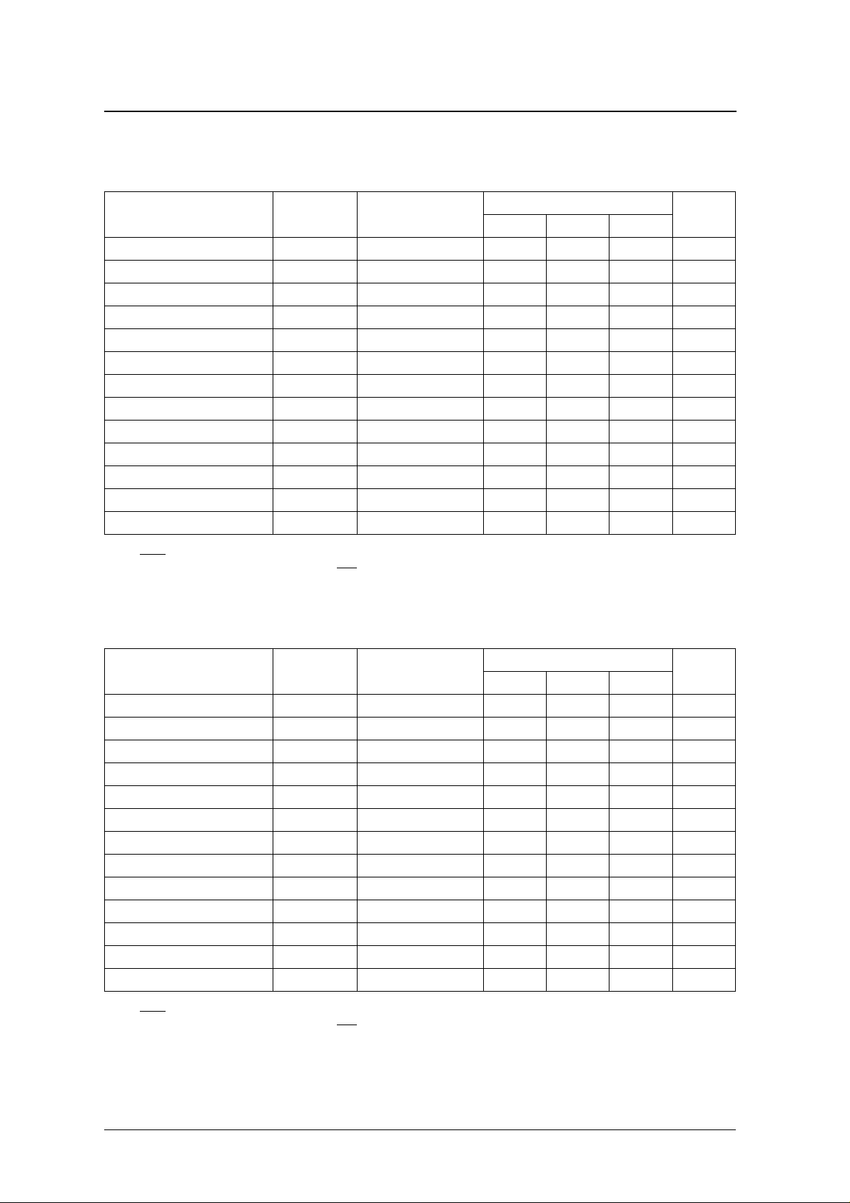
Filter Characteristics
8-times interpolation filter
SM5841H
Parameter
Passband attenuation
f @ fs = 44.1 kHz min typ max
– 0.20 –
0 to 0.4535fs 0 to 20 kHz
Passband ripple −0.03 – +0.03
0.5465fs to 3.4535fs 24.1 to 152 kHz 53 – –
Frequency Rating (dB)
Stopband attenuation
3.4535fs to 4.5465fs 152 to 201 kHz 50 – –
4.5465fs to 7.4535fs 201 to 328 kHz 53 – –
8fs filter response with deemphasis OFF
0
20
(dB)
40
60
Attenuation
80
100
120
0.0 1.0 2.0 3.0 4.0 5.0 6.0 7.0 8.0
Frequency
(fs)
8fs filter passband response with deemphasis OFF
-0.0001
-0.00005
(dB)
0.00000
0.00005
Attenuation
0.0001
0.000 0.125 0.250 0.375 0.500
Frequency
8fs filter band transition response with deemphasis OFF
0
10
20
(dB)
30
40
Attenuation
50
60
70
0.440 0.465 0.490 0.515 0.540 0.565 0.590 0.615 0.640
Frequency
(fs)
(fs)
NIPPON PRECISION CIRCUITS—9
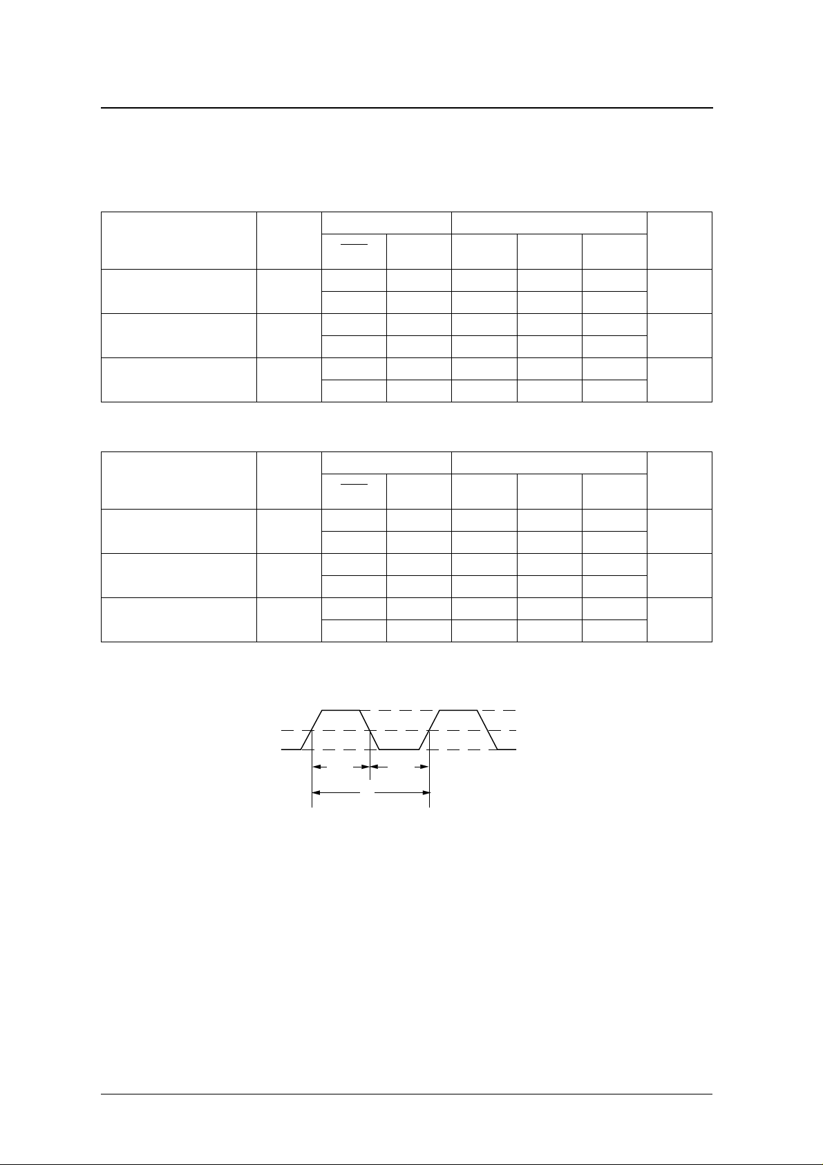
Deemphasis filter
SM5841H
Parameter
Passband bandwidth (kHz) 0 to 14.5 0 to 20.0 0 to 21.7
Attenuation (dB) −0.40 to +0.40 −0.05 to +0.15 −0.30 to +0.05
Deviation from ideal characteristic
1. The maximum deviation from an ideal filter with 0 dB attenuation and 0° phase characteristics for a 1 kHz input signal.
1
Phase, θ (°) −2 to 19 −1 to 15 −1 to 14
32 kHz 44.1 kHz 48 kHz
Sampling frequency
Passband response with deemphasis ON (fs = 44.1 kHz)
0
2
4
6
Attenuation (dB)
8
10
10 20 50 100 200 500 1k 2k 5k 10k 20k
Frequency (Hz)
Passband response with deemphasis ON (fs = 32/48 kHz)
0
2
4
6
Attenuation (dB)
8
10
10 20 50 100 200 500 1k 2k 5k 10k 20k
Frequency (Hz)
48kHz
32kHz
NIPPON PRECISION CIRCUITS—10

SM5841H
FUNCTIONAL DESCRIPTION
The basic arithmetic block is shown in figure 1, and
the function of each block is described in the following sections.
Input
fs
fs
Attenuator
fs
1st FIR
69th - order
2 × interpolator
Deemphasis IIR filter
fs
2fs
2nd FIR
13th - order
2 × interpolator
4fs
3rd FIR
9th - order
2 × interpolator
8fs
Output
Figure 1. Arithmetic block diagram
8-times Oversampling (Interpolation)
The interpolation arithmetic block is comprised of 3
cascaded, 2-times FIR interpolation filters, as shown
in figure 1.
The input signal is sampled at rate fs, and then 8times oversampling data is output. Sampling noise in
the 0.5465fs to 7.4535fs stopband is removed by the
interpolation filter.
Digital Deemphasis (DSF1, DSF2)
The digital deemphasis filter has the same construction as analog filters. It is implemented as an IIR filter to faithfully reproduce the gain and phase
characteristics of standard analog deemphasis filters.
The filter coefficients for fs = 32.0/44.1/48.0 kHz
sampling frequency are selected by DSF1 and DSF2
when the sampling frequency is specified, as shown
in the following table.
DSF1 DSF2 Deemphasis Sampling frequency
LOW L O W On 44.1 kHz
LOW HIGH On 48.0 kHz
HIGH LOW Off –
HIGH HIGH On 32.0 kHz
NIPPON PRECISION CIRCUITS—11
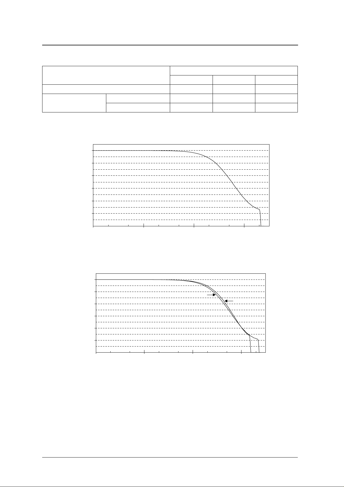
System Clock (CKI, CKO, CKSL)
SM5841H
Two system clock frequencies, 384fs and 256fs, can
be used. The clock is input on CKI. The CKI input
inverter has a feedback resistor to allow AC-coupled
input clocks. The system clock is also buffered and
then output on CKO. The system clock frequency
selection and the internal clock frequency are shown
in the following table.
CKSL
CKI
CKO
Figure 2. Clock generator circuit
Parameter
CKI input system clock frequency (f
CKO clock frequency 384fs 256fs
Internal clock frequency 128fs 128fs
Serial output clock frequency 192fs 256fs
) 384fs 256fs
SYS
CKSL
HIGH LOW
to timing controller
CKSL = H
1 / 3
Internal system clock
(128fs)
1 / 2
CKSL = L
to timing controller
Noise Shaper and I/O Data Length (WSL1, WSL2)
The SM5841H has functions that can be used to suppress the level of requantization noise due to the
inherent arithmetic rounding-off that occurs in digital signal processing.
■ 16/18-bit input
The input interface accepts 16 and 18-bit input
source data. That means that if 16-bit source data
is digitally processed, for example in a sound field
control or other DSP, the output can be input to the
SM5841H without the same need for roundingoff, thereby avoiding the requantization noise that
would otherwise occur.
■ 16/18/20-bit output
The output interface can support 18 and 20-bit
output data, making connection to 18 or 20-bit
D/A converters possible. As a result, the requantization noise generated after digital processing can
be greatly reduced.
■ Noise shaper function
The 1st-order noise shaper processing occurs on
the digital filter output. It reduces the requantization noise for 16 and 18-bit input signals to levels
inherent in 18 and 20-bit output modes, respectively. The noise shaper does no processing on 20bit output data.
There are 4 input data and output data length combinations possible, selected by the state of WSL1 and
WSL2 as shown in the following table.
WSL1 WSL2
HIGH HIGH Off 18 bits 20 bits
HIGH LOW On 18 bits 18 bits
LOW HIGH On 16 bits 18 bits
LOW LOW On 16 bits 16 bits
Noise
shaper
Input bit
length
Output bit
length
NIPPON PRECISION CIRCUITS—12

Audio Data Input (DIN, BCKI, LRCI)
SM5841H
The input data is in 16/18-bit serial, 2s complement,
MSB first format.
Serial input data on DIN is clocked into an SIPO
(serial in, parallel out) register on the rising edge of
the BCKI bit clock, and then converted to parallel
data.
SIPO output data is transferred into the left and
right-channel input registers on the falling edge and
rising edge, respectively, of the LRCI clock.
Lch
MSB
16 / 18bit
DIN
BCKI
LRCI
Figure 3. Audio data input timing
The internal arithmetic operation and output circuit
timing is independent of the input timing. Accordingly, phase differences between LRCI, BCKI and
CKI do not affect device operation, and any jitter in
the data input clock does not cause jitter in the output
clock.
Note that the device should be reset if either or both
of the LRCI and CKI clocks stop. If the device is not
reset, even though the clocks are low frequency,
incorrect circuit operation may occur, generating
unwanted output noise.
1/fs
LSB
Rch
MSB
16 / 18bit
LSB
NIPPON PRECISION CIRCUITS—13

SM5841H
Audio Data Output (DOL, DOR, BCKO, WCKO, OFST)
The output data is in 16/18/20-bit serial, 8fs, simultaneous left and right-channel, 2s complement, MSB
first format.
A DC offset can be added to arithmetic data before
the data is output to reduce the D/A converter zerocrossing distortion for very small input signals. The
offset added is approximately 0.8% of full-scale for
the corresponding output bit length, as shown below.
■ 512 LSB for 16-bit output
■ 2048 LSB for 18-bit output
■ 8192 LSB for 20-bit output
The DC offset is added to the output when OFST is
HIGH. DC offset is OFF when OFST is LOW.
System Clock
BCKO
DOL or DOR
TB
12 435
WCKO
6TB
8fs serial data is output on independent DOL and
DOR channels, in sync with the falling edge of the
internal system clock and BCKO clock. The number
of BCKO bit clock pulses per word changes depending on the output bit length selected (16/18/20 bits).
Consequently, output data is latched into the D/A
converter internal register on the falling of the edge
of an output word clock WCKO, which has timing
independent of the number of output bits as specified
in the following table.
Parameter Symbol CKSL = HIGH CKSL = LOW
Bit clock rate T
Data word length T
11 12 1413 15 16 17 1918 20
18TB
DW = 24TB
T
DW
t
B
(1/192fs) t
SYS
24T
B
12 43
SYS
(1/256fs)
32T
B
The number of output bits is determined by the output bit length selected.
Figure 4. 8fs data output timing (CKSL = HIGH)
System Clock
BCKO
DOL or DOR
TB
12 435
WCKO
6TB
The number of output bits is determined by the output bit length selected.
Figure 5. 8fs data output timing (CKSL = LOW)
11 12 1413 15 16 17 1918 20
26TB
T
DW = 32TB
12 43
NIPPON PRECISION CIRCUITS—14

System Reset and Output Muting (RST)
SM5841H
System reset
The SM5841H must be reset at power-ON by applying a LOW-level pulse on RST.
At system reset, the arithmetic and output timing
counters are reset on the next LRCI start edge, as
long as the CKI clock has already stabilized.
The power-ON reset pulse can be applied by a
microcontroller or, for systems where CKI and LRCI
are stable at power-ON, by connecting a 300 pF
capacitor between RST
and VSS. For systems that do
not use a microcontroller, the capacitor must be chosen such that the CKI and LRCI clocks fully stabilize
before RST goes from LOW to HIGH.
RST
LRCI
Internal reset
DOL
DOR
(L)
1234
(L)
If the system clock is interrupted or is corrupted by
jitter, after power-ON reset and all internal timing is
synchronized, such that a timing error greater than
±3/8 × f
occurs, the internal timing is automati-
LRCI
cally reset on the next LRCI start edge. This resynchronization affects the internal operation and can
generate a momentary click noise output.
Output muting
When RST goes LOW, the DOL and DOR outputs
go LOW, immediately muting the output signal, and
they remain LOW for interv als in w ord units. Muting
is released and timing is synchronized on the 3rd rising edge of LRCI after RST
goes HIGH. Note that
during muted output, the BCKO and WCKO clocks
do not stop.
Figure 6. System reset timing and output muting
NIPPON PRECISION CIRCUITS—15

SM5841H
TIMING DIAGRAMS
Input Timing Examples (DIN, BCKI, LRCI)
(MSB) (LSB)
18bit Lch
DIN
BCKI
(MSB) (LSB)
18bit Rch
Audio
ICs
LRCI
DIN
BCKI
LRCI
1 / fs
Figure 7. 18-bit input timing
(MSB) (LSB)
16bit Lch
1 / fs
Figure 8. 16-bit input timing
(MSB)
16bit Rch
(LSB)
NIPPON PRECISION CIRCUITS—16

SM5841H
Output Timing Examples (DOL, DOR, BCKO, WCKO)
System Clock
BCKO
TB
DOL or DOR
12 435
WCKO
6TB
The number of output bits is determined by the output bit length selected.
Figure 9. 8fs data output timing (CKSL = HIGH)
System Clock
BCKO
DOL or DOR
TB
12 435
WCKO
6TB
The number of output bits is determined by the output bit length selected.
Figure 10. 8fs data output timing (CKSL = LOW)
11 12 1413 15 16 17 1918 20
18TB
T
DW = 24TB
11 12 1413 15 16 17 1918 20
26TB
DW = 32TB
T
12 43
12 43
NIPPON PRECISION CIRCUITS—17

APPLICATION CIRCUITS
Input Interface Circuits
SM5841H
SONY
CXD2500
PSSL
MATSUSHITA
MN6617
SEL
IPSEL
YAMAHA
YM3623
C16M
LRDK
DA16
DA15
XCK
R / L
SRDATA
SRCK
OA
L / R
DO
BCO
16.9344MHz
44.1kHz
2.1168MHz
16.9344MHz
44.1kHz
2.1168MHz
16.9344MHz
44.1kHz
2.1168MHz
CKI
LRCI
DIN
BCKI
CKI
LRCI
DIN
BCKI
CKI
LRCI
DIN
BCKI
CKSL
SM5841H
WSL1
CKSL
SM5841H
WSL1
CKSL
SM5841H
WSL1
TOSHIBA
TC9200F
17MO
CHCK
DOUT
BCK
16.9344MHz
44.1kHz
2.1168MHz
CKI
LRCI
DIN
BCKI
CKSL
SM5841H
WSL1
NIPPON PRECISION CIRCUITS—18

Output Interface Circuits
18-bit, 2-DAC (8fs L+R output mode)
SM5841H
CLOCK
L. E.
DATA
CLOCK
SM5841H
(16bit Input)
WCKO
DOL
DOR
BCKO
L. E.
WSL1
This example is for 16-bit input mode, so WSL1 is tied HIGH. For 18-bit mode, WSL1 is tied LOW.
DATA
BURR - BROWN
PCM58P
BURR - BROWN
PCM58P
16-bit, 1-DAC (8fs L+R output mode)
SM5841H
(16bit Input)
WSL1
WSL2
WCKO
DOL
DOR
BCKO
WCKO
LSI
RSI
CLK
NEC
µPD6376
4/8fs SEL
Lch OutPut
Rch OutPut
Lch Output
Rch Output
NIPPON PRECISION CIRCUITS—19

SM5841H
NIPPON PRECISION CIRCUITS INC. reserves the right to make changes to the products described in this data sheet in order to
improve the design or performance and to supply the best possible products. Nippon Precision Circuits Inc. assumes no responsibility for
the use of any circuits shown in this data sheet, conveys no license under any patent or other rights, and makes no claim that the circuits
are free from patent infringement. Applications for any devices shown in this data sheet are for illustration only and Nippon Precision
Circuits Inc. makes no claim or warr anty that such applications will be suitab le for the use specified without further testing or modification.
The products described in this data sheet are not intended to use for the apparatus which influence human lives due to the failure or
malfunction of the products. Customers are requested to comply with applicable laws and regulations in effect now and hereinafter,
including compliance with export controls on the distribution or dissemination of the products. Customers shall not expor t, directly or
indirectly, any products without first obtaining required licenses and approvals from appropriate government agencies.
NIPPON PRECISION CIRCUITS INC.
4-3, Fukuzumi 2-chome
Koto-ku, Tokyo 135-8430, Japan
NIPPON PRECISION CIRCUITS INC.
Telephone: 03-3642-6661
Facsimile: 03-3642-6698
NC9625AE 1998.06
NIPPON PRECISION CIRCUITS—20
 Loading...