

SM5158A
Serial input PLL frequency synthesizer
NIPPON PRECISION CIRCUITS-1
NIPPON PRECISION CIRCUITS INC.
OVERVIEW
The SM5158A is a serial data programmable PLL Frequency Synthesizer LSI fabricated
in NPC's proprietary Molybdenum-gate
CMOS technology.
Ratios of reference frequency divider and
input frequency divider can be independently
set.
FEATURES
- Up to 200MHz input frequency
(VDD=4.5V)
- Up to 35MHz reference frequency
(VDD=4.5V)
- 5 to 65535 programmable reference
frequency divider ratio
- 1056 to 65535 programmable input
frequency divider ratio
- Lock detector
- Either Active or Passive filter can be
externally used.
- 16-pin plastic DIP and 16-pin S-SOP
- Molybdenum gate CMOS structure
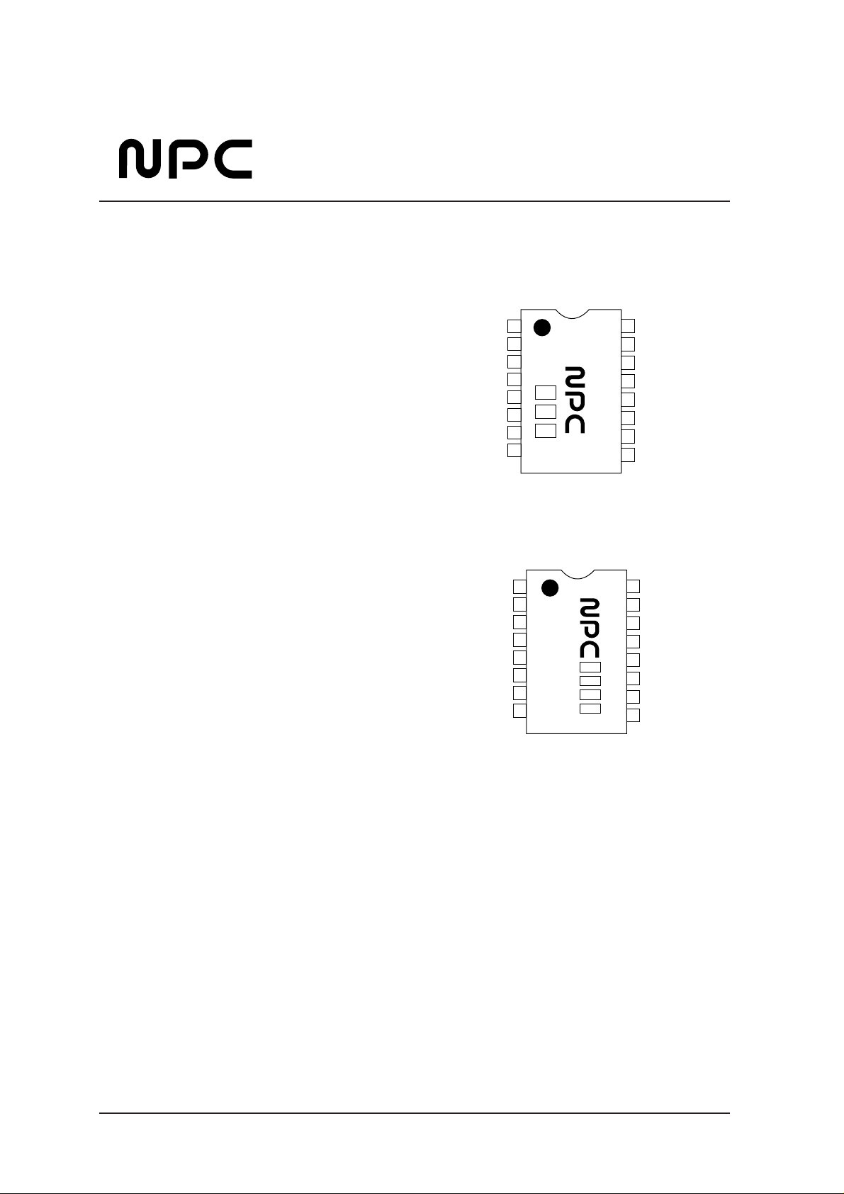
PIN OUT
16-pin SSOP
16-pin DIP
158A
OR
OV
TEST
FR
DOA
LE
DATA
CLK
XIN
XOUT
FV
VDD
DOP
VSS
LD
FIN
1
8
9
16
SM158AP
OR
OV
TEST
FR
DOA
LE
DATA
CLK
XIN
XOUT
FV
VDD
DOP
VSS
LD
FIN
1
8
9
16
NIPPON PRECISION CIRCUITS-2
SM5158AS
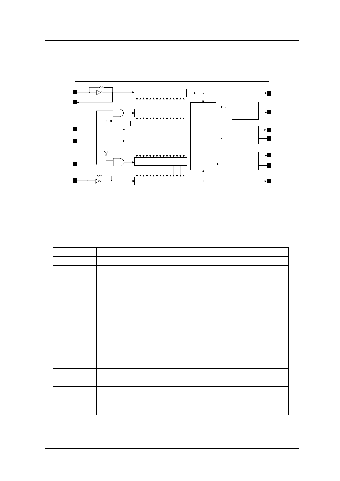
BLOCK DIAGRAM
PIN DESCRIPTION
16 BIT COUNTER
PHASE
DETECTOR
LOCK
DETECTOR
CHARGE
PUMP
16 BIT N COUNTER
FIN
DATA
LD
FV
XOUT
LE
CLK
FR
DOA
DOP
OV
OR
16 BIT LATCH
BUFFER
16 BIT LATCH
17 BIT SHIFT REGISTER
XIN
Number Name Description
1 XIN To connect external crystal and capacitor, or external clock input pin.
2 XOUT To connect external crystal and capacitor,or oscilator output signal can be available at this pin.
3 FV Buffered input frequency divider output.phase detector input
4 VDD Positive supply pin. Apply +2.7 to 5.5 Volts.
5 DOP Charge pump output for passive lowpass filter. Single ended tristate output.
6 VSS Ground.
7 LD Lock detector output. Logic Low when PLL is unlocked.
8 FIN Comparison frequency input.Internal feedback resistor for AC coupling.
Input frequency range 20MHz to 200MHz.
9 CLK Shift register clock input.
10 DATA Serial data input.
11 LE Latch enable input.
12 DOA Chrage pump output for active lowpass filter. Single ended tristate output.
13 FR Buffered reference frequency devider output. Phase detector input.
14 TEST Test pin. Left open.
15 OV Buffered phase detector output to a differential lowpass filter.
16 OR Buffered phase detector output to a differential lowpass filter.
NIPPON PRECISION CIRCUITS-3
SM5158A
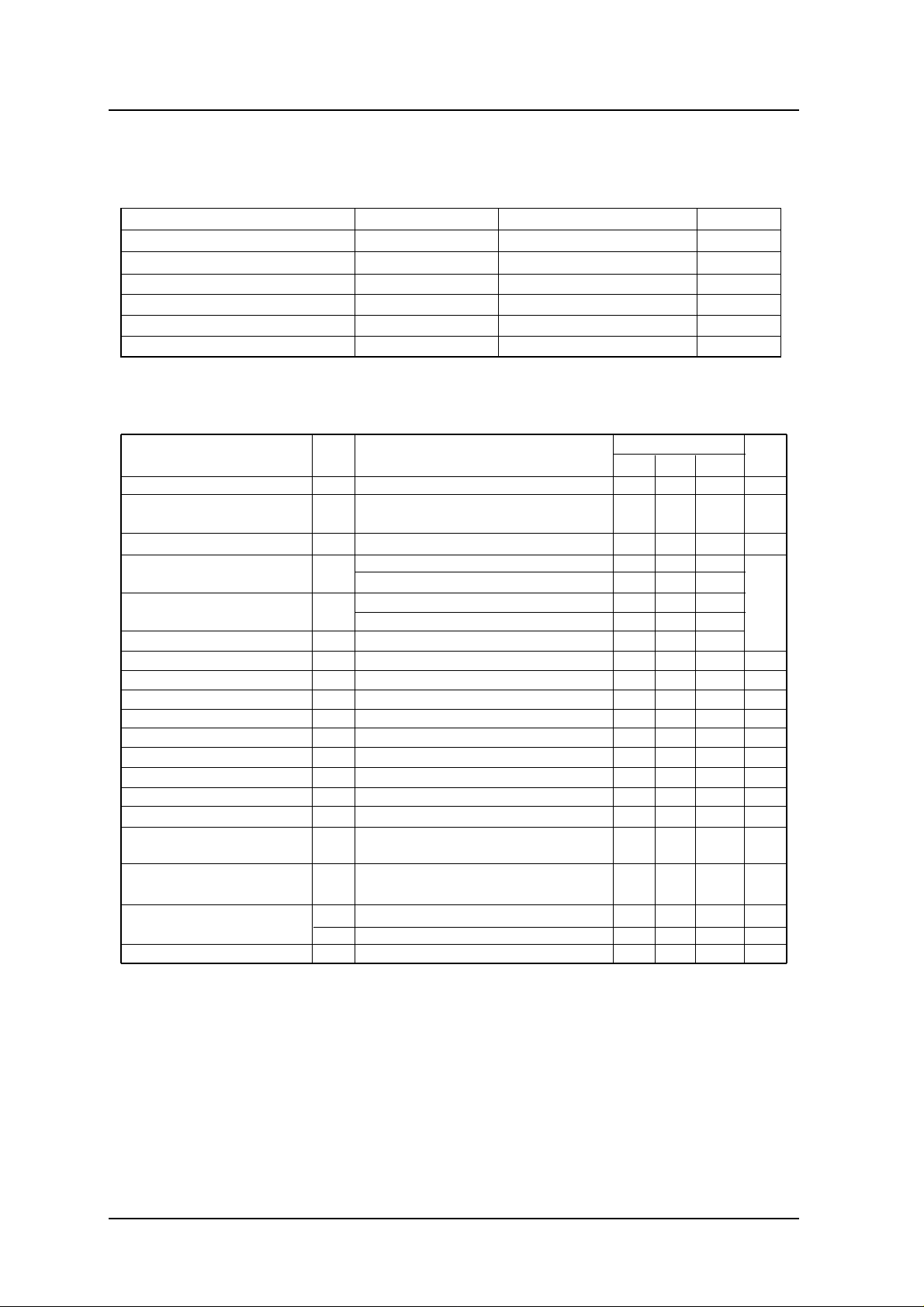
SPECIFICATION
Absolute Maximum Ratings
Electrical Characteristics
Parameter Symbol Rating Unit
Supply voltage range VDD - VSS -0.3 to 7.0 V
Input voltage range VIN VSS-0.3 to VDD+0.3 V
Operating temperature range TOPR -30 to +85 deg.C
Storange temperature Tstg -40 to 125 deg.C
Solding temperature Tsld 255 deg.C
Solding time tsld 10 S
Rating
Parameter Symbol Condition min typ max Unit
Supply Voltage VDD 2.7 5.5 V
Supply current in operating mode IDD FIN 200MHz , VFIN=0.5Vp-p sine wave 10 23.5 mA
XIN=20MHz, VFIN=0.5Vp-p sine wave
Supply current in stanby mode IDD2 R/N latch's all bits="0" - - 10 uA
FIN maximum operating frequency fmax1 FIN=0.5Vp-p , sine wave (VDD=2.7V) 100 120
FIN=0.5Vp-p , sine wave (VDD=4.5V) 200 240
XIN maximum operating frequency fmax2 XIN=0.5Vp-p , sine wave(VDD=2.7V) 20 MHz
XIN=0.5Vp-p , sine wave(VDD=4.5V) 35
FIN minimum operating frequency fmin1 FIN=0.5Vp-p , sine wave 20
XIN minimum operating frequency fmin2 FIN=0.5Vp-p , sine wave 1
FIN input voltage VFIN fFIN = 20 to 200MHz sine wave , AC coupling 0.5 VDD-0.5 Vp-p
XIN input voltage VXIN fXIN = 1 to 35MHz sine wave , AC coupling 0.5 VDD-0.5 Vp-p
CLK, DATA, LE HIGH-level input voltage VIH VDD-0.3 uA
CLK, DATA, LE LOW-level input voltage VIL 0.3 uA
FIN HIGH-level input current IIH1 VIH=VDD 100 uA
FIN LOW-level input current IIL1 VIL=0V 100 uA
XIN HIGH-level input current IIH2 VIH=VDD 100 uA
XIN LOW-level input current IIL2 VIL=0V 100 uA
FV, DOP, LD,DOA, FR, OV, OR, IOH VOH=VDD-0.4V 0.4 mA
HIGH-level output current
FV, DOP, LD,DOA, FR, OV, OR, IOL VOL=0.4V 0.4 mA
LOW-level output current
DATA to CLK and CLK to LE tsu1 80 ns
setup time tsu2 80 ns
Hold time tH 80 ns

NIPPON PRECISION CIRCUITS-4
SM5158A
Serial data input timing
Phase detector timing
DATA
CLK
LE
tSU1
tH
tSU2
FR
FV
DOP
OR
DOA
OV
LD

DIVIDER DATA SETTING PROCEDURE
NIPPON PRECISION CIRCUITS-5
SM5158A
CLK
DATA
LE
12 34567 8 9101112131415 1716
MSB LSB
Control
Input data must be MSB first. Final bit(17th
bit) is assigned to the control bit.
Data are written into shift register at the rising edge of the CLK signal.
When LE is HIGH,data is transferred from
the shift register to either the latch of reference divider or input divider. Thus data must
be written on the shift register while LE is
remaining LOW.
While all bits of the N latch to are "0", the N
counter will be disabled, DOA, DOP are
floating,and the supply current will be
decreased.
While all bits of the R latch are "O", oscillator will be disabled.
While all bits of R and N latches are "0", supply current decreases to 10uA or less.
CONTROL
LSB
MSB
16 BIT DATA FOR R or N latch
Latch select bit ( 1 : R-latch, 0 : N-latch )

NIPPON PRECISION CIRCUITS-6
SM5158A
LOW PASS FILTERS
DOP
DOA
OR
OV
VCO
R1
R2
C
DOP
DOA
OR
OV
VCO
DOP
DOA
OR
OV
VCO
VDDVDD
C
RL
R2
R1
510KΩ
R1
R1
R2
C
+
R2
C
b. Active filter
a. Passive filter
c. Differential filter

NIPPON PRECISION CIRCUITS INC. reserves the right to make changes to the products described in this data sheet
in order to improve the design or performance and to supply the best possible products. Nippon Precision Circuits Inc.
assumes no responsibility for the use of any circuits shown in this data sheet, conveys no license under any patent or other
rights, and makes no claim that the circuits are free from patent infringement. Applications for any devices shown in this data
sheet are for illustration only and Nippon Precision Circuits Inc. makes no claim or warranty that such applications will be
suitable for the use specified without further testing or modification. The products described in this data sheet are not intended
to use for the apparatus which influence human lives due to the failure or malfunction of the products. Customers are requested to comply with applicable laws and regulations in effect now and hereinafter, including compliance with export controls on
the distribution or dissemination of the products. Customers shall not export, directly or indirectly, any products without first
obtaining required licenses and approvals from appropriate government agencies.
NIPPON PRECISION CIRCUITS-7
SM5158A
NC9306BE 1998 1
NIPPON PRECISION CIRCUITS INC.
4-3, 2-chome Fukuzumi, Koto-ku
Tokyo, 135 -8430, JAPAN
Telephon: 03-3642-6661
Facsimile: 03-3642-6698
PACKAGE DIMENSIONS
UNIT:mm
16pin SSOP
16pin DIP
0.6TYP
6.8 0.3
0.80.36 0.1
0.4 0.2
010
0.15
+ 0.10
- 0.05
0.05 0.05
1.5 0.1
4.4 0.2
6.2 0.3
2.54
0.5 0.1
1.5
+ 0.30
- 0.05
3.4 0.1
4.0 0.33.3 0.2
6.5 0.2
7.62
0.3
+ 0.10
- 0.05
0 to 15˚
19.5 0.3
0.86 typ.
NIPPON PRECISION CIRCUITS INC.
 Loading...