


SM5013 series
NIPPON PRECISION CIRCUITS—1
NIPPON PRECISION CIRCUITS INC.
Quartz Crystal Oscillator IC
OVERVIEW
The SM5013 Series crystal oscillator module ICs
fabricated in NPC’s Molybdenum-gate CMOS. They
comprise low-voltage low-current consumption
oscillator circuits and output buffers. They incorporate built-in oscillation capacitance with superior frequency response to realize.
FEATURES
■
4.5 to 5.5 V supply voltage
■
Oscillation capacitances built-in (CG and CD)
■
Output drive capability : 8 mA (V
DD
=
4.5V)
■
Output duty level
• SM5013KDH : CMOS
• SM5013LDH : TTL
■
3rd overtone oscillation
■
Output frequency : fo (Oscillation frequency)
■
Input level : TTL
■
3 state function
■
6 pin SOT (SM5013×DH)
■
Chip form (CF5013×D)
ORDERING INFOMATION
Device Package
SM5013×DH 6pinSOT
CF5013×D Chip form
SM5013 series
NIPPON PRECISION CIRCUITS—2
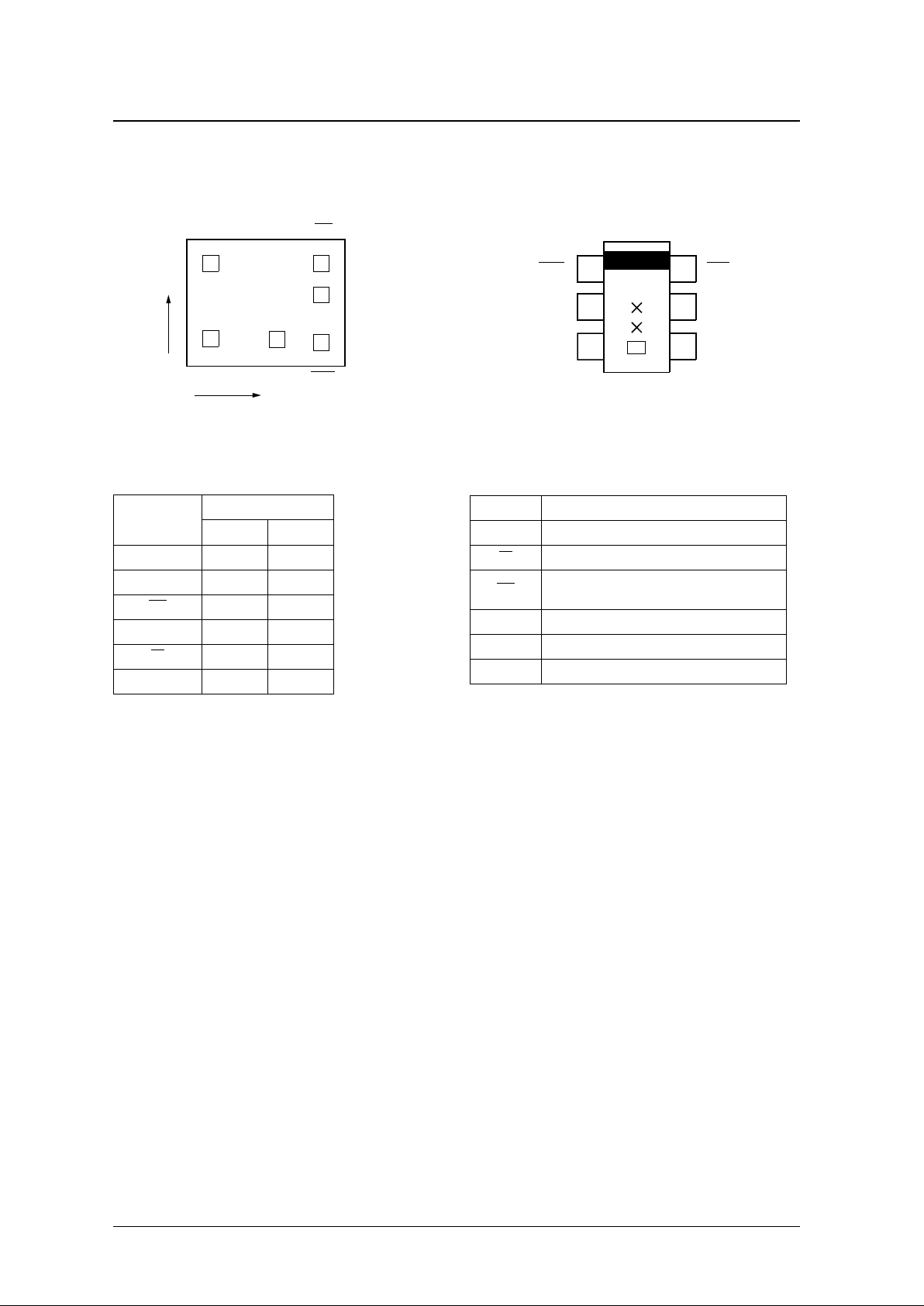
PAD DIMENSIONS
( UNIT : µm )
PAD COORDINATES
Chip size : 1.00 × 0.80mm
Chip thickness : 250 ± 30µm
Chip reverse side : VDD level
PIN OUT
( Top View )
PIN DESCRIPTIONS
Pad
Coordinate(µm)
XY
VSS 150 174
XT 570 170
INH 850 150
VDD 850 450
XT 850 650
Q 150 650
Q
XT
(1000,800)
VDD
INH
XTVSS
(0,0)
X
Y
PIN DESCRIPTION
XT Oscillator input pin
XT Oscillator output pin
INH
Output state control input pin ( with built-in pull-up
resistance
VDD Supply voltage
VSS Ground
Q Output pin ( fo : Oscillator frequency)
1INH
2XT
VSS
4Q
5 VDD
6XT
3
3
SM5013 series
NIPPON PRECISION CIRCUITS—3
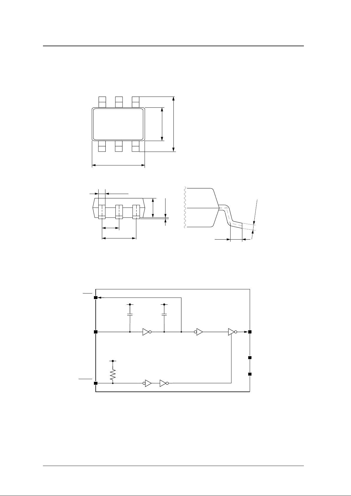
PACKAGE DIMENSIONS
(UNIT : mm)
• 6pin SOT
BLOCK DIAGRAM
2.9 ± 0.2
0.95
0.40 ± 0.1
1.60
1.1 ± 0.1
+ 0.2
− 0.1
2.8
+ 0.2
− 0.3
0.45
0 to 0.15
1.9 ± 0.2
0.15
+ 0.1
− 0.05
XT
XT
INH
VSS
VDD
Q
CG CD

SM5013 series
NIPPON PRECISION CIRCUITS—4
DEVICE LIST
Note that the operating frequency is highly dependent on the frequency of the crystal used.
Current consumption and Output waveform with NPC’s standard crystal
Device
Target frequency range
(MHz)
gm (relative value) Output (stand by)
Internal capacitance
C
G
(pf) CD(pf)
CF5013KD 22 to 70 CMOS Hi − Z 8 15
CF5013LD 22 to 70 TTL Hi − Z 8 15
f (MHz) R (Ω) L (mH) Ca (fF) Cb (pF)
30 18.62 16.24 1.733 5.337
40 20.53 11.34 1.396 3.989
50 22.17 7.40 1.370 4.105
60 22.20 5.05 1.388 4.226
70 25.42 4.18 1.254 5.170
L
Ca R
Cb

SM5013 series
NIPPON PRECISION CIRCUITS—5
SPECIFICATIONS
Absolute Maximum Ratings
VSS = 0V, unless otherwise noted.
Recommended Operating Conditions
VSS = 0V, unless otherwise noted.
Electrical Characteristics
VDD = 4.5 to 5.5V, VSS = 0V, Ta = − 20 to 80 °C, unless otherwise noted.
Parameter Symbol Condition Rating unit
Supply voltage range V
DD
−
0.5 to + 7.0 V
Input voltage range V
IN
−
0.5 to VDD + 0.5 V
Output voltage range V
OUT
−
0.5 to VDD + 0.5 V
Operating temperature range T
opr
−
40 to + 85
°
C
Standard temperature range T
STG
SOT6
−
55 to + 125
°
C
Chip form
−
65 to + 150
°
C
Output current I
OUT
13 mA
Power dissipation P
W
SOT6 250 mW
Soldering temperature T
SLD
SOT6 255
°
C
Soldering time t
SLD
SOT6 10 s
Parameter Symbol Condition
Limit
unit
min typ max
Supply Voltage V
DD
4.5
−
5.5 V
Input voltage V
IN
V
SS
−
V
DD
V
Operating temperature T
OPR
−
20
−+
80
°
C
Parameter Symbol Condition
Limit
unit
min typ max
HIGH - level output voltage V
OH
Q pin, test circuit 1, VDD = 4.5V, IOH = 8mA 3.9 4.2
−
V
LOW - level output voltage V
OL
Q pin, test circuit 2, VDD = 4.5V, IOL = 8mA
−
0.3 0.4 V
Output leakage current I
Z
Q pin, test circuit 2, INH = Low,
VDD = 5.5V
V
OH
= V
DD
−−
10
µ
A
VOL = V
SS
−−
10
µ
A
HIGH - level input voltage V
IH
INH pin 2.0
−−
V
LOW - level input voltage VILINH pin
−−
0.8 V
Current consumption I
DD
INH = OPEN, test circuit 3,
C
L
= 15pF, f = 70MHz
CF5013KD, load circuit 1
−
28 45 mA
CF5013LD, load circuit 2
−
28 45 mA
Pull - up resistance R
UP
INH pin, test circuit 4 25 100 250 k
Ω
Internal capacitance
C
G
Design value, determined by the internal wafer pattern
7.2 8 8.8 pF
C
D
13.5 15 16.5 pF

SM5013 series
NIPPON PRECISION CIRCUITS—6
Switching Characteristics
CF5013KD (Duty level CMOS )
VDD = 4.5 to 5.5V, VSS = 0V, Ta = − 20 to 80 °C, unless otherwise noted.
CF5013LD (Duty level TTL )
VDD = 4.5 to 5.5V, VSS = 0V, Ta = − 20 to 80 °C, unless otherwise noted.
FUNCTIONAL DESCRIPTION
Stand − by Function
When INH pin is Low-level, Q pin will be high-impedance.
Parameter Symbol Condition
Limit
unit
min typ max
Output rise time trTest circuit 5, load circuit 1, CL = 15pF, 0.1VDD → 0.9V
DD
− 3.5 7 ns
Output fall time tfTest circuit 5, load circuit 1, CL = 15pF, 0.9VDD → 0.1V
DD
− 3.5 7 ns
Output duty cycle
1
1. Determined by the lot monitor.
DUTY
Test circuit 5, Ta = 25°C, V
DD
= 5.0V
load circuit 1, CL = 15pF, f = 70MHz
45 − 55 %
Output disable delay time t
PLZ
Test circuit 5, Ta = 25°C, VDD = 5.0V, load circuit 1, CL = 15pF
−−100 ns
Output enable delay time t
PZL
−−100 ns
Parameter Symbol Condition
Limit
unit
min typ max
Output rise time trTest circuit 5, load circuit 2, CL = 15pF, 0.4V → 2.4V − 2.5 7 ns
Output fall time tfTest circuit 5, load circuit 2, CL = 15pF, 2.4V → 0.4V − 2.5 7 ns
Output duty cycle
1
1. Determined by the lot monitor.
DUTY
Test circuit 5, Ta = 25°C, VDD = 5.0V
load circuit 2, CL = 15pF, f = 70MHz
45 − 55 %
Output disable delay time t
PLZ
Test circuit 5, Ta = 25°C, VDD = 5.0V, load circuit 2, CL = 15pF
−−100 ns
Output enable delay time t
PZL
−−100 ns
INH Q
High(open) Output
Low Hi - Z

SM5013 series
NIPPON PRECISION CIRCUITS—7
TEST CIRCUITS
Test Circuit 1
3.5 V
P − P
, 10MHz sine wave input signal
Test Circuit 2
Test Circuit 3
3.5 V
P − P
, 70MHz sine wave input signal
Test Circuit 4
Test Circuit 5
X’tal = 70MHz
Rfo = 2.7kΩ
Signal
Generator
VDD
VSS
XT Q
R1 R2
C1
C1: 0.001µF
R1: 50
Ω
R2: 490 Ω
R3: 100 kΩ
VOH
0V
Q out monitor
XT
R3
VDD
VSS
Q
A
V
IOL, IZ
IZ
VOL
INH
Signal
Generator
VDD
VSS
XT Q
R1
I
DD
C1
C1: 0.001 µF
R1: 50
Ω
R3: 100 kΩ
A
XT
R3
VDD
VSS
INH
IPR
RUP=
V
DD
IPR
A
VDD
VSS
XT
XT
Rfo
Q
X'tal
INH

SM5013 series
NIPPON PRECISION CIRCUITS—8
Load Circuit 1 Load Circuit 2
Q output
CL=15pF(Including
probe capacity)
CL
Q output
VDD
C
L
CL=15pF(Including
proove capacity)
R=800Ω
R

SM5013 series
NIPPON PRECISION CIRCUITS—9
Switching Time T est Waveforms
(1) SM5013KD (Duty level CMOS)
• t
r
, tf , DUTY
• Output duty cycle time
(2) CF5013LD (Duty level TTL)
• t
r
, tf , DUTY
• Output duty cycle time
0.9VDD
0.1VDD
0.9VDD
0.1VDD
tr tf
Q output
DUTY measuring
voltage (0.5V
DD)
DUTY measuring
voltage
(0.5VDD)
Q output
TW
T
DUTY= (T
W/ T) 100 (%)
2.4V
0.4V
2.4V
0.4V
tr
tf
Q output
DUTY measuring
voltage (1.4V)
DUTY measuring
voltage
(1.4V)
Q output
TW
T
DUTY= (T
W/ T) 100 (%)

SM5013 series
NIPPON PRECISION CIRCUITS—10
NIPPON PRECISION CIRCUITS INC. reserves the right to make changes to the products described in this data sheet in order to
improve the design or performance and to supply the best possible products. Nippon Precision Circuits Inc. assumes no responsibility for
the use of any circuits shown in this data sheet, conveys no license under any patent or other rights, and makes no claim that the circuits
are free from patent infringement. Applications for any devices shown in this data sheet are for illustration only and Nippon Precision
Circuits Inc. makes no claim or warr anty that such applications will be suitab le for the use specified without further testing or modification.
The products described in this data sheet are not intended to use for the apparatus which influence human lives due to the failure or
malfunction of the products. Customers are requested to comply with applicable laws and regulations in effect now and hereinafter,
including compliance with export controls on the distribution or dissemination of the products. Customers shall not expor t, directly or
indirectly, any products without first obtaining required licenses and approvals from appropriate government agencies.
NIPPON PRECISION CIRCUITS INC.
4-3, 2-chome Fukuzumi
Koto-ku, Tokyo 135-8430, Japan
Telephone: 03-3642-6661
Facsimile: 03-3642-6698
NC9621CE 1998.08
NIPPON PRECISION CIRCUITS INC.
• Output Disable/Enable Delay Times
Q output
INH
VIH
VIL
tPLZ
tPZL
INH inputwaveform tr = tf 10ns
 Loading...