

Page 1
=
=
/8
查询CF5009AH1供应商查询CF5009AH1供应商
SM5009 series
Crystal Oscillator Module ICs
OVERVIEW
The SM5009 series are crystal oscillator module ICs that incorporate low crystal current type oscillating circuit
to limit oscillator-stage current, so that they can reduce crystal current lower than the existing products. Since
the oscillating circuit has oscillator capacitors with excellent frequency response and feedback resistor built-in,
just connecting crystal realizes stable fundamental oscillation responding up to 40MHz. The SM5009 series
are ideal for SMD type crystal oscillator using a strip-shaped crystal blank.
FEATURES
■
Low crystal current oscillator
Up to 40MHz operating frequency range (funda-
■
mental oscillation)
■
Operating supply voltage range
• 3V operation: 2.7 to 3.6V
• 5V operation: 4.5 to 5.5V
■
–40 to 85 ° C operating temperature range
■
Oscillation capacitors C
Inverter amplifier feedback resistor built-in
■
■
Standby function
G
, C
built-in
D
• Oscillator stops (AL series), high impedance in
standby mode
■
Low standby current
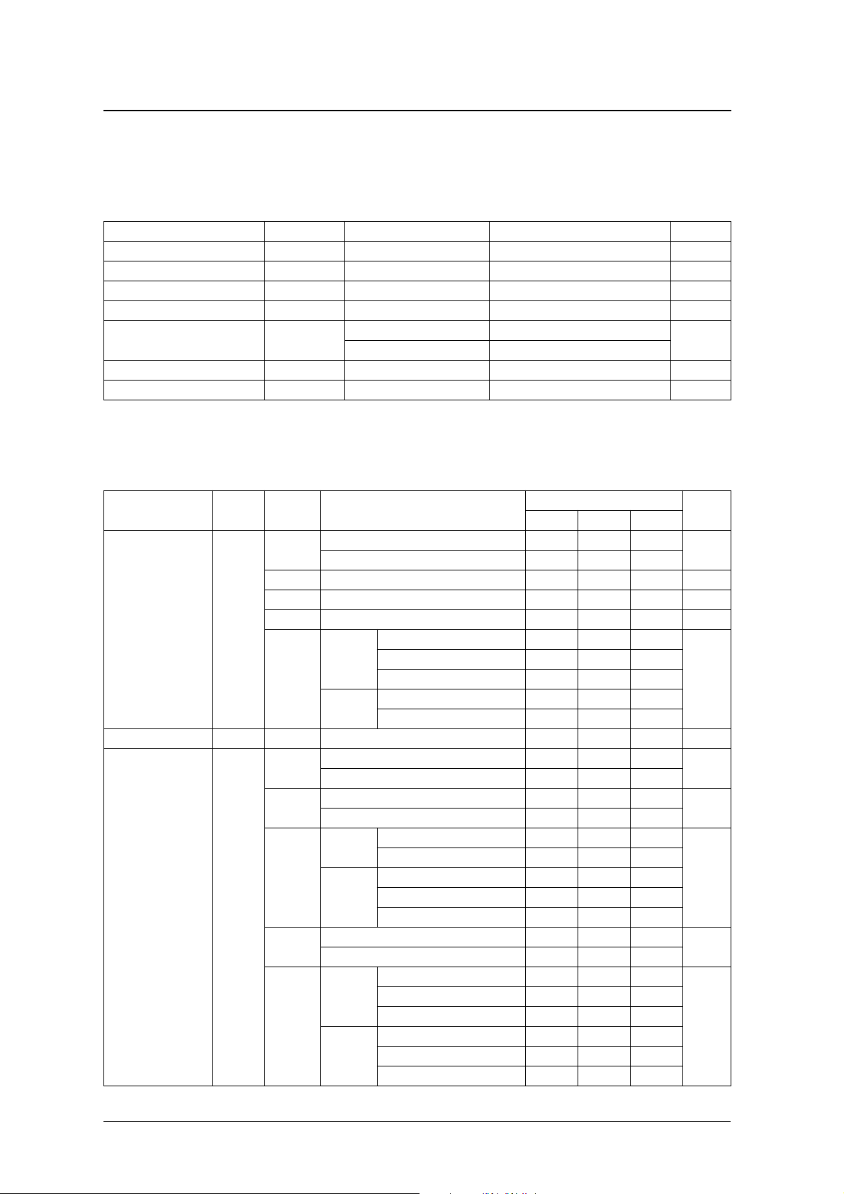
SERIES CONFIGURATION
3V operation 5V operation
Recommended
1
Version
CF5009AL1
CF5009AL2 f
CF5009AL3 f
CF5009AL4 f
CF5009AL5 f
CF5009AL6 f
CF5009AN1
CF5009AN2 f
CF5009AN3
CF5009AN4 f
CF5009AN5 f
CF5009AN6 f
CF5009CN1
CF5009CN2 f
CF5009AK1
CF5009AK2 f
CF5009AH1
CF5009AH2 f
CF5009AH3 f
CF5009AH4 f
1. Package devices (8-pin SOP) have designation SM5009 ××× S.
2. The recommended operating frequency is a yardstick value derived from the crystal used for NPC characteristics authentication. However, the oscillator frequency band is not guaranteed. Specifically, the characteristics can vary greatly due to crystal characteristics and mounting conditions, so
the oscillation characteristics of components must be carefully evaluated.
3. Output load value is the maximum load capacitance that allows drive.
operating
frequency
2
[MHz]
range
Up to 40 50 Up to 40 50 CMOS
Up to 40 30 Up to 40 50
Up to 30 15 Up to 30 50 CMOS
– – Up to 40 15 TTL
Up to 16 15 Up to 30 15 CMOS
Output
load
3
(max)
[pF]
Recommended
operating
frequency
2
range
[MHz]
Output
load
• Power-save pull-up resistor built-in (AL series)
Frequency divider built-in (f
■
f
/16, f
O
■
Output drive capability
/32 determined by internal connection)
O
, f
O
O
•AL × , AN × , AK × , CN × : 16mA (V
•AH × : 4mA (V
■
Output load: C
■
Output duty level
4.5V)
DD
= 50pF max.
L
• CMOS level (1/2 VDD): AL × , AN × , AH × , CN ×
• TTL level (1.4V): AK ×
■
Molybdenum-gate CMOS process
8-pin SOP (SM5009 ××× S)
■
■
Chip form (CF5009 ××× )
Standby mode
3
(max)
[pF]
Output
duty level
CMOS
CMOS/TTL
Output
frequency
f
O
/2
O
/4
O
/8
O
/16
O
/32
O
f
O
/2
O
f
/4
O
/8
O
/16
O
/32
O
f
O
/2
O
f
O
/2
O
f
O
/2
O
/4
O
O
Input
INH
level
CMOS Yes Hi-Z
TTL No Hi-Z
TTL No Hi-Z
TTL No Hi-Z
TTL No Hi-Z
Oscillator
stop
function
/2, f
DD
/4, f
O
4.5V)
Output
state
/8,
O
APPLICATIONS
■
SMD type crystal oscillator module
ORDERING INFORMATION
Device Package
SM5009 ××× S 8-pin SOP
CF5009 ××× –1 Chip form
NIPPON PRECISION CIRCUITS INC.—1
Page 2
SM5009 series
PAD LAYOUT
(Unit: µ m)
VDD
Y
(0,0)
XT VSS
INH XT
Q
HA5009
(920,1220)
PINOUT
(Top view)
INH
XT
XT
VSS
1
2
3
4
8
7
6
5
X
Chip size: 0.92 × 1.22 mm
Chip thickness: 300 ± 30 µm
Chip base: V
level
DD
PIN DESCRIPTION and PAD DIMENSIONS
Number Name I/O Description
Output state control input. Standby mode when LOW, pull-up resistor built-in.
I
1INH
2 XT I Amplifier input.
3XTO Amplifier output. 575 212
4 VSS – Ground 766 212
5QO
6 NC – No connection – –
7 NC – No connection – –
8 VDD – Supply voltage 162 1062
In the case of the CF5009AL×, the oscillator stops and power-save pull-up
resistor built in to reduce current consumption at standby mode.
Crystal oscillator connection pins.
Crystal oscillator connected between XT and XT
Output. Output frequency (f
internal connection
, f
/2, f
/4, f
/8, f
/16, f
O
O
O
O
/32) determined by
O
O
Pad dimensions [µm]
XY
195 212
385 212
765 1062
VDD
NC
NC
Q
NIPPON PRECISION CIRCUITS INC.—2
Page 3
PACKAGE DIMENSIONS
(Unit: mm)
8-pin SOP
0.695typ
5.2 0.3
SM5009 series
4.4 0.2
6.2 0.3
+
0.15
−
0.4 0.2
0.1
0.05
•
BLOCK DIAGRAM
XT
XT
1.5 0.1
1.27
C
Gp
C
Gn
R
f
0.4 0.1
VSSVDD
C
Dp
C
Dn
0.10
0.05 0.05
M
0.12
0 to 10
1/2 1/21/2 1/2 1/2
Q
INH
Notes. The SM5009 series reduce cr ystal current by limiting driving current of oscillating-stage inverter and inhibiting oscillating amplitude. Depending on
the characteristics of using crystal or the mounting condition, they may not oscillate normally. Please evaluate the oscillation start-up characteristics adequately with your actual device.
NIPPON PRECISION CIRCUITS INC.—3
Page 4
AL ×
SM5009 series
FUNCTIONAL DESCRIPTION
Standby Function
5009 AL × series
When INH goes LOW, the oscillator stops and the oscillator output on Q becomes high impedance.
5009AH × , AK × , AN × , CN × series
When INH goes LOW, the output on Q becomes high impedance, but internally the oscillator does not stop.
Version INH
series
AH×, AK×, AN×, CN×
series
, f
/2, f
HIGH (or open) Any f
LOW High impedance Stopped
HIGH (or open) Any f
LOW High impedance Normal operation
/4, f
O
O
O
, f
/2, f
/4, f
O
O
O
Q Oscillator
/8, f
/16 or f
O
/8, f
O
/32 output frequency Normal operation
O
O
/16 or f
/32 output frequency Normal operation
O
O
Power-save Pull-up Resistance (AL × series only)
The INH pull-up resistance changes in response to the input level (HIGH or LOW). When INH goes LOW
(standby state), the pull-up resistance becomes large to reduce the current consumption during standby.
Current consumption and Output waveform with NPC’s standard crystal
L
Cb
Ca R
f [MHz] R [Ω] L [mH] Ca [fF] Cb [pF]
30 17.2 4.36 6.46 2.26
40 16.8 2.90 5.47 2.08
NIPPON PRECISION CIRCUITS INC.—4
Page 5
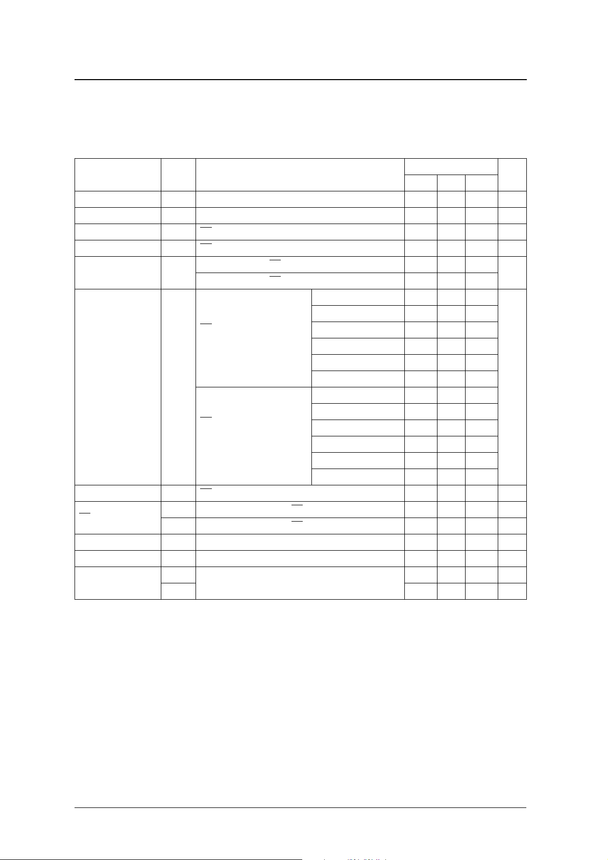
SPECIFICATIONS
Absolute Maximum Ratings
V
= 0V unless otherwise noted.
SS
Parameter Symbol Condition Rating Unit
Supply voltage range V
Input voltage range V
Output voltage range V
Operating temperature range T
Storage temperature range T
Output current I
Power dissipation P
DD
IN
OUT
opr
stg
OUT
−
−
SM5009 series
0.5 to +7.0 V
0.5 to V
+ 0.5 V
DD
−0.5 to V
Chip form −65 to +150
8-pin SOP −55 to +125
D
8-pin SOP 500 mW
+ 0.5 V
DD
−40 to +85 °C
25 mA
°C
Recommended Operating Conditions
V
= 0V unless otherwise noted.
SS
Parameter Symbol Version Condition
f ≤ 30MHz 4.5 – 5.5
f ≤ 16MHz 2.7 – 3.3
Chip form
8-pin SOP
f ≤ 30MHz, 4.5V ≤ VDD ≤ 5.5V − 40 – + 85
f ≤ 16MHz, 2.7V ≤ V
f ≤ 30MHz − 40 – + 85
30MHz < f ≤ 40MHz − 20 – + 80
Chip form
8-pin SOP
f ≤ 30MHz, 2.7V ≤ V
f ≤ 30MHz, 4.5V ≤ VDD ≤ 5.5V − 40 – + 85
Chip form
8-pin SOP
Supply voltage V
Input voltage V
Operating temperature T
AH×
AK× f ≤ 40MHz 4.5 – 5.5 V
AN× f ≤ 40MHz 2.7 – 5.5 V
CN× f ≤ 30MHz 2.7 – 5.5 V
DD
AL×
All version V
IN
AH×
AK×
AN×
OPR
CN×
AL×
Rating
min typ max
f ≤ 40MHz 2.7 – 5.5
f ≤ 30MHz 2.3 – 2.7
f ≤ 20MHz 2.25 – 2.75
f ≤ 40MHz 2.7 – 5.5
f ≤ 14.4MHz 2.4 – 2.7
SS
≤ 3.6V − 20 – + 80
DD
–VDDV
f ≤ 40MHz, 2.7V ≤ VDD < 4.5V − 20 – + 80
f ≤ 40MHz, 4.5V ≤ V
f ≤ 40MHz, 2.7V ≤ V
≤ 5.5V − 40 – + 85
DD
< 4.5V − 20 – + 80
DD
f ≤ 40MHz, 4.5V ≤ VDD ≤ 5.5V − 20 – + 80
f ≤ 30MHz, 4.5V ≤ V
< 4.5V − 10 – + 70
DD
f ≤ 40MHz, 2.7V ≤ V
f ≤ 30MHz, 2.3V ≤ V
≤ 5.5V − 40 – + 85
DD
≤ 5.5V − 40 – + 85
DD
≤ 2.7V − 20 – + 80
DD
f ≤ 20MHz, 2.25V ≤ VDD ≤ 2.75V − 20 – + 80
f ≤ 40MHz, 2.7V ≤ V
f ≤ 30MHz, 2.7V ≤ V
≤ 5.5V − 20 – + 80
DD
≤ 5.5V − 40 – + 85
DD
f ≤ 14.4MHz, 2.4V ≤ VDD ≤ 2.7V − 20 – + 80
Unit
V
V
°C
°C
°C
°C
°C
NIPPON PRECISION CIRCUITS INC.—5
Page 6
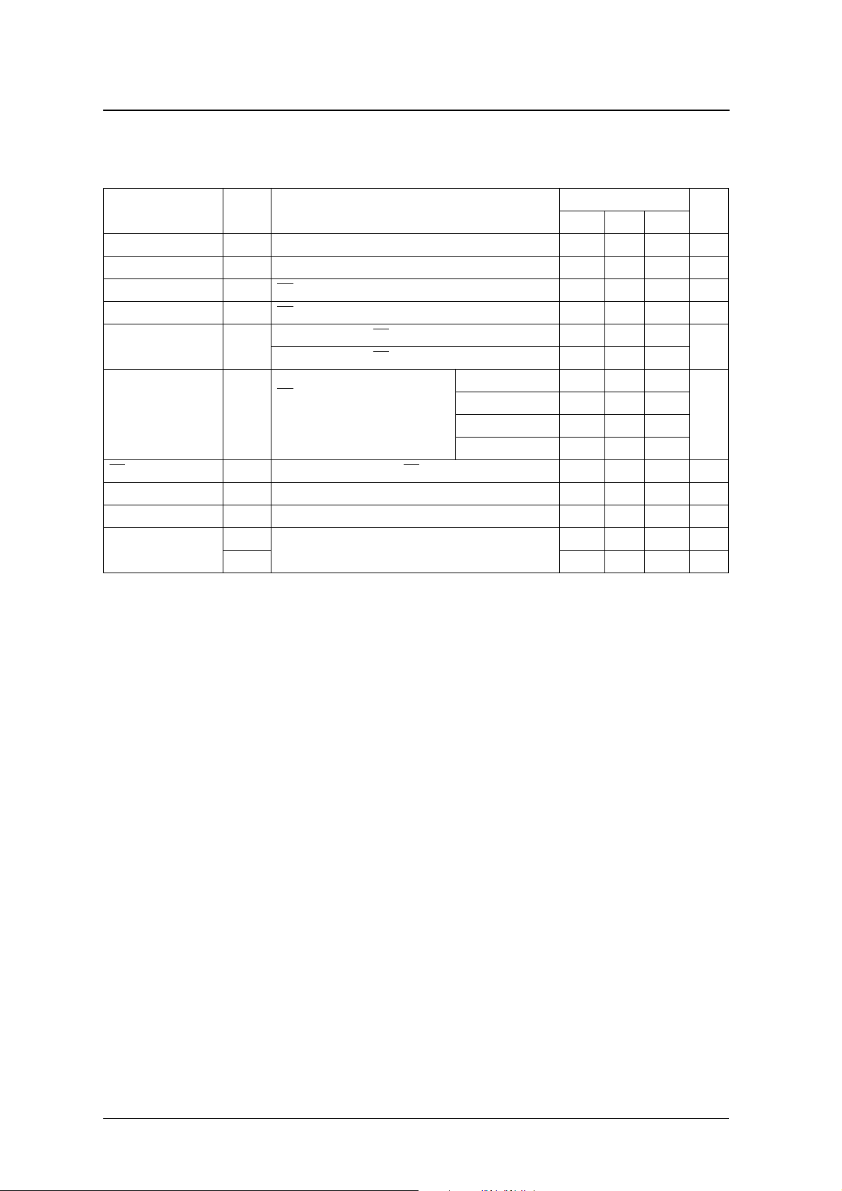
SM5009 series
Electrical Characteristics
5009AL× series
3V operation: VDD = 2.7 to 3.3V, VSS = 0V, Ta = −40 to 85°C unless otherwise noted.
Parameter Symbol Condition
Unit
min typ max
Rating
HIGH-level output voltage V
LOW-level output voltage V
HIGH-level input voltage V
LOW-level input voltage V
Output leakage current I
Q: Measurement cct 1, IOH = 8mA 2.2 – – V
OH
Q: Measurement cct 1, IOL = 8mA – – 0.4 V
OL
INH 0.7V
IH
INH – – 0.3V
IL
Q: Measurement cct 2, INH = LOW, VOH = V
Z
Q: Measurement cct 2, INH = LOW, VOL = V
DD
SS
––V
DD
––10
––10
DD
CF5009AL1 – 8 17
CF5009AL2 – 5 11
INH = open, Measurement cct 3,
CF5009AL3 – 4 9
load cct 2, CL = 15pF,
40MHz crystal oscillator
CF5009AL4 – 3 7
CF5009AL5 – 3 6
CF5009AL6 – 2 5
Current consumption I
DD
SM5009AL1S – 8 17
SM5009AL2S – 5 11
INH
= open, Measurement cct 3,
load cct 2, CL = 15pF,
40MHz crystal oscillator,
Ta = –20 to +80°C
SM5009AL3S – 4 9
SM5009AL4S – 3 7
SM5009AL5S – 3 6
SM5009AL6S – 2 5
Standby current I
INH pull-up resistance
INH = VSS, Measurement cct 3 – 2 5 µA
ST
R
Measurement cct 4, VDD = 3V, INH = V
UP1
R
Measurement cct 4, VDD = 3V, INH = 2.1V 40 – 200 kΩ
UP2
SS
0.6 – 12 MΩ
Negative resistance −RLVDD = 3V, Ta = 25°C, 40MHz – –200 – Ω
Feedback resistance R
Built-in capacitance
Measurement cct 5 0.4 – 1.1 MΩ
f
C
G
Design value. A monitor pattern on a wafer is tested.
C
D
5.58 6 6.42 pF
9.3 10 10.7 pF
V
µA
mA
NIPPON PRECISION CIRCUITS INC.—6
Page 7

SM5009 series
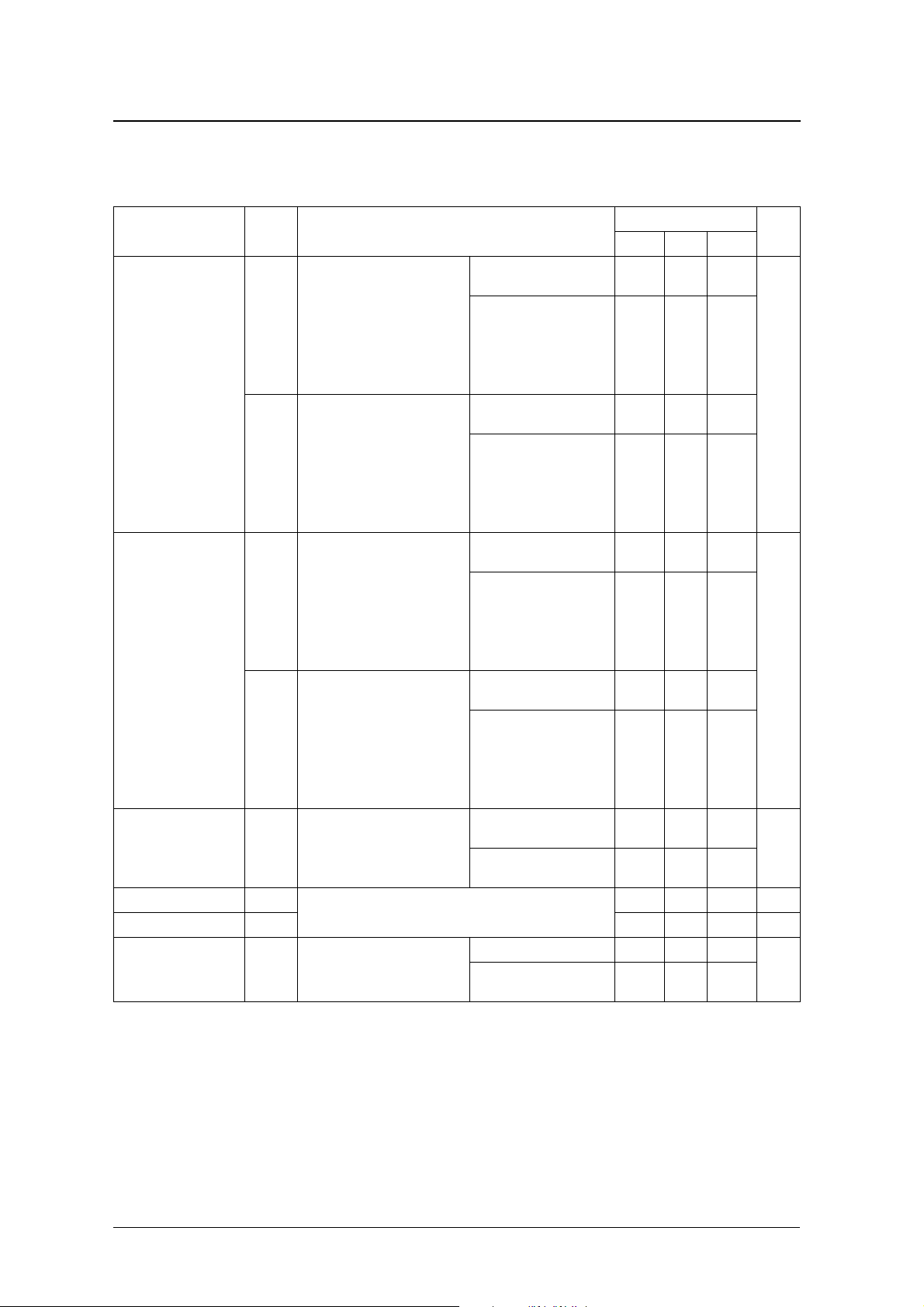
5V operation: VDD = 4.5 to 5.5V, VSS = 0V, Ta = −40 to 85°C unless otherwise noted.
Parameter Symbol Condition
Unit
min typ max
Rating
HIGH-level output voltage V
LOW-level output voltage V
HIGH-level input voltage V
LOW-level input voltage V
Output leakage current I
Q: Measurement cct 1, IOH = 16mA 4.0 – – V
OH
Q: Measurement cct 1, IOL = 16mA – – 0.4 V
OL
INH 0.7V
IH
INH – – 0.3V
IL
Q: Measurement cct 2, INH = LOW, VOH = V
Z
Q: Measurement cct 2, INH = LOW, VOL = V
DD
SS
––V
DD
––10
––10
DD
µA
CF5009AL1 – 12 26
CF5009AL2 – 8 17
INH = open, Measurement cct 3,
CF5009AL3 – 6 13
load cct 2, CL = 15pF,
40MHz crystal oscillator
CF5009AL4 – 5 11
CF5009AL5 – 5 10
CF5009AL6 – 4 9
Current consumption I
DD
SM5009AL1S – 12 26
mA
SM5009AL2S – 8 17
INH
= open, Measurement cct 3,
load cct 2, CL = 15pF,
40MHz crystal oscillator,
Ta = –20 to +80°C
SM5009AL3S – 6 13
SM5009AL4S – 5 11
SM5009AL5S – 5 10
SM5009AL6S – 4 9
Standby current I
INH pull-up resistance
INH = VSS, Measurement cct 3 – 6 15 µA
ST
R
Measurement cct 4, VDD = 5V, INH = V
UP1
R
Measurement cct 4, VDD = 5V, INH = 3.5V 40 – 200 kΩ
UP2
SS
0.3 – 6 MΩ
Negative resistance −RLVDD = 5V, Ta = 25°C, 40MHz – –400 – Ω
Feedback resistance RfMeasurement cct 5 0.4 – 1.1 MΩ
Built-in capacitance
C
G
Design value. A monitor pattern on a wafer is tested.
C
D
5.58 6 6.42 pF
9.3 10 10.7 pF
V
NIPPON PRECISION CIRCUITS INC.—7
Page 8

SM5009 series
5009AN×/CN× series
3V operation: VDD = 2.7 to 3.3V, VSS = 0V, Ta = −20 to 80°C unless otherwise noted.
Parameter Symbol Condition
SM5009AN1S, CF5009AN1
SM5009AN2S, CF5009AN2
min typ max
2.2 – –
Unit
SM5009AN3S, CF5009AN3
Rating
HIGH-level output voltage V
Q: Measurement cct 1, IOH = 8mA
OH
SM5009AN4S, CF5009AN4
SM5009AN5S, CF5009AN5
SM5009AN6S, CF5009AN6
2.1 – –
SM5009CN1S, CF5009CN1
SM5009CN2S, CF5009CN2
LOW-level output voltage V
HIGH-level input voltage V
LOW-level input voltage V
Output leakage current I
Q: Measurement cct 1, IOL = 8mA – – 0.4 V
OL
INH 2.0 – – V
IH
INH – – 0.3 V
IL
Q: Measurement cct 2, INH = LOW, VOH = V
Z
Q: Measurement cct 2, INH = LOW, VOL = V
DD
SS
––10
––10
SM5009AN1S, CF5009AN1 – 8 17
SM5009AN2S, CF5009AN2 – 5 11
Current consumption I
INH = open, Measurement cct 3,
load cct 2, CL = 15pF,
40MHz crystal oscillator
DD
SM5009AN3S, CF5009AN3 – 4 9
SM5009AN4S, CF5009AN4 – 3 7
SM5009AN5S, CF5009AN5 – 3 6
SM5009AN6S, CF5009AN6 – 2 5
INH
= open, Measurement cct 3,
SM5009CN1S, CF5009CN1 – 7 15
load cct 2, CL = 15pF,
INH
pull-up resistance R
30MHz crystal oscillator,
Ta = –10 to +70°C
Measurement cct 4, VDD = 3V, INH = V
UP
SM5009CN2S, CF5009CN2 – 4 9
SS
40 – 200 kΩ
Negative resistance −RLVDD = 3V, Ta = 25°C, 40MHz – –100 – Ω
Feedback resistance R
Built-in capacitance
Measurement cct 5 0.4 – 1.1 MΩ
f
C
G
Design value. A monitor pattern on a wafer is tested.
C
D
5.58 6 6.42 pF
9.3 10 10.7 pF
V
µA
mA
NIPPON PRECISION CIRCUITS INC.—8
Page 9

SM5009 series
5V operation: VDD = 4.5 to 5.5V, VSS = 0V, Ta = −40 to 85°C unless otherwise noted.
Parameter Symbol Condition
HIGH-level output voltage V
LOW-level output voltage V
HIGH-level input voltage V
LOW-level input voltage V
Q: Measurement cct 1, IOH = 16mA
OH
Q: Measurement cct 1, IOL = 16mA – – 0.4 V
OL
INH 2.0 – – V
IH
INH – – 0.8 V
IL
Q: Measurement cct 2, INH = LOW, VOH = V
Output leakage current I
Z
Q: Measurement cct 2, INH = LOW, VOL = V
INH = open, Measurement cct 3,
load cct 2, CL = 15pF,
40MHz crystal oscillator
Current consumption I
DD
= open, Measurement cct 3,
INH
load cct 2, CL = 15pF,
40MHz crystal oscillator,
Ta = –20 to +80°C
INH
= open, Measurement cct 3,
INH pull-up resistance R
Negative resistance −R
Feedback resistance R
Built-in capacitance
load cct 2, C
30MHz crystal oscillator
Measurement cct 4, VDD = 5V, INH = V
UP
LVDD
Measurement cct 5 0.4 – 1.1 MΩ
f
C
G
Design value. A monitor pattern on a wafer is tested.
C
D
= 15pF,
L
= 5V, Ta = 25°C, 40MHz – –210 – Ω
Rating
min typ max
SM5009AN1S, CF5009AN1
SM5009AN2S, CF5009AN2
4.0 – –
SM5009AN3S, CF5009AN3
SM5009AN4S, CF5009AN4
SM5009AN5S, CF5009AN5
SM5009AN6S, CF5009AN6
3.9 – –
SM5009CN1S, CF5009CN1
SM5009CN2S, CF5009CN2
DD
SS
––10
––10
CF5009AN1 – 12 26
CF5009AN2 – 8 17
CF5009AN3 – 6 13
CF5009AN4 – 5 11
CF5009AN5 – 5 10
CF5009AN6 – 4 9
SM5009AN1S – 12 26
SM5009AN2S – 8 17
SM5009AN3S – 6 13
SM5009AN4S – 5 11
SM5009AN5S – 5 10
SM5009AN6S – 4 9
SM5009CN1S, CF5009CN1 – 10 22
SM5009CN2S, CF5009CN2 – 7 15
SS
40 – 200 kΩ
5.58 6 6.42 pF
9.3 10 10.7 pF
Unit
V
µA
mA
NIPPON PRECISION CIRCUITS INC.—9
Page 10
SM5009 series
5009AK× series
VDD = 4.5 to 5.5V, VSS = 0V, Ta = −40 to 85°C unless otherwise noted.
Parameter Symbol Condition
HIGH-level output voltage V
LOW-level output voltage V
HIGH-level input voltage V
LOW-level input voltage V
Q: Measurement cct 1, IOH = 16mA 4.0 – – V
OH
Q: Measurement cct 1, IOL = 16mA – – 0.4 V
OL
INH 2.0 – – V
IH
INH – – 0.8 V
IL
Q: Measurement cct 2, INH = LOW, VOH = V
Output leakage current I
Z
Q: Measurement cct 2, INH = LOW, VOL = V
min typ max
DD
SS
––10
––10
Unit
µA
SM5009AK1S – 12 26
Rating
Current consumption I
INH = open, Measurement cct 3,
load cct 1, CL = 15pF,
DD
40MHz crystal oscillator,
Ta = –20 to +80°C
CF5009AK1 – 12 26
mA
SM5009AK2S – 8 17
CF5009AK2 – 8 17
pull-up resistance R
INH
Measurement cct 4, VDD = 5V, INH = V
UP
SS
40 – 200 kΩ
Negative resistance −RLVDD = 5V, Ta = 25°C, 40MHz – –210 – Ω
Feedback resistance RfMeasurement cct 5 0.4 – 1.1 MΩ
Built-in capacitance
C
G
Design value. A monitor pattern on a wafer is tested.
C
D
5.58 6 6.42 pF
9.3 10 10.7 pF
NIPPON PRECISION CIRCUITS INC.—10
Page 11

SM5009 series
5009AH× series
3V operation: VDD = 2.7 to 3.3V, VSS = 0V, Ta = −20 to 80°C unless otherwise noted.
Parameter Symbol Condition
HIGH-level output voltage V
LOW-level output voltage V
HIGH-level input voltage V
LOW-level input voltage V
Output leakage current I
Q: Measurement cct 1, IOH = 2mA 2.2 – – V
OH
Q: Measurement cct 1, IOL = 2mA – – 0.4 V
OL
INH 2.0 – – V
IH
INH – – 0.3 V
IL
Q: Measurement cct 2, INH = LOW, VOH = V
Z
Q: Measurement cct 2, INH = LOW, VOL = V
INH = open, Measurement cct 3,
Current consumption I
load cct 2, CL = 15pF,
DD
16MHz crystal oscillator
DD
SS
SM5009AH1S
CF5009AH1
SM5009AH2S
CF5009AH2
SM5009AH3S
CF5009AH3
SM5009AH4S
Rating
min typ max
––10
––10
– 4.5 10
–37
– 1.5 3.5
Unit
µA
mA
CF5009AH4
INH
pull-up resistance R
Measurement cct 4, VDD = 3V, INH = V
UP
SS
40 – 200 kΩ
Negative resistance −RLVDD = 3V, Ta = 25°C, 16MHz – –450 – Ω
Feedback resistance RfMeasurement cct 5 0.4 – 1.1 MΩ
Built-in capacitance
C
G
Design value. A monitor pattern on a wafer is tested.
C
D
5.58 6 6.42 pF
9.3 10 10.7 pF
5V operation: VDD = 4.5 to 5.5V, VSS = 0V, Ta = −40 to 85°C unless otherwise noted.
Parameter Symbol Condition
HIGH-level output voltage V
LOW-level output voltage V
HIGH-level input voltage V
LOW-level input voltage V
Output leakage current I
Q: Measurement cct 1, IOH = 4mA 4.0 – – V
OH
Q: Measurement cct 1, IOL = 4mA – – 0.4 V
OL
INH 2.0 – – V
IH
INH – – 0.8 V
IL
Q: Measurement cct 2, INH = LOW, VOH = V
Z
Q: Measurement cct 2, INH = LOW, VOL = V
DD
SS
SM5009AH1S
CF5009AH1
SM5009AH2S
CF5009AH2
SM5009AH3S
Current consumption I
INH = open, Measurement cct 3,
load cct 2, C
DD
30MHz crystal oscillator
= 15pF,
L
CF5009AH3
SM5009AH4S
CF5009AH4
INH
pull-up resistance R
Measurement cct 4, VDD = 5V, INH = V
UP
SS
Negative resistance −RLVDD = 5V, Ta = 25°C, 30MHz – –340 – Ω
Feedback resistance RfMeasurement cct 5 0.4 – 1.1 MΩ
C
Built-in capacitance
G
Design value. A monitor pattern on a wafer is tested.
C
D
Rating
min typ max
––10
––10
–920
–613
–49
40 – 200 kΩ
5.58 6 6.42 pF
9.3 10 10.7 pF
Unit
µA
mA
NIPPON PRECISION CIRCUITS INC.—11
Page 12

SM5009 series
Switching Characteristics
5009AL× series
3V operation: VDD = 2.7 to 3.3V, VSS = 0V, Ta = −40 to 85°C unless otherwise noted.
Parameter Symbol Condition
Unit
min typ max
Rating
Output rise time
Output fall time
Output duty cycle
1
Output disable delay time
Output enable delay time
Measurement cct 3, load cct 2, 0.1VDD to 0.9V
t
r1
Measurement cct 3, load cct 2, 0.1VDD to 0.9V
VDD = 2.3 to 2.7V, Ta = –20 to +80°C, CL = 15pF
Measurement cct 3, load cct 2, 0.1VDD to 0.9V
t
r2
Measurement cct 3, load cct 2, 0.1VDD to 0.9V
VDD = 2.4 to 2.7V, Ta = –20 to +80°C, CL = 30pF
Measurement cct 3, load cct 2, 0.1VDD to 0.9V
VDD = 3.0 to 3.6V, f ≤ 30MHz, CL = 50pF
t
r3
Measurement cct 3, load cct 2, 0.2VDD to 0.8V
VDD = 3.0 to 3.6V, f ≤ 40MHz, CL = 50pF
Measurement cct 3, load cct 2, 0.9VDD to 0.1V
t
f1
Measurement cct 3, load cct 2, 0.9VDD to 0.1V
VDD = 2.3 to 2.7V, Ta = –20 to +80°C, CL = 15pF
Measurement cct 3, load cct 2, 0.9VDD to 0.1V
t
f2
Measurement cct 3, load cct 2, 0.9VDD to 0.1V
VDD = 2.4 to 2.7V, Ta = –20 to +80°C, CL = 30pF
Measurement cct 3, load cct 2, 0.9VDD to 0.1V
VDD = 3.0 to 3.6V, f ≤ 30MHz, CL = 50pF
t
f3
Duty1
Measurement cct 3, load cct 2, 0.8V
VDD = 3.0 to 3.6V, f ≤ 40MHz, CL = 50pF
Measurement cct 3, load cct 2, V
CL = 30pF
Measurement cct 3, load cct 2, V
CL = 30pF
to 0.2V
DD
= 3V, f ≤ 40MHz, Ta = 25°C,
DD
= 2.4V, f ≤ 14.4MHz, Ta = 25°C,
DD
CF5009AL× only, Measurement cct 3, load cct 2, V
f ≤ 30MHz, Ta = 25°C, C
= 15pF
L
CF5009AL× only, Measurement cct 3, load cct 2, V
f ≤ 30MHz, Ta = 25°C, CL = 50pF
Duty2
CF5009AL× only, Measurement cct 3, load cct 2, VDD = 3.3V,
f ≤ 40MHz, Ta = 25°C, CL = 50pF
2
t
PLZ
2
Measurement cct 6, load cct 2, VDD = 3V, Ta = 25°C, CL ≤ 15pF
t
PZL
, CL = 15pF – 3.5 9
DD
,
DD
, CL = 30pF – 5 12
DD
,
DD
,
DD
,
DD
, CL = 15pF – 3.5 9
DD
,
DD
, CL = 30pF – 5 12
DD
,
DD
,
DD
,
DD
–413
– 5.5 16
–512
– 3.5 12
–413
– 5.5 16
–512
– 3.5 12
45–55
40–60
= 2.5V,
DD
DD
= 3.3V,
40–60
45–55
40–60
– – 100 ns
– – 100 ns
ns
ns
%
CF5009AL× 40 – –
Measurement cct 3
SM5009AL×S30––
Measurement cct 3, Ta = –20 to +80°C SM5009AL×S40––
= 2.4 to 2.7V,
Maximum operating
frequency
f
max
Measurement cct 3, Ta = –20 to +80°C
V
DD
SM5009AL×S
VDD = 2.3 to 2.7V,
CF5009AL×
VDD = 2.25 to 2.75V,
CF5009AL×
14.4 – –
30 – –
20 – –
MHz
1. The duty cycle characteristic is checked the sample chips of each production lot.
2. Oscillator stop function is built-in. When INH goes LOW, normal output stops. When INH goes HIGH, normal output is not resumed until after the
oscillator start-up time has elapsed.
NIPPON PRECISION CIRCUITS INC.—12
Page 13

SM5009 series
5V operation: VDD = 4.5 to 5.5V, VSS = 0V, Ta = −40 to 85°C unless otherwise noted.
Parameter Symbol Condition
Unit
min typ max
Rating
Output rise time
Output fall time
Output duty cycle
Output disable delay time
1
2
Output enable delay time2t
t
r1
Measurement cct 3, load cct 2,
r2
0.1VDD to 0.9V
t
r3
t
f1
Measurement cct 3, load cct 2,
f2
0.9VDD to 0.1V
t
f3
DD
DD
Duty Measurement cct 3, load cct 2, VDD = 5V, Ta = 25°C, CL = 50pF 45 – 55 %
t
PLZ
Measurement cct 6, load cct 2, VDD = 5V, Ta = 25°C, CL ≤ 15pF
PZL
CL = 15pF – 2 4
CL = 30pF – 3.5 7
CL = 50pF – 4 8
CL = 15pF – 2 4
CL = 30pF – 3.5 7
CL = 50pF – 4 8
– – 100 ns
– – 100 ns
nst
nst
CF5009AL× 40 – –
Maximum operating
frequency
f
max
Measurement cct 3
MHzSM5009AL×S30––
Measurement cct 3, Ta = –20 to +80°C SM5009AL×S40––
1. The duty cycle characteristic is checked the sample chips of each production lot.
2. Oscillator stop function is built-in. When INH goes LOW, normal output stops. When INH goes HIGH, normal output is not resumed until after the
oscillator start-up time has elapsed.
NIPPON PRECISION CIRCUITS INC.—13
Page 14
SM5009 series
5009AN×/CN× series
3V operation: VDD = 2.7 to 3.3V, VSS = 0V, Ta = −20 to 80°C unless otherwise noted.
Parameter Symbol Condition
SM5009AN1S, CF5009AN1
SM5009AN2S, CF5009AN2
Measurement cct 3, load cct 2,
t
r1
0.1VDD to 0.9V
DD ,CL
= 15pF
SM5009AN3S, CF5009AN3
SM5009AN4S, CF5009AN4
SM5009AN5S, CF5009AN5
SM5009AN6S, CF5009AN6
SM5009CN1S, CF5009CN1
Output rise time
SM5009CN2S, CF5009CN2
SM5009AN1S, CF5009AN1
SM5009AN2S, CF5009AN2
Measurement cct 3, load cct 2,
t
r2
0.1VDD to 0.9V
DD ,CL
= 30pF
SM5009AN3S, CF5009AN3
SM5009AN4S, CF5009AN4
SM5009AN5S, CF5009AN5
SM5009AN6S, CF5009AN6
SM5009CN1S, CF5009CN1
SM5009CN2S, CF5009CN2
SM5009AN1S, CF5009AN1
SM5009AN2S, CF5009AN2
Measurement cct 3, load cct 2,
t
f1
0.9VDD to 0.1V
DD ,CL
= 15pF
SM5009AN3S, CF5009AN3
SM5009AN4S, CF5009AN4
SM5009AN5S, CF5009AN5
SM5009AN6S, CF5009AN6
SM5009CN1S, CF5009CN1
SM5009CN2S, CF5009CN2
Output fall time
SM5009AN1S, CF5009AN1
SM5009AN2S, CF5009AN2
Measurement cct 3, load cct 2,
t
f2
0.9VDD to 0.1V
DD ,CL
= 30pF
SM5009AN3S, CF5009AN3
SM5009AN4S, CF5009AN4
SM5009AN5S, CF5009AN5
SM5009AN6S, CF5009AN6
SM5009CN1S, CF5009CN1
SM5009CN2S, CF5009CN2
C
Output duty cycle
1
Measurement cct 3, load cct 2,
Duty
= 3V, Ta = 25°C
V
DD
SM5009AN×S, CF5009AN×
C
SM5009CN×S, CF5009CN×
Output disable delay time t
Output enable delay time t
PLZ
Measurement cct 6, load cct 2, VDD = 3V, Ta = 25°C, CL ≤ 15pF
PZL
SM5009AN×S, CF5009AN× 40 – –
Maximum operating
frequency
f
max
Measurement cct 3
Ta = –10 to +70°C,
SM5009CN×S, CF5009CN×
1. The duty cycle characteristic is checked the sample chips of each production lot.
= 30 pF,
L
= 15 pF,
L
Rating
min typ max
– 3.5 9
–513
–512
–716
– 3.5 9
–513
–512
–716
45–55
40–60
– – 100 ns
– – 100 ns
30 – –
Unit
ns
ns
%
MHz
NIPPON PRECISION CIRCUITS INC.—14
Page 15

SM5009 series
5V operation: VDD = 4.5 to 5.5V, VSS = 0V, Ta = −40 to 85°C unless otherwise noted.
Parameter Symbol Condition
Output rise time
Output fall time
Output duty cycle
1
Output disable delay time t
Output enable delay time t
Maximum operating
frequency
t
r1
Measurement cct 3, load cct 2,
r2
0.1VDD to 0.9V
t
r3
t
f1
Measurement cct 3, load cct 2,
f2
0.9VDD to 0.1V
t
f3
DD
DD
Duty Measurement cct 3, load cct 2, VDD = 5V, Ta = 25°C, CL = 50pF 45 – 55 %
PLZ
Measurement cct 6, load cct 2, VDD = 5V, Ta = 25°C, CL ≤ 15pF
PZL
f
Measurement cct 3
max
CL = 15pF – 2 4
CL = 30pF – 3.5 7
CL = 50pF – 4 8
CL = 15pF – 2 4
CL = 30pF – 3.5 7
CL = 50pF – 4 8
SM5009AN×S, CF5009AN× 40 – –
SM5009CN×S, CF5009CN× 30 – –
1. The duty cycle characteristic is checked the sample chips of each production lot.
5009AK× series
VDD = 4.5 to 5.5V, VSS = 0V, Ta = −40 to 85°C unless otherwise noted.
Parameter Symbol Condition
Output rise time t
Output fall time t
Output duty cycle
1
Output disable delay time t
Output enable delay time t
Maximum operating
frequency
Measurement cct 3, load cct 1, 0.4V to 2.4V, CL = 15pF – 2 6 ns
r
Measurement cct 3, load cct 1, 2.4V to 0.4V, CL = 15pF – 2 6 ns
f
Duty Measurement cct 3, load cct 1, VDD = 5V, Ta = 25°C, CL = 15pF 45 – 55 %
PLZ
Measurement cct 6, load cct 1, VDD = 5V, Ta = 25°C, CL ≤ 15pF
PZL
f
max
Measurement cct 3
Ta = –20 to +80°C40––
Ta = –40 to +85°C30––
Rating
Unit
min typ max
nst
nst
– – 100 ns
– – 100 ns
MHz
Rating
Unit
min typ max
– – 100 ns
– – 100 ns
MHz
1. The duty cycle characteristic is checked the sample chips of each production lot.
NIPPON PRECISION CIRCUITS INC.—15
Page 16

SM5009 series
5009AH× series
3V operation: VDD = 2.7 to 3.3V, VSS = 0V, Ta = −20 to 80°C unless otherwise noted.
Parameter Symbol Condition
Output rise time t
Output fall time t
Output duty cycle
1
Output disable delay time t
Output enable delay time t
Maximum operating
frequency
Measurement cct 3, load cct 2, 0.1VDD to 0.9V
r1
Measurement cct 3, load cct 2, 0.9VDD to 0.1V
f1
Duty Measurement cct 3, load cct 2, VDD = 3V, Ta = 25°C, CL = 15pF 45 – 55 %
PLZ
Measurement cct 6, load cct 2, VDD = 3V, Ta = 25°C, CL ≤ 15pF
PZL
Measurement cct 3 16 – – MHz
f
max
, CL = 15pF – 6 18 ns
DD
, CL = 15pF – 6 18 ns
DD
min typ max
1. The duty cycle characteristic is checked the sample chips of each production lot.
5V operation: VDD = 4.5 to 5.5V, VSS = 0V, Ta = −40 to 85°C unless otherwise noted.
Parameter Symbol Condition
Output rise time t
Output fall time t
Output duty cycle
1
Output disable delay time t
Output enable delay time t
Maximum operating
frequency
Measurement cct 3, load cct 2, 0.1VDD to 0.9V
r1
Measurement cct 3, load cct 2, 0.9VDD to 0.1V
f1
Duty Measurement cct 3, load cct 2, VDD = 5V, Ta = 25°C, CL = 15pF 45 – 55 %
PLZ
Measurement cct 6, load cct 2, VDD = 5V, Ta = 25°C, CL ≤ 15pF
PZL
f
Measurement cct 3 30 – – MHz
max
1. The duty cycle characteristic is checked the sample chips of each production lot.
, CL = 15pF – 4 12 ns
DD
, CL = 15pF – 4 12 ns
DD
min typ max
Rating
Unit
– – 100 ns
– – 100 ns
Rating
Unit
– – 100 ns
– – 100 ns
NIPPON PRECISION CIRCUITS INC.—16
Page 17

MEASUREMENT CIRCUITS
SM5009 series
Measurement cct 1
Signal
Generator
XT input waveform
(10MHz)
Q output
Q output
R1
• 5009AK×, AL×, AN1, AN2
R1: 50Ω
R2: 250Ω(VDD = 4.5V), 275Ω(VDD = 2.7V)
R3: 256Ω(VDD = 4.5V), 288Ω(VDD = 2.7V)
• 5009AN3 to AN6, CN×
R1: 50Ω
R2: 245Ω(V
R3: 256Ω(VDD = 4.5V), 288Ω(VDD = 2.7V)
= 4.5V), 262Ω(VDD = 2.7V)
DD
• 5009AH×
R1: 50Ω
R2: 1000Ω(VDD = 4.5V), 1100Ω(VDD = 2.7V)
R3: 1025Ω(VDD = 4.5V), 1150Ω(VDD = 2.7V)
XT Q
Measurement cct 2
VDD
VSS
When
measuring
When
measuring
V
0V
V
V
0V
V
V
0V
Measurement cct 4
V
OL
R3
R2
V
OH
DD
DD
OH
DD
OL
VSS
3.0V or 5.0V
VDD
V
VIH
VIL
INH
A
IPR
RUP
RUP1
RUP2 =
VDD
=
IPR
DD VIH
V
I
PR
(VIL = 0V)
VIH : 2.1V(V DD = 3.0V)
V
IH : 3.5V(V DD = 5.0V)
Measurement cct 5
VDD
XT
XT
VSS
A
Rf =
DD
V
I
Rf
VDD
Q
VSS
Measurement cct 3
XT
XT
INH
A
VDD
V
VSS
I
Rf
I
Z
I
Z
A
Measurement cct 6
V
OH
V
OL
VDD
IDD
IST
Signal
Generator
R1
QX'tal
R1: 50Ω
XT Q
VSS
INH
NIPPON PRECISION CIRCUITS INC.—17
Page 18

SM5009 series
Load cct 1 Load cct 2
R
Q output
C
(Including probe
CL = 15pF: DUTY, IDD, tr, t
R = 400Ω
capacitance)
f
L
Switching Time Measurement Waveform
Output duty level (CMOS)
Q output
0.9VDD
0.1VDD
TW
tr tf
Output duty level (TTL)
Q output
CL = 15pF: DUTY, IDD, tr1, t
CL = 30pF: tr2, t
CL = 50pF: tr3, t
f2
f3
0.9VDD
0.1VDD
C
L
(Including probe
f1
DUTY measurement
voltage (0.5V
DD)
capacitance)
Q output
Output duty cycle (CMOS)
Q output
Output duty cycle (TTL)
Q output
2.4V
0.4V
TW
tr tf
TW
T
TW
T
2.4V
0.4V
DUTY measurement
voltage (1.4V
DUTY measurement
voltage
DUTY= T
DUTY measurement
voltage
DUTY= T
)
(0.5VDD)
W/ T 100 (%)
(1.4V)
W/ T 100 (%)
NIPPON PRECISION CIRCUITS INC.—18
Page 19

Output Enable/Disable Delay
SM5009 series
INH
VIL
tPLZ
VIH
tPZL
Q output
INH input waveform tr = tf 10ns
Note (AL× series only): when the device is in standby, the oscillator stops. When standby is released, the oscil-
lator starts and stable oscillator output occurs after a short delay.
NIPPON PRECISION CIRCUITS INC.—19
Page 20

SM5009 series
Please pay your attention to the following points at time of using the products shown in this document.
The products shown in this document (hereinafter “Products”) are not intended to be used for the apparatus that exerts harmful influence on
human lives due to the defects, failure or malfunction of the Products. Customers are requested to obtain prior written agreement for such
use from NIPPON PRECISION CIRCUITS INC. (hereinafter “NPC”). Customers shall be solely responsible for, and indemnify and hold NPC
free and harmless from, any and all claims, damages, losses, expenses or lawsuits, due to such use without such agreement. NPC reserves
the right to change the specifications of the Products in order to improve the characteristic or reliability thereof. NPC makes no claim or
warranty that the contents described in this document dose not infringe any intellectual property right or other similar right owned by third
parties. Therefore, NPC shall not be responsible for such problems, even if the use is in accordance with the descriptions provided in this
document. Any descriptions including applications, circuits, and the parameters of the Products in this document are for reference to use the
Products, and shall not be guaranteed free from defect, inapplicability to the design for the mass-production products without further testing
or modification. Customers are requested not to export or re-export, directly or indirectly, the Products to any country or any entity not in
compliance with or in violation of the national export administration laws, treaties, orders and regulations. Customers are requested
appropriately take steps to obtain required permissions or approvals from appropriate government agencies.
NIPPON PRECISION CIRCUITS INC.
4-3, Fukuzumi 2-chome, Koto-ku,
Tokyo 135-8430, Japan
Telephone: +81-3-3642-6661
Facsimile: +81-3-3642-6698
http://www.npc.co.jp/
Email: sales
@npc.co.jp
NC9801GE 2003.07
NIPPON PRECISION CIRCUITS INC.—20
 Loading...