


查询CF5002LA供应商查询CF5002LA供应商
SM5002L series
NIPPON PRECISION CIRCUITS INC.
Crystal Oscillator Module ICs
OVERVIEW
The SM5002L series crystal oscillator module ICs fabricated in NPC’s Molybdenum-gate CMOS. They
comprise low-voltage low-current consumption oscillator circuits and output buffers. They incorporate built-in
oscillation capacitance with superior frequency response to realize stable 3rd overtone oscillation without any
external components.
FEATURES
■
Oscillation frequency up to 100 MHz
■
Third harmonic
■
Capacitors C
■
Standby function (oscillator stops)
■
3 µA (typ) low standby current
■
Inverter amplifier feedback resistance built-in
■
INH pin pull-up resistance built-in
and C
G
built-in
D
• INH= L : 2M Ω typ
■
CMOS input level
■
8 mA (V
■
CMOS output duty level
■
Output three-state function
■
2.7 to 3.6 V supply voltage
■
Oscillator frequency output
■
8-pin SOP (SM5002L × S)
■
Chip form (CF5002L × )
= 3.0 V) output drive capability
DD
• INH= H : 90k Ω typ
SERIES CONFIGURATION
Version
CF5002LA
SM5002LAS
CF5002LB
SM5002LBS
CF5002LC
SM5002LCS
CF5002LD
SM5002LDS
CF5002LE
SM5002LES
CF5002LF
SM5002LFS
Recommended
operating
frequency range
(MHz)
30 to 40 1.0 8 15 5.6 22 CMOS 8 Yes
40 to 50 1.5 8 15 4.7 22 CMOS 8 Yes
50 to 70 1.5 8 10 3.9 22 CMOS 8 Yes
70 to 90 2.0 8 10 3.9 22 CMOS 8 Yes
85 to 100 2.0 8 10 2.7 22 CMOS 8 Yes
25 to 30 1.0 10 15 8.5 22 CMOS 8 Yes
g
m
(relative
value)
ORDERING INFORMATION
Device Package
SM5002L × S 8-pin SOP
CF5002L ×
Chip form
Built-in capacitance
C
(pF) C
G
D
(pF)
R
(k Ω )
f1
C
(pF)
f
Output
duty level
Output
current
(mA)
Standby
function
NIPPON PRECISION CIRCUITS—1
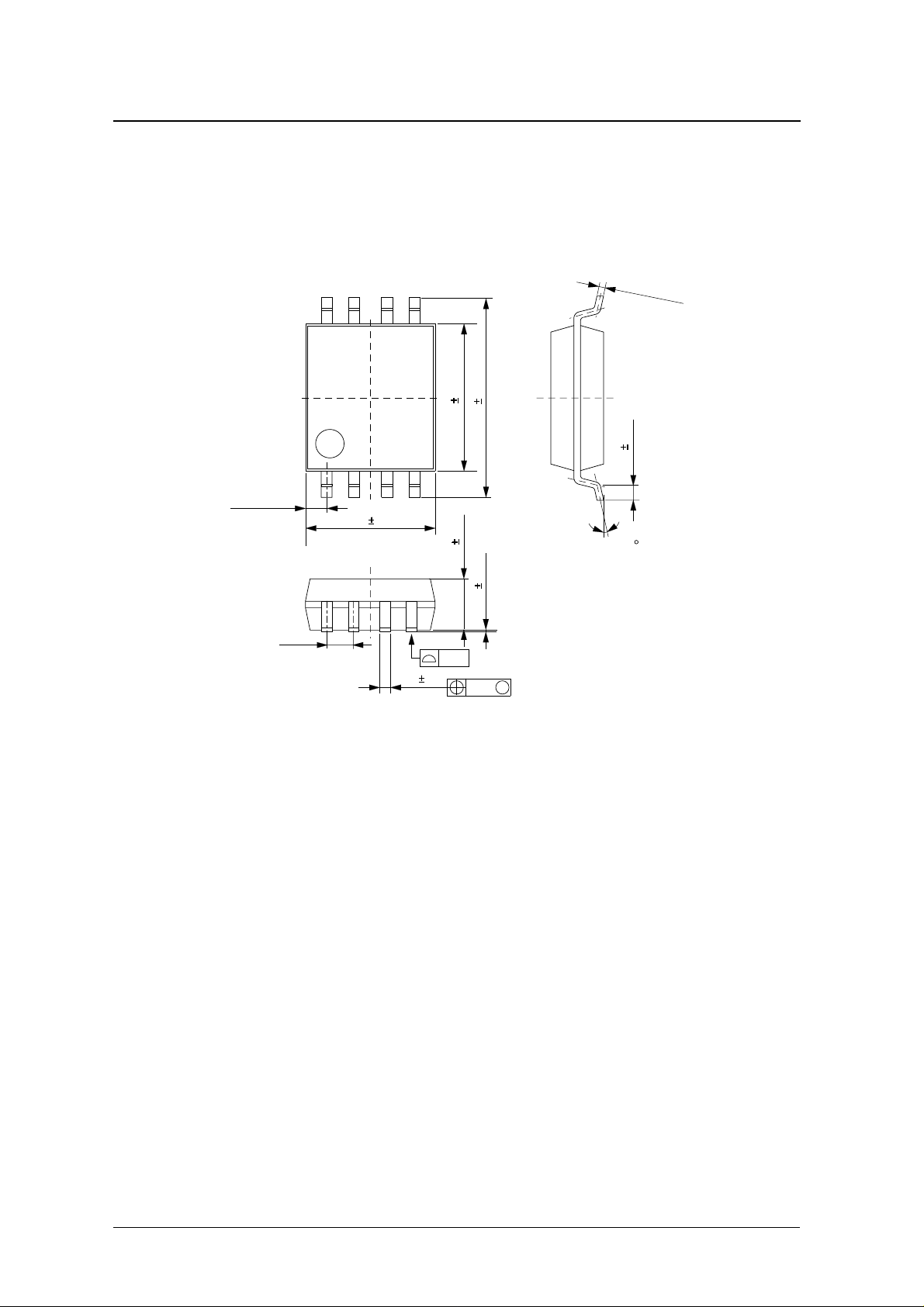
•
PACKAGE DIMENSIONS
(UNIT : mm)
8-pin SOP
SM5002L series
6.2 0.3
4.4 0.2
0.15
+ 0.1
− 0.05
0.695TYP
1.27
5.2 0.3
0.4 0.1
1.5 0.1
0.10
0.05 0.05
M
0.12
0.4 0.2
0 to 10
NIPPON PRECISION CIRCUITS—2
SM5002L series
PAD LAYOUT
(Unit : µ m)
Y
(0,0)
Chip size: 0.92
Chip thickness: 400 ± 30 µm
Chip base: V
INH
QVDD
HA5002L
XT
XT VSS
X
× 1.31 mm
level
DD
(920,1310)
PINOUT
(T op V iew)
INH
XT
XT
VSS
1
2
3
4
8
5002L
7
6
5
PIN DESCRIPTION and PAD DIMENSIONS
Number Name I/O Description
1 INH I
2 XT I Amplifier input.
3XTO Amplifier output. 575 188
4 VSS – Ground 766 188
5 Q O Output. Output frequency. High impedance at standby operation 765 1159
6 NC – No connection – –
7 NC – No connection – –
8 VDD – Supply voltage 162 1159
Output state control input. Oscillator stopped when LOW. Power-saving pull-up
resistor built in
Crystal oscillator connection pins.
Crystal oscillator connected between XT and XT
Pad dimensions [µm]
XY
195 188
385 188
VDD
NC
NC
Q
BLOCK DIAGRAM
XT
XT
INH
VSSVDD
CG CD
Rf 1
Cf
Rf 2
RUP1/RUP2
Q
NIPPON PRECISION CIRCUITS—3

SPECIFICATIONS
Absolute Maximum Ratings
V
= 0 V unless otherwise noted.
SS
Parameter Symbol Condition Rating Unit
Supply voltage range V
Input voltage range V
Output voltage range V
Operating temperature range T
Storage temperature range
Output current I
Power dissipation P
Soldering temperature T
Soldering time t
T
T
DD
OUT
opr
stg1
stg2
OUT
sld
sld
−
−
−
−
−
−
°
SM5002L series
0.5 to 7.0 V
0.5 to V
IN
Chip form
8-pin SOP
D
Ta ≤ 85 ° C, 8-pin SOP 200 mW
8-pin SOP 255
8-pin SOP 10 s
+ 0.5 V
DD
0.5 to V
+ 0.5 V
DD
40 to 85
− 65 to 150
− 40 to 125
25 mA
° C
° C
° C
Recommended Operating Conditions
CF5002L × series (Chip form)
V
= 0 V unless otherwise noted.
SS
Parameter Symbol Conditions
C
≤ 15pF, f ≤ 70 MHz 2.7 – 3.6 V
L
Supply voltage V
Input voltage V
Operating temperature T
SM5002L × S series (8-pin SOP)
V
= 0 V unless otherwise noted.
SS
Parameter Symbol Conditions
Supply voltage V
Input voltage V
Operating temperature T
DD
IN
OPR
DD
IN
OPR
C
≤ 15pF, 70 < f ≤ 100 MHz 3.0 – 3.6 V
L
C
≤ 30pF, f ≤ 70 MHz 3.0 – 3.6 V
L
C
≤ 15pF, f ≤ 50 MHz 2.7 – 3.6 V
L
C
≤ 15pF, 50 < f ≤ 70 MHz 3.0 – 3.6 V
L
C
≤ 30pF, f ≤ 50 MHz 3.0 – 3.6 V
L
Limits
min typ max
V
SS
–V
DD
20 – 80
Limits
min typ max
V
SS
–V
DD
20 – 80
Units
V
° C
Units
V
C
NIPPON PRECISION CIRCUITS—4

Electrical Characteristics
V
= 2.7 to 3.6 V, V
DD
= 0 V, T
SS
SM5002L series
= − 20 to 80 ° C, unless otherwise noted.
a
Parameter Symbol Conditions
Units
min typ max
Limits
HIGH-level output voltage V
LOW-level output voltage V
Output leakage current I
HIGH-level input voltage V
LOW-level input voltage V
Q: Measurement cct 1, V
OH
Q: Measurement cct 2, V
OL
Q: Measurement cct 2,
Z
INH = LOW , V
INH pin 0.7V
IH
INH pin – – 0.3V
IL
DD
= 3.6V
= 2.7 V, I
DD
= 2.7 V, I
DD
V
OH
V
OL
= 8 mA 2.2 2.4 – V
OH
= 8 mA – 0.3 0.4 V
OL
= V
= V
DD
SS
– – 10 µA
– – 10 µA
DD
––V
DD
SM5002LAS, SM5002LFS
–1018mA
–1525mA
–2035mA
Current consumption I
INH = open,
Measurement cct 3,
DD
load cct 1,
V
= 3.0 to 3.6 V
DD
CF5002LA, CF5002LF
= 30 pF, f = 30 MHz
C
L
SM5002LBS, CF5002LB
C
= 30 pF, f = 50 MHz
L
SM5002LCS, CF5002LC
C
= 30 pF, f = 70 MHz
L
SM5002LDS, SM5002LES
Standby current I
INH pull-up resistance
CF5002LD, CF5002LE
C
= 15 pF, f = 100 MHz
L
INH = LOW, Measurement cct 3 – 3 10 µA
ST
R
Measurement cct 4, INH = LOW 0.4 – 4 M
UP1
R
Measurement cct 4, INH = 0.7V
UP2
DD
–2545mA
50 – 150 kΩ
SM5002LAS, CF5002LA 4.7 5.6 6.5 kΩ
SM5002LBS, CF5002LB 4.0 4.7 5.4 kΩ
AC feedback resistance R
Design value,
determined by the
f1
internal wafer pattern
SM5002LCS, SM5002LDS
CF5002LC, CF5002LD
3.3 3.9 4.5 kΩ
SM5002LES, CF5002LE 2.2 2.7 3.2 kΩ
SM5002LFS, CF5002LF 7.2 8.5 9.8 kΩ
DC feedback resistance R
Measurement cct 5 50 – 150 kΩ
f2
AC feedback capacitance CfDesign value, determined by the internal wafer pattern 19.8 22 24.2 pF
SM5002LAS, CF5002LA
SM5002LBS, CF5002LB
C
G
SM5002LDS, CF5002LD
SM5002LCS, CF5002LC
7.2 8 8.8 pF
SM5002LES, CF5002LE
Built-in capacitance
Design value,
determined by the
internal wafer pattern
SM5002LFS, CF5002LF 9 10 11 pF
SM5002LAS, CF5002LA
SM5002LBS, CF5002LB
13.5 15 16.5 pF
SM5002LFS, CF5002LF
C
D
SM5002LCS, CF5002LC
SM5002LDS, CF5002LD
91011pF
SM5002LES, CF5002LE
V
Ω
NIPPON PRECISION CIRCUITS—5
SM5002L series
Switching Characteristics
VSS = 0 V, Ta = −20 to 80 °C unless otherwise noted.
Parameter Symbol Conditions
t
r1
Output rise time
Output fall time
Output duty cycle
Output disable delay time
Output enable delay time
1. Monitored in sample lots.
2. Oscillator stop function is built-in. When INH goes LOW, normal output stops. When INH goes HIGH, normal output is not resumed until after the
oscillator start-up time has elapsed.
1
DUTY
2
2
Measurement cct 3,
load cct 1,
0.1VDD → 0.9V
t
r2
t
f1
Measurement cct 3,
load cct 1,
0.9VDD → 0.1V
t
f2
Measurement cct 3,
load cct 1,
= 25 °C,
T
a
VDD = 3.0 V
t
PLZ
Measurement cct 6, Ta = 25 °C, VDD = 2.7 V,
load CL ≤ 15 pF
t
PZL
VDD = 2.7 to 3.6 V,
CL = 15 pF
VDD = 3.0 to 3.6 V,
DD
CL = 30 pF
VDD = 2.7 to 3.6 V,
CL = 15 pF
VDD = 3.0 to 3.6 V,
DD
CL = 30 pF
SM5002LAS, SM5002LFS
CF5002LA, CF5002LF
= 30 pF, f = 30 MHz
C
L
SM5002LBS, CF5002LB
CL = 30 pF, f = 50 MHz
SM5002LCS, CF5002LC
CL = 30 pF, f = 70 MHz
SM5002LDS, SM5002LES
CL = 15 pF, f = 100 MHz
CF5002LD, CF5002LE
CL = 15 pF, f = 100 MHz
min typ max
–24ns
– 2.5 5 ns
–24ns
– 2.5 5 ns
45–55%
45–55%
45–55%
40–60%
45–55%
– – 100 ns
– – 100 ns
Limits
Units
Current consumption and Output waveform with NPC’s standard crystal
f (MHz) R (Ω) L (mH) Ca (fF) Cb (pF)
30 18.62 16.24 1.733 5.337
50 22.17 7.40 1.370 4.105
70 25.42 4.18 1.254 5.170
100 16.60 3.56 0.726 5.394
L
Cb
Ca R
FUNCTIONAL DESCRIPTION
Standby Function
The oscillator stops when INH goes LOW. When the oscillator stops, the oscillator output on Q goes high
impedance.
INH
HIGH (or open) fO output frequency Normal operation
LOW High impedance Stopped
Q Oscillator
NIPPON PRECISION CIRCUITS—6

MEASUREMENT CIRCUITS
SM5002L series
Measurement cct 1
Signal
Generator
C1
R1 R2
VDD
XT Q
VSS
Measurement cct 4
VDD
VSS
INH
V
Q output
2.5V
, 10MHz sine wave input signal
P−P
C1 : 0.001µF
VOH
0V
VPR
A
IPR
R1 : 50Ω
R2 : 275Ω
Measurement cct 2 Measurement cct 5
IOL, IZ
INH
VDD
Q
VSS
IZ
A
VOL
V
XT
XT
A
IRf
RUP1=
R
UP2=
VDD
VSS
DD
V
IPR
V
DD 0.7VDD
PR
I
(VPR = VSS)
(VPR = 0.7VDD)
Rf 2 =
DD
V
IRf
Measurement cct 3 Measurement cct 6
IDD
A
XT
XT
INH
IST
VDD
QX'tal
VSS
Signal
Generator
R1
R1 : 50Ω
VDD
XT Q
VSS
INH
NIPPON PRECISION CIRCUITS—7

SM5002L series
Load cct 1
Q output
CL = 15pF: tr1, tf1 /DUTY, IDD (70MHz < f ≤ 100MHz)
CL = 30pF: t
Switching Time Measurement Waveform
Output duty level (CMOS)
, tf2 /DUTY, IDD (f ≤ 70MHz)
r2
CL
(Including probe capacity)
Q output
0.9VDD
0.1VDD
TW
0.9VDD
0.1VDD
DUTY measuring
voltage (0.5V
DD)
tr tf
Output duty cycle (CMOS)
Q output
TW
T
Output Enable/Disable Delay
The following figure shows the oscillator timing during normal operation. Note that when the device is in
standby, the oscillator stops. When standby is released, the oscillator starts and stable oscillator output occurs
after a short delay.
INH
VIL
tPLZ
DUTY measuring
DUTY= T
VIH
tPZL
voltage
(0.5VDD)
W/ T 100 (%)
Q output
INH inputwaveform tr = tf 10ns
NIPPON PRECISION CIRCUITS—8

SM5002L series
NIPPON PRECISION CIRCUITS INC. reserves the right to make changes to the products described in this data sheet in order to
improve the design or performance and to supply the best possible products. Nippon Precision Circuits Inc. assumes no responsibility for
the use of any circuits shown in this data sheet, conveys no license under any patent or other rights, and makes no claim that the circuits
are free from patent infringement. Applications for any devices shown in this data sheet are for illustration only and Nippon Precision
Circuits Inc. makes no claim or warr anty that such applications will be suitab le for the use specified without further testing or modification.
The products described in this data sheet are not intended to use for the apparatus which influence human lives due to the failure or
malfunction of the products. Customers are requested to comply with applicable laws and regulations in effect now and hereinafter,
including compliance with export controls on the distribution or dissemination of the products. Customers shall not expor t, directly or
indirectly, any products without first obtaining required licenses and approvals from appropriate government agencies.
NIPPON PRECISION CIRCUITS INC.
4-3, Fukuzumi 2-chome
Koto-ku, Tokyo 135-8430, Japan
NIPPON PRECISION CIRCUITS INC.
Telephone: 03-3642-6661
Facsimile: 03-3642-6698
NC9505DE 1999.10
NIPPON PRECISION CIRCUITS—9
 Loading...