NPC QS7779CM, QS7779PM Datasheet

QS7779PM/CM
3D Stereo Enhancement and 3D Virtual Stereo Surround
NIPPON PRECISION CIRCUITS INC.
OVERVIEW
with Dolby Pro Logic and Mixed DVD (AC-3) Decoder
The QS7779PM/CM is an audio processor IC which
implements a decoder for stereo matrix encoded
source materials such as the Dolby Surround Pro
Logic and mixed DVD (AC − 3) with surround virtualization using QSound technology developed and
licensed by QSound Labs, Inc. This chip produces
enhanced stereo sound for a stereo input signal and if
the input signal contains matrix encoded surround
sound, the chip decodes it and produces 3D virtualized surround sounds with two speakers.
FEATURES
■
Capable of decoding Dolby Surround materials
such as Dolby Pro Logic or other matrix surround
encoded materials (DVD/AC − 3)
■
Virtualized surround sound with two speakers
■
3D stereo sound enhancement
■
Two enhanced levels
■
Parallel and serial digital interface for mode con-
• QS7779CM for I
face (Data, Clock)
• QS7779PM for three-wire serial interface
(Data, Clock and Strobe)
■
Supply voltage (analog): 5 to 13V
Supply voltage (digital): 4.5 to 5.5V
■
24-pin SSOP packaging
trol
APPLICATIONS
■
DVD, Laser disk player
■
Audio systems including TV, Radio and VCR
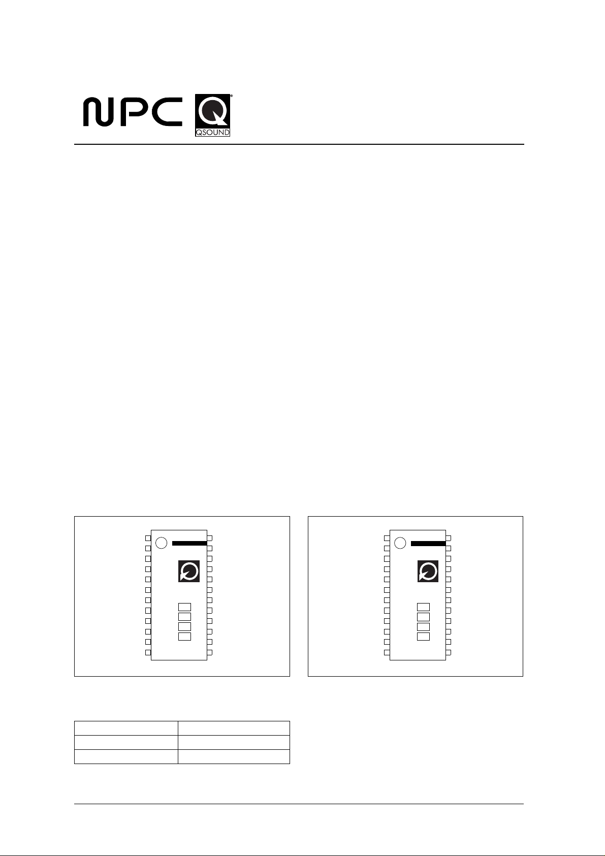
PINOUT
(Top view)
QS7779PM QS7779CM
■
Computer-based multimedia products, including
sound cards and powered loudspeakers
2
C 2 control pins serial inter-
QXAC3
QXAC2
QXAC1
RIN
LIN
COUT
CIN
VREFIN
VREFOUT
VREF
GND
SPRD(SCL)
1
QS7779PM
12
24
QXAC4
VCC
QXBC1
QXBC2
QXBC3
QXBC4
ROUT
LOUT
MUTE(STRB)
VDD
P/S
BYP(SDA)
13
Using these products does not require any Dolby certifications.
QXAC3
QXAC2
QXAC1
RIN
LIN
COUT
CIN
VREFIN
VREFOUT
VREF
GND
SPRD(SCL)
ORDERING INFORMATION
De vice Pack ag e
QS7779PM 24-pin SSOP
QS7779CM 24-pin SSOP
2
I
C bus is a registered trademark of Philips Electronics N.V.
Dolby and the double-D symbol are registered trademarks of Dolby Laboratories Licensing Corporation.
1
QS7779CM
12
NIPPON PRECISION CIRCUITS—1
24
13
QXAC4
VCC
QXBC1
QXBC2
QXBC3
QXBC4
ROUT
LOUT
MUTE
VDD
P/S
BYP(SDA)

PACKAGE DIMENSIONS
(Unit: mm)
10.05 0.20
10.20 0.30
QS7779PM/CM
7.80 0.30
5.40 0.20
0.15
0.10
+
−
0.05
0.8
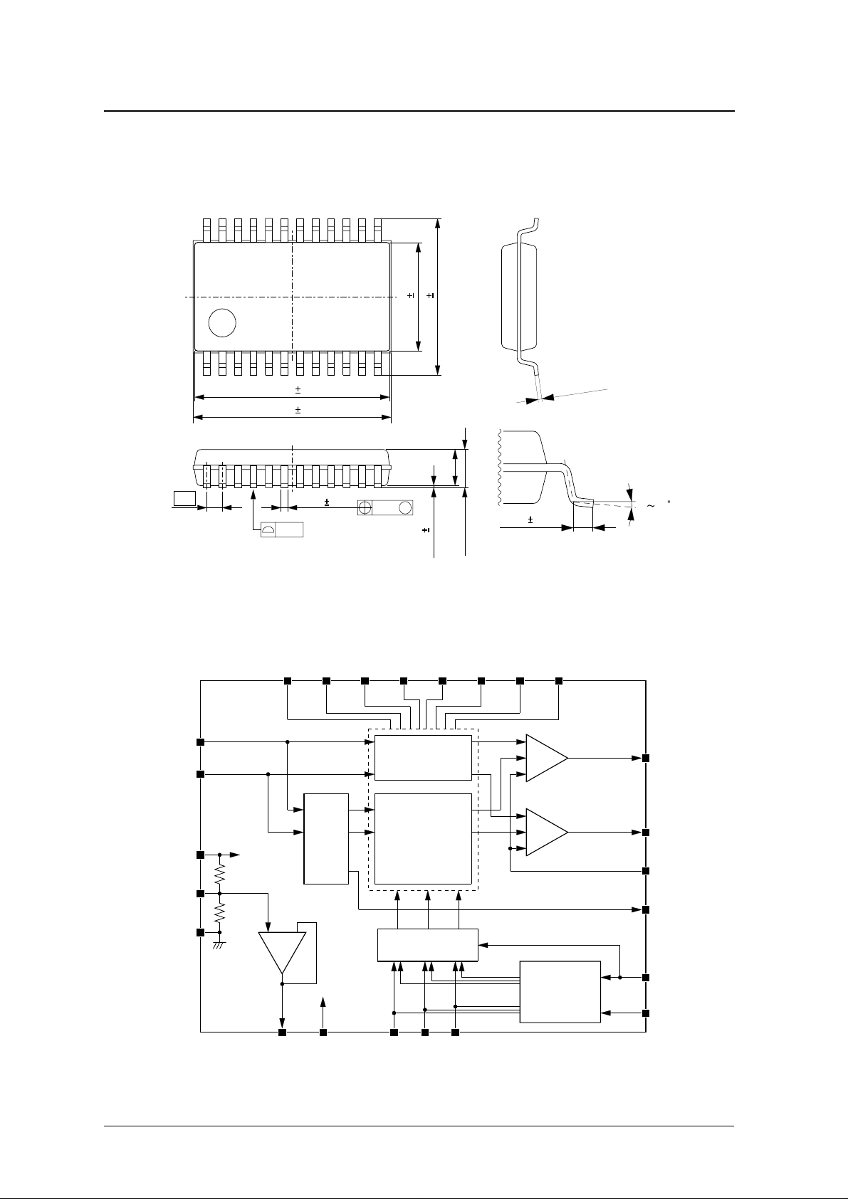
BLOCK DIAGRAM
RIN
4
LIN
5
23
VCC
GND
8
11
VREFIN
1.80
0.36 0.10
0.10
QXAC1QXAC2QXAC3QXAC4QXBC1 QXBC2QXBC3 QXBC4
123 2422212019
Surround
Decoder
910 121316
VREFOUT VREF
M
0.12
0.10 0.10
QXpander
Q1
Virtualization
Multiplex/Level Shift
BYP
(SDA)
MUTE
(STRB)
SPRD
(SCL)
+0.20
−0.10
1.90
0.50 0.20
Σ
Σ
Serial I/O
010
18
ROUT
17
LOUT
7
CIN
6
COUT
14
P/S
15
VDD
NIPPON PRECISION CIRCUITS—2

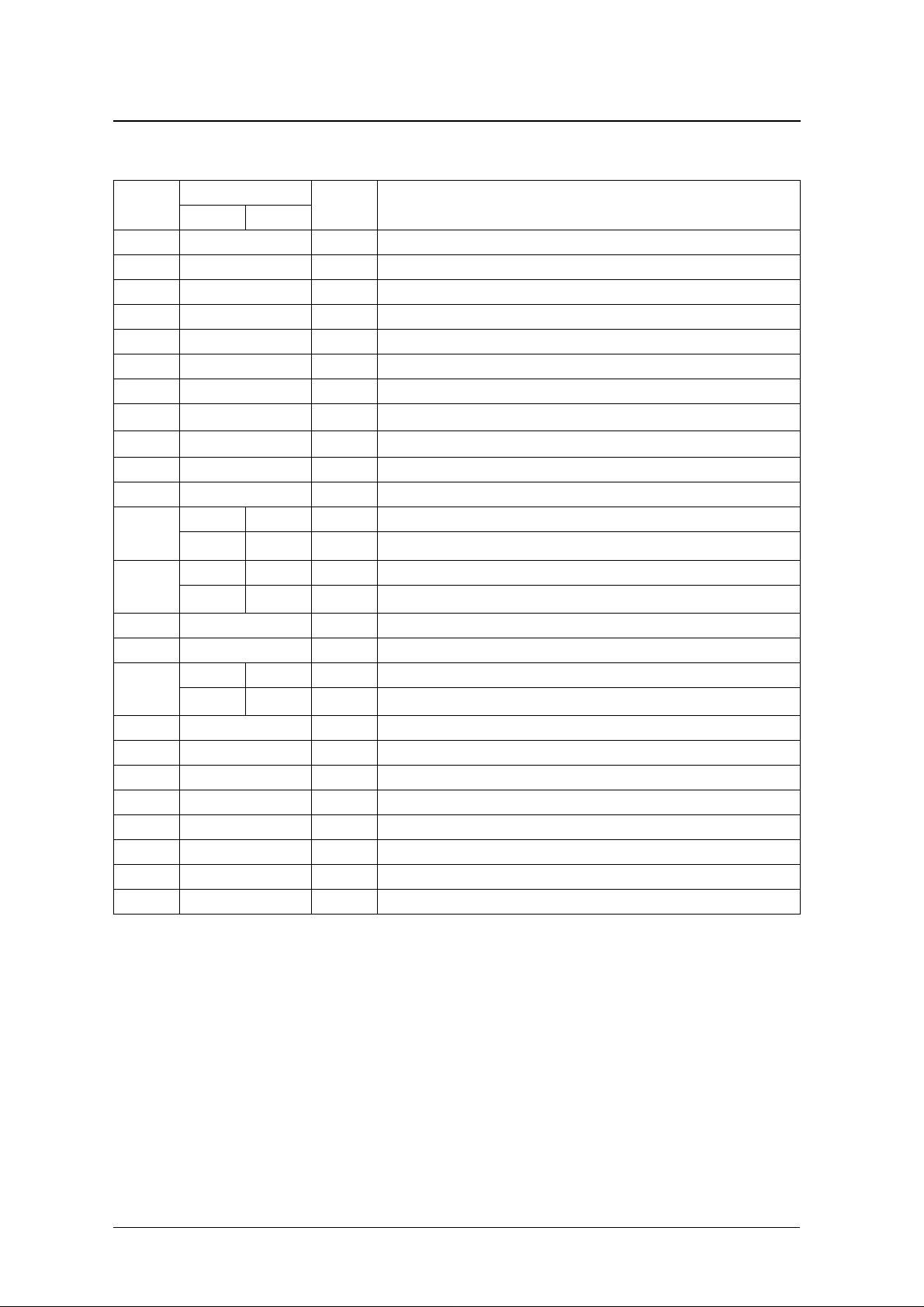
PIN DESCRIPTION
QS7779PM/CM
Number
I/O Description
Parallel Serial
1 Q X A C 3 I Capacitor 3 for QEXPANDER filter A
2 Q X A C 2 I Capacitor 2 for QEXPANDER filter A
3 Q X A C 1 I Capacitor 1 for QEXPANDER filter A
4 RI N I Right channel signal input
5 LIN I Left channel signal input
6 COUT O Decoded center signal output
7 CI N I Center signal input for summing with the right and the left signal outputs
Name
8 VREFIN O
9 VREFOUT O
Internally generated reference voltage (V
Buffered reference voltage (V
CC
/2)
CC
/2)
10 VREF I Signal reference input
11 GN D – Ground 0V
SPRD – I Enhancement control (H: spread maximum, L: spread minimum )
12
–
SCL
1
I Se r ial data shift clock
B Y P – I Bypass control (H: Bypass on, L: Qsurround on)
13
–
SDA
2
I/O
Se r ial data input. ACK data output for I
2
C (QS7779CM)
14 P/S I Interface mode control (H: parallel I/O, L: serial I/O)
15 V DD – Digital pow e r supply DC4.5 to 5.5V
MUTE – I Output mute control (H: m ute on, L: m ute off)
16
– STRB I
Ser ial data strobe (not applicable to I
2
C of QS7779CM)
17 LOUT O Left signal output
18 R OUT O Right signal output
19 QXBC4 I Capacitor 4 fo r QEXPANDER filter B
20 QXBC3 I Capacitor 3 fo r QEXPANDER filter B
21 QXBC2 I Capacitor 2 fo r QEXPANDER filter B
22 QXBC1 I Capacitor 1 fo r QEXPANDER filter B
23 VC C – Analog power supply DC5 to 13V
24 QXA C 4 I Capacitor 4 for QEXPANDER filter A
1. QS7779CM:CMOS input. No protective diode between the terminal and V D D.
QS7779PM:CMOS input. Protective diode is in between the terminal and V D D.
2. QS7779CM:Nch open drain terminal. No protective diode between terminal and V D D.
QS7779PM:CMOS input. Protective diode is in between the terminal and V D D.
NIPPON PRECISION CIRCUITS—3

SPECIFICATIONS
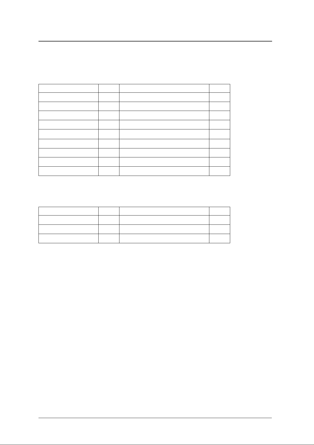
Absolute Maximum Ratings
GND = 0V
Parameter Symbol Rating Unit
Supply voltage (analog)
Supply voltage (digital)
Input voltage (analog)
Input voltage (digital)
2
I
C input voltage (SDA, SCL)
Po w er dissipation
Storage temperature
Soldering temperature
Soldering time
V
V
V
IANA
V
IDIG
V
IOPEN
P
T
T
SLD
t
SLD
CC
DD
D
stg
°
°
°
QS7779PM/CM
– 0.3 to 15 V
– 0.3 to 7 V
– 0.3 to V
– 0.3 to V
+ 0.3
CC
+ 0.3
DD
10 V
250 m W
– 40 to 125
255
10 sec
V
V
C
C
Recommended Operating Conditions
GND = 0V
Parameter Symbol Limits Unit
Supply voltage (analog)
Supply voltage (digital)
Operating temperature
V
V
T
CC
DD
OPR
5 to 13
4.5 to 5.5 V
– 20 to 70
V
C
NIPPON PRECISION CIRCUITS—4
 Loading...