NPC NR8576AA, NR8576BA, NR8576AB, NR8576BB Datasheet

NR8576 Series
NIPPON PRECISION CIRCUITS INC.
OVERVIEW
The NR8576 Series devices are serial-interface type
real-time clock module ICs with built-in crystal
oscillator elements. They feature timer counter circuits that keep track of time from the current second
to the current year, automatic leap-year adjustment,
and a supply voltage detect function. Also, a 32.768
kHz/1 Hz select output function is incorporated for
independent hardware control. They are available in
compact 14-pin SOPs (NR8576A × ) and miniature
18-pin SOPs (NR8576B × ).
FEATURES
Crystal oscillator element built-in for adjustment-
■
free use
■
Timer counters for second, minute, hour, day, day
of the week, month, and year
■
2.5 to 5.5 V operating voltage range
■
1.7 ± 0.3 V supply voltage detection threshold
■
1.0 µA at 3.0 V (typ) current consumption
■
Automatic leap-year calendar adjustment
■
32.768 kHz and 1 Hz output selectable
■
Package
• 14-pin SOP (NR8576A × )
• 18-pin SOP (NR8576B × )
SERIES CONFIGURATION
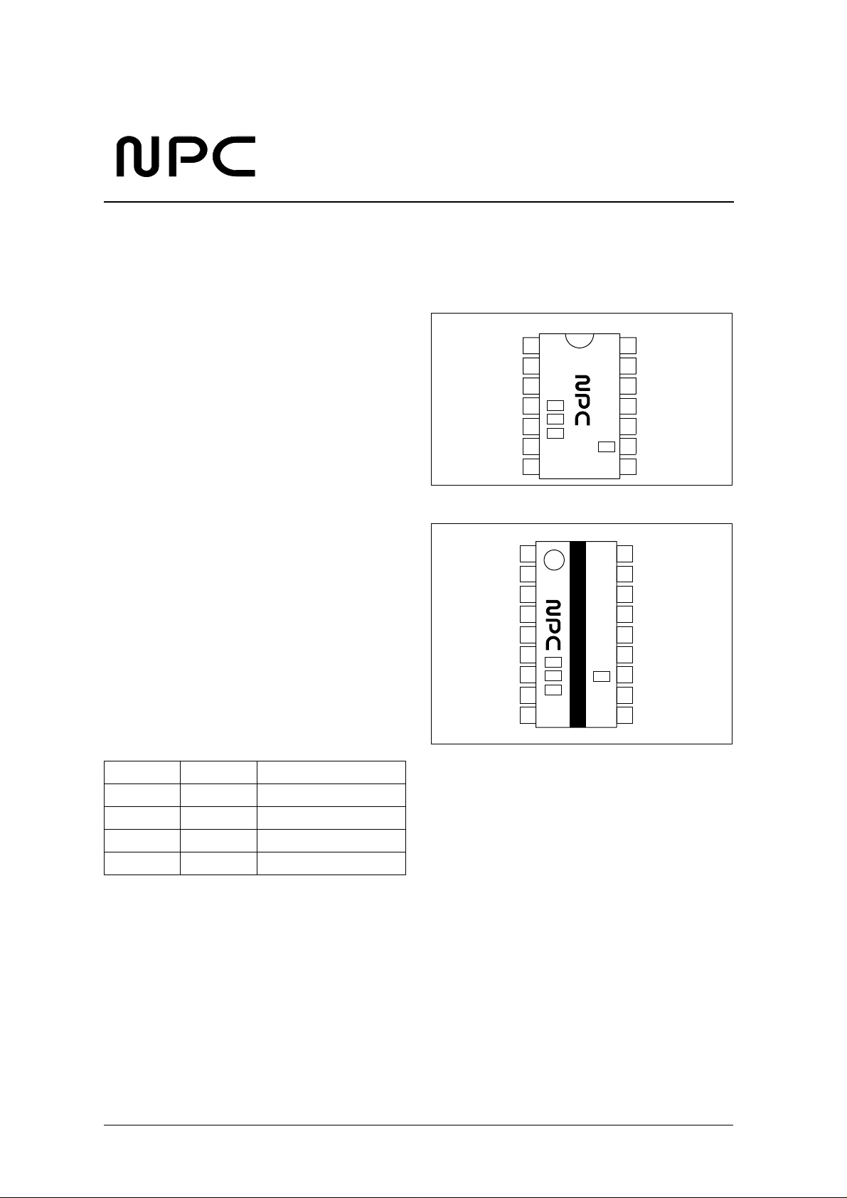
PINOUTS
14-pin SOP
18-pin SOP
FSEL
Real-time Clock Modules
1
VSS
2
N.C
3
CE
4
FSEL
5
WR
6
FOE
7
N.C N.C
1
N.C
2
N.C
3
N.C
4
N.C
5
FOE
6
WR
7
811
CE
VSS
14
NR8576A
NR8576B
FOUT
13
N.C
12
N.C
11
DATA
10
CLK
9
VDD
8
18
N.C
17
N.C
16
N.C
15
N.C
VDD
14
N.C
13
12
CLK
DATA
109
FOUT
Device Package Frequency deviation
NR8576AA 14-pin SOP 5 ± 12 ppm
NR8576AB 14-pin SOP 5 ± 23 ppm
NR8576BA 18-pin SOP 5 ± 12 ppm
NR8576BB 18-pin SOP 5 ± 23 ppm
NIPPON PRECISION CIRCUITS—1

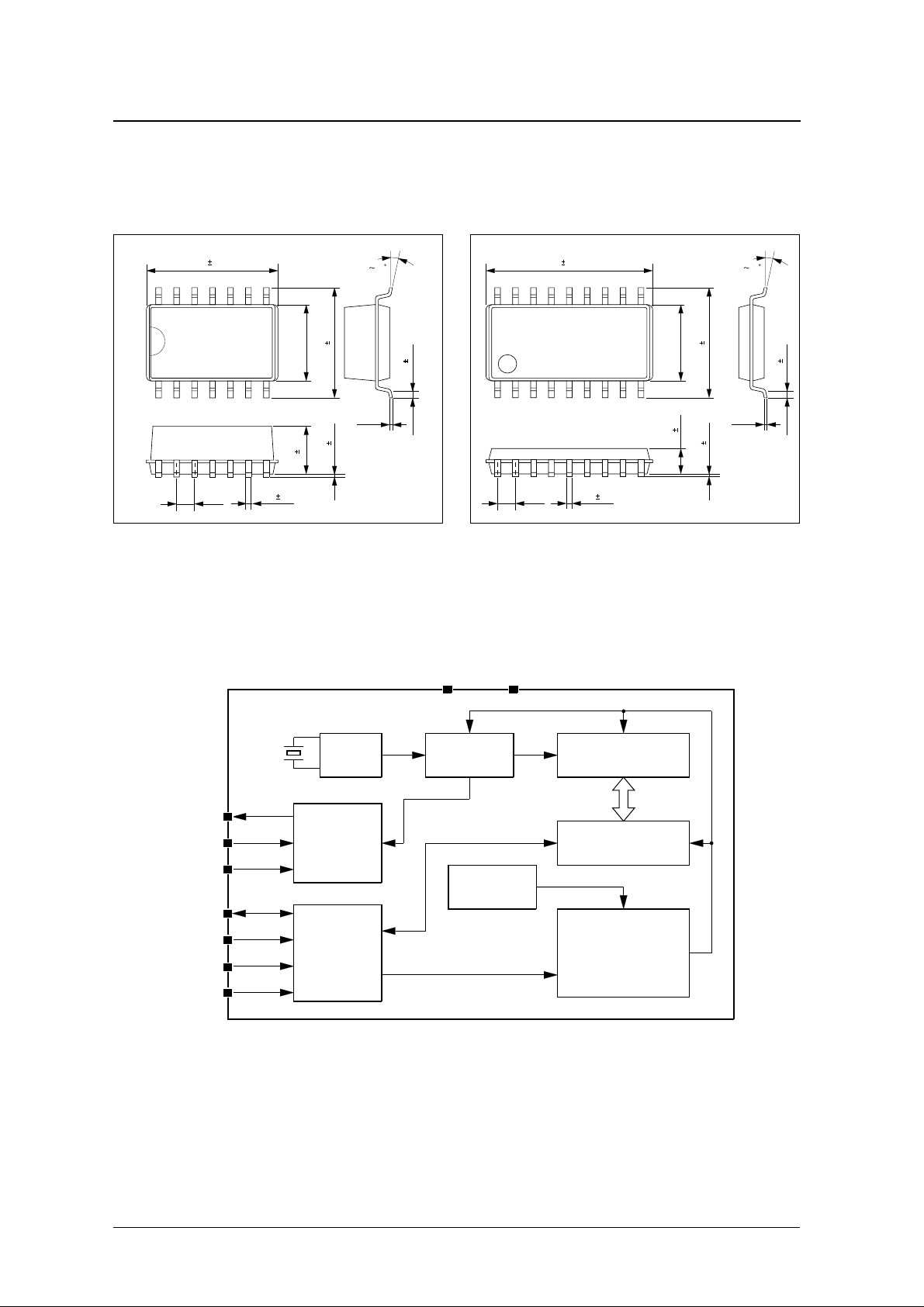
PACKAGE DIMENSIONS
Unit: mm
NR8576 Series
14-pin SOP
10.1 0.2
1.27
0.35 0.1
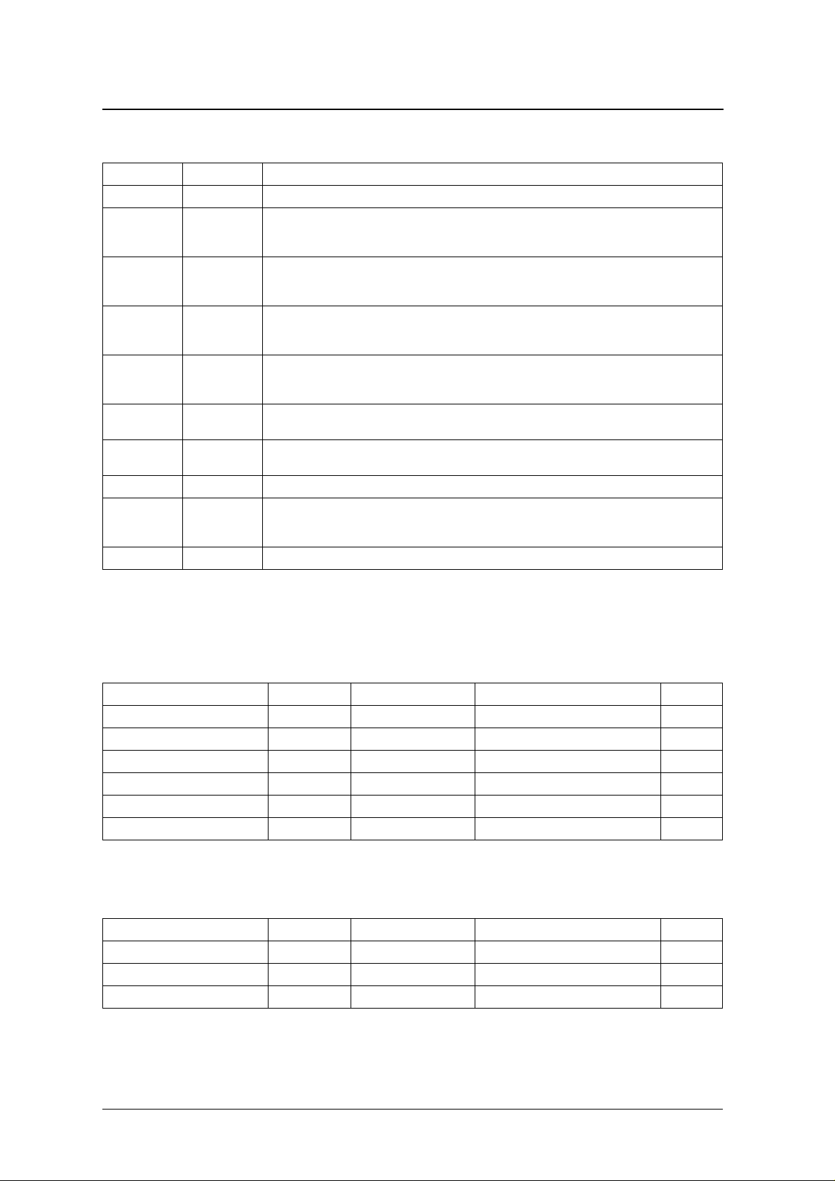
BLOCK DIAGRAM
5.0
3.2 0.1
7.4 0.2
0.10 0.05
010
0.15
0.6 0.2
18-pin SOP
1.27
11.4 0.2
0.4 0.1
5.4
1.8 0.1
010
7.8 0.2
0.6 0.2
0.15
0.05 0.05
FOUT
FSEL
FOE
DATA
CLK
WR
CE
32.768kHz
OSC
Output
Controller
I/O
Controller
VDD VSS
Divider Timer Counter
Shift Register
Voltage
Detect
Control
Circuit
NIPPON PRECISION CIRCUITS—2

−
−
−
−
°
°
−
°
NR8576 Series
PIN DESCRIPTION
Name I/O Description
VSS – Ground
CE I
FSEL I
WR I
FOE I
VDD –
CLK I
DATA I/O Data read and write input/output
FOUT O
N. C – No connection. Leave open for normal use.
Chip enable.
HIGH: Enable
LOW: DATA goes high impedance; input on WR, CLK, and DATA stops; and the TM bit is cleared.
FOUT output frequency select.
HIGH: 1 Hz
LOW: 32.768 kHz
DATA input/output control switch.
HIGH: Data input mode (RTC write)
LOW: Data output mode (RTC read)
FOUT output enable control.
HIGH: The frequency selected by FSEL is output on FOUT.
LOW: FOUT goes high impedance.
Supply voltage.
Connect a ≥ 0.1 µF capacitor between VDD and VSS.
System clock input.
Data is input (RTC write mode) and output (RTC read mode) on the rising edge of CLK.
Frequency output (output controlled by FOE and frequency selected by FSEL).
In 1 Hz output mode, the 1 Hz signal is synchronized to the internal 1 second signal.
FOUT output is not affected by the CE signal.
SPECIFICATIONS
Absolute Maximum Ratings
V
= 0 V
SS
Parameter Symbol Condition Rating Unit
Supply voltage range V
Input voltage range V
Output voltage range V
Storage temperature range T
Soldering temperature T
Soldering time t
DD
IN
OUT
stg
sld
sld
Recommended Operating Conditions
V
= 0 V
SS
Parameter Symbol Condition Rating Unit
Supply voltage range V
Clock supply voltage range V
Operating temperature range T
DD
CLK
opr
T
a
T
a
T
a
= 25 ° C
= 25 ° CV
= 25 ° CV
0.3 to 7.0 V
SS
SS
0.3 to V
0.3 to V
+ 0.3 V
DD
+ 0.3 V
DD
55 to 125
260
10 s
2.5 to 5.5 V
1.4 to 5.5 V
40 to 85
C
C
C
NIPPON PRECISION CIRCUITS—3
 Loading...